

Page 1
19-0388; Rev 1; 3/96
EVALUATION KIT MANUAL
FOLLOWS DATA SHEET
Low-Noise, Regulated, -2V GaAsFET Bias
_______________General Description
The MAX840/MAX843/MAX844 low-noise, inverting
charge-pump power supplies are ideal for biasing
GaAsFETs in cellular telephone transmitter amplifiers.
They operate with inputs down to 2.5V.
The MAX840 offers both a -2V preset output and a -0.5V
to -9.4V adjustable output. The MAX843/MAX844 use
an external positive control voltage to set the negative
output voltage. Input voltage range for all the devices is
2.5V to 10V, and output current is 4mA with VIN> 2.7V.
These circuits can operate with small capacitors, as low
as 0.22µF.
An internal linear regulator reduces the MAX840’s output voltage ripple to 1mVp-p. With a well-filtered control
voltage (V
), the MAX843/MAX844 also achieve less
CTRL
than 1mVp-p typical output ripple. Supply current is
750µA, and reduces to less than 1µA in shutdown
(MAX840/MAX843). The MAX844’s unregulated output
is active in shutdown, with the charge pump switching at
20kHz. It provides a low-power LCD supply.
________________________Applications
Cellular Phones
GaAsFET Power Amplifier Modules
Personal Communicators, PDAs
Wireless Data Loggers
Continuously Adjustable GaAsFET Bias
LCD-Bias Contrast Control
Regulated Negative Power Supplies
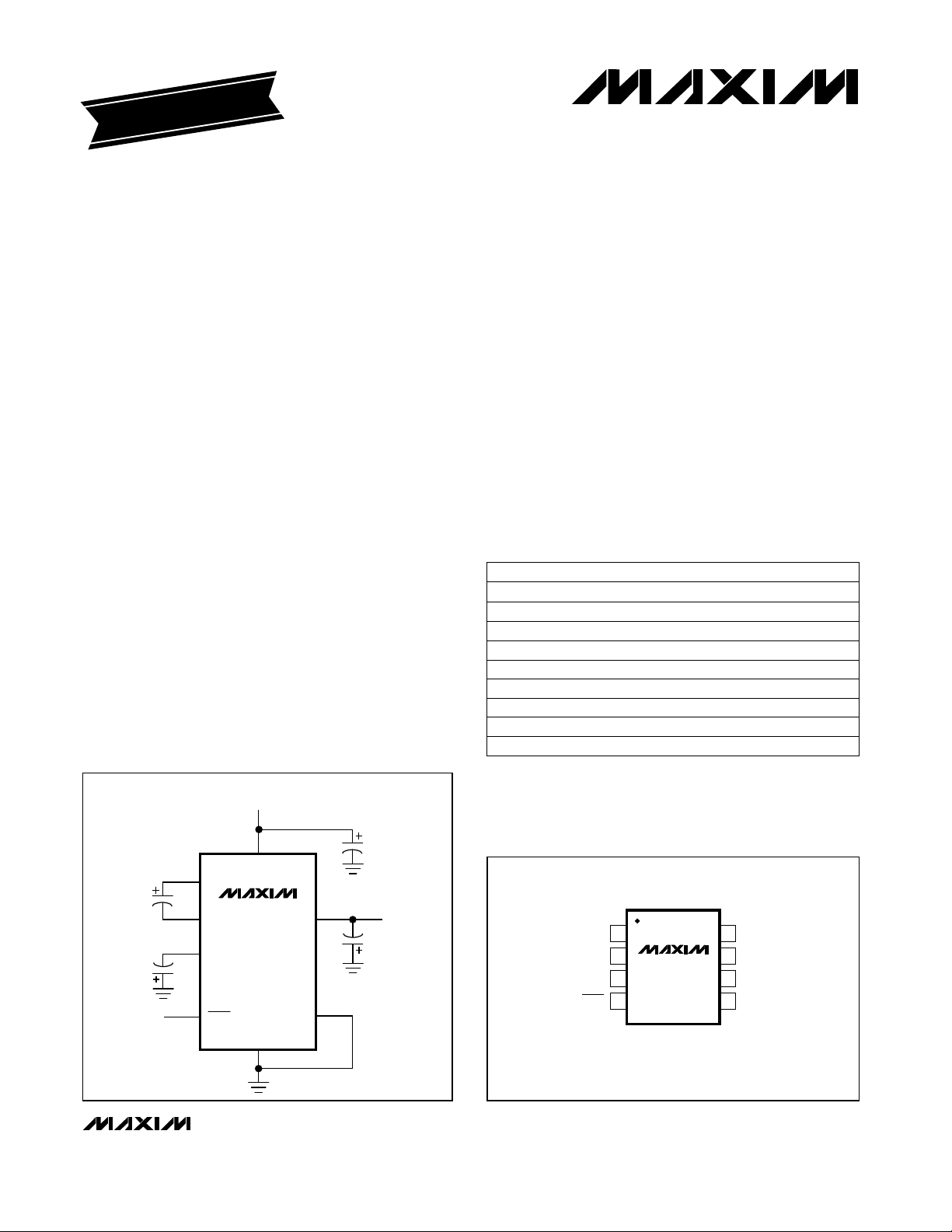
__________Typical Operating Circuit
VIN = 2.5V to 10.0V
(3 CELLS)
____________________________Features
♦ Fixed -2V or Adjustable -0.5V to -9.4V Output
at 4mA (MAX840)
♦ 2.5V to 10V Input Voltage Range
♦ Operate with Small Capacitors (as low as 0.22µF)
♦ 1mVp-p Output Voltage Ripple
♦ Charge-Pump Switching Frequency:
100kHz in Normal Operation
20kHz in Shutdown Mode (MAX844)
♦ 1µA Max Logic-Level Shutdown Over Temp.
(MAX840/MAX843)
♦ Small 8-Pin SO Package
______________Ordering Information
PART
MAX840C/D
MAX840ISA
MAX840ESA -40°C to +85°C
MAX843C/D
MAX843ISA -25°C to +85°C 8 SO
MAX843ESA -40°C to +85°C 8 SO
MAX844C/D
MAX844ISA -25°C to +85°C 8 SO
MAX844ESA -40°C to +85°C 8 SO
* Dice are specified at TA= +25°C only.
TEMP. RANGE PIN-PACKAGE
0°C to +70°C
-25°C to +85°C
0°C to +70°C Dice*
0°C to +70°C Dice*
Dice*
8 SO
8 SO
MAX840/MAX843/MAX844
__________________Pin Configuration
TOP VIEW
1
C1+
2
C1-
NEGOUT
3
SHDN
4
( ) ARE FOR MAX843/MAX844
MAX840
MAX843
MAX844
SO
Maxim Integrated Products
8
7
6
5
IN
GND
OUT
FB (CONT)
1
0.22µF
0.22µF
ON/OFF
0.22µF
C1+
C1-
NEGOUT
SHDN
________________________________________________________________
IN
MAX840
GND
OUT
= -2.0V
V
OUT
of GaAsFET)
(V
GG
4.7µF
FB
For free samples & the latest literature: http://www.maxim-ic.com, or phone 1-800-998-8800
Page 2
Low-Noise, Regulated, -2V GaAsFET Bias
ABSOLUTE MAXIMUM RATINGS
Supply Voltage, V
V
NEGOUT
V
IN
V
OUT
V
SHDN
to GND...................................................-10.5V to 0.3V
to V
NEGOUT
to GND (Note 1).......................................V
to GND ............................................-0.3V to (VIN+ 0.3V)
Continuous Power Dissipation (T
to GND ..................................-0.3V to 10.5V
IN
.........................................................-0.3V to 21V
to 0.3V
= +70°C)
A
NEGOUT
SO (derate 5.88mW/°C above +70°C).........................471mW
Note 1: The output may be shorted to NEGOUT or GND if the package power dissipation is not exceeded. Typical short-circuit
current from 4V to GND is 40mA.
Stresses beyond those listed under “Absolute Maximum Ratings” may cause permanent damage to the device. These are stress ratings only, and functional
operation of the device at these or any other conditions beyond those indicated in the operational sections of the specifications is not implied. Exposure to
absolute maximum rating conditions for extended periods may affect device reliability.
ELECTRICAL CHARACTERISTICS
(Figures 2a and 2c, 2.5V ≤ VIN≤ 10V, V
Typical values are measured at VIN= 3.6V and TA= +25°C.)
Supply Voltage Range
Output Voltage
MAX840/MAX843/MAX844
Output Voltage Adjust Range
V
V
FB Voltage
FB Leakage Current
CONT Leakage Current
CONT
Supply Current µA750 1300
Shutdown Supply Current
V
Load Regulation
OUT
Ripple
OUT
I
SHUT
Oscillator Frequency F
Input High Voltage V
Input Low Voltage V
Input Current I
Input Capacitance C
= -2V, GND = 0V, RL= ∞, SHDN = VIN, TA= T
OUT
IN
MAX840, VFB= 0V
OUT
MAX843/MAX844,
V
= 2V
CTRL
OUT
MAX840, no load
FB
FB
MAX840, VFB= -0.5V
MAX843/MAX844, V
No load, VIN≤ 3.6VI
Q
MAX840/MAX843, VIN= 10V, SHDN = 0V
MAX844, VIN= 10V, SHDN = 0V
MAX844, VIN≤ 3.6V, SHDN = 0V
VIN= 3.6V,
RL= ∞ or 500Ω
C4 = 10µF
OSC
VIN= 3.6V,
TA= +25°C
SHDN 2.2 V
IH
SHDN 0.35 V
IL
SHDN -1 1 µA
IN
SHDN 10 pF
IN
Operating Temperature Ranges
MAX84_I_ _A ...................................................-25°C to +85°C
MAX84_E_ _A ..................................................-40°C to +85°C
Storage Temperature Range.............................-65°C to +150°C
Lead Temperature (soldering, 10sec).............................+300°C
to T
MIN
, unless otherwise noted.
MAX
CONDITIONS
VIN≥ 2.5V,
I
= 0mA to 3mA
OUT
VIN≥ 2.7V,
I
= 0mA to 4mA
OUT
VIN≥ 2.5V,
I
= 0mA to 3mA
OUT
VIN≥ 2.7V,
I
= 0mA to 4mA
OUT
-2.1 -2.0 -1.9
-2.1 -2.0 -1.9
-2.05 -2.0 -1.95
-2.05 -2.0 -1.95
-0.5 to
- 0.6)
(V
IN
= 0V
CONT
1
940
175 300
MAX840, VFB= 0V
MAX843/MAX844,
V
= 2V
CTRL
MAX840/MAX843/
MAX844
MAX844, SHDN = 0V
80 100 120
14 20 26
38
28
UNITSMIN TYP MAXSYMBOLPARAMETER
mV/mA
mVp-p1V
V2.5 10V
V
V
V-0.516 -0.5 -0.484V
nA±1 ±100I
nA±1 ±100I
µA
kHz
2 _______________________________________________________________________________________
Page 3
Low-Noise, Regulated, -2V GaAsFET Bias
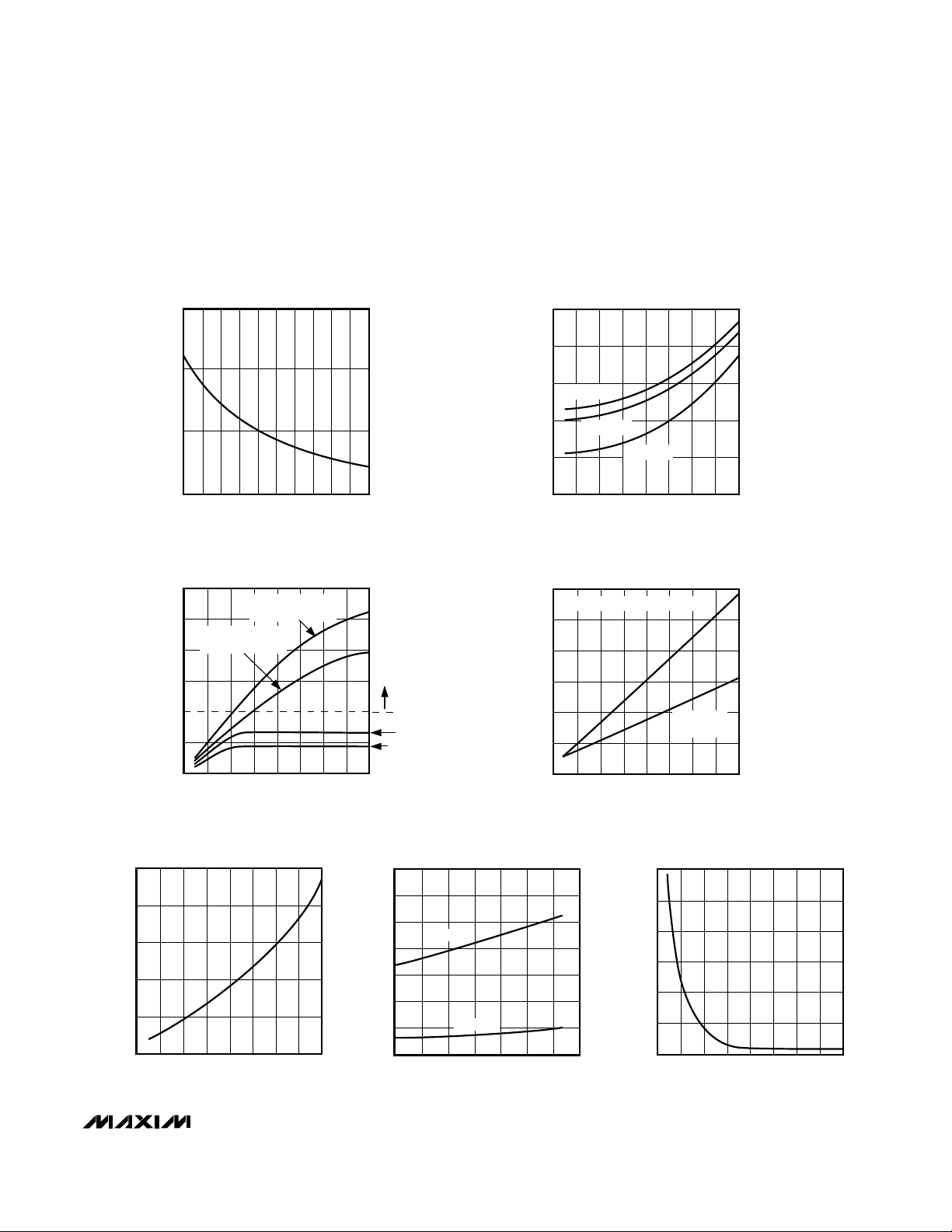
__________________________________________Typical Operating Characteristics
(Circuit of Figure 2a, VIN= 3.6V, TA= +25°C, unless otherwise noted.)
OUTPUT VOLTAGE
vs. OUTPUT CURRENT
-2.070
MAX840-01
-2.060
-2.050
OUTPUT VOLTAGE (V)
-2.040
010
24 8
13579
OUTPUT CURRENT (mA)
6
MAXIMUM OUTPUT CURRENT
vs. INPUT VOLTAGE
120
100
80
60
V
(CIRCUIT OF FIG 2d)
(CIRCUIT OF FIG 2a)
< -1.95V
OUT
V
< -1.95V
OUT
MAX840-03
High-current operation not
recommended for extended
periods of time.
OUTPUT VOLTAGE vs. INPUT VOLTAGE
OVER TEMPERATURE
-2.065
-2.060
-2.055
T
= +85°C
A
-2.050
OUTPUT VOLTAGE (V)
-2.045
-2.040
TA = +25°C
TA = -40°C
INPUT VOLTAGE (V)
NEGOUT CURRENT vs. INPUT VOLTAGE
30
V
= 0.9 x V
NEGOUT
25
20
15
NEGOUT(NO LOAD)
MAX840-02
10624 83579
MAX840-04
MAX840/MAX843/MAX844
40
20
MAXIMUM OUTPUT CURRENT (mA)
0
24 83579
INPUT VOLTAGE (V)
N0-LOAD SUPPLY CURRENT
vs. INPUT VOLTAGE
5
4
3
2
1
NO-LOAD SUPPLY CURRENT (mA)
0
24 83579
6
INPUT VOLTAGE (V)
_______________________________________________________________________________________
V
< 2mVp-p RIPPLE
OUT
(CIRCUIT OF FIG 2a)
V
< 2mVp-p RIPPLE
OUT
(CIRCUIT OF FIG 2d)
6
10
10
NEGOUT CURRENT (mA)
5
0
24 83579
INPUT VOLTAGE (V)
SUPPLY CURRENT vs. TEMPERATURE
7
MAX840-05
SUPPLY CURRENT (mA)
10
6
5
4
3
2
1
0
VIN = 10V
VIN = 3.6V
-40 0 80-20 20 60 100
TEMPERATURE (°C)
40
MAX840-06
START-UP TIME (ms)
SHUTDOWN
(MAX844)
6
10
START-UP TIME vs. INPUT VOLTAGE
2.8
2.4
2.0
1.6
1.2
0.8
0.4
24 8357910
6
INPUT VOLTAGE (V)
MAX840-07
3
Page 4

Low-Noise, Regulated, -2V GaAsFET Bias
____________________________Typical Operating Characteristics (continued)
(Circuit of Figure 2a, VIN= 3.6V, TA= +25°C, unless otherwise noted.)
OSCILLATOR FREQUENCY
vs. SUPPLY VOLTAGE
150
140
130
120
110
100
90
OSCILLATOR FREQUENCY (kHz)
80
70
T
24 83579
SUPPLY VOLTAGE (V)
= +25°C, +85°C
A
6
MAX840-17
TA = -40°C
SHDN = HIGH
10
MAX840 OUTPUT NOISE AND RIPPLE
(C1 = C2 = C3 = 1µF, C4 = 10µF)
MAX840/MAX843/MAX844
V
OUT
500µV/div
OSCILLATOR FREQUENCY vs. SUPPLY VOLTAGE
MAX844
31
29
27
25
23
21
19
OSCILLATOR FREQUENCY (kHz)
17
15
24 83579
T
= +25°C, +85°C
A
TA = -40°C
SHDN = LOW
6
SUPPLY VOLTAGE (V)
MAX840 OUTPUT NOISE AND RIPPLE
(C1 = C2 = C3 = 0.22µF, C4 = 4.7µF)
MAX840-18
10
V
OUT
1mV/div
10µs/div
VIN = 3.6V, V
OUT
= -2V, I
= 4mA, AC COUPLED
OUT
MAX843/MAX844 OUTPUT NOISE AND RIPPLE
(C1 = C2 = C3 = 1µF, C4 = 10µF)
10µs/div
VIN = 3.6V, V
OUT
= -2V, I
= 4mA, AC COUPLED
OUT
V
OUT
500µV/div
VIN = 3.6V, V
OUT
MAX843/MAX844 OUTPUT NOISE AND RIPPLE
(C1 = C2 = C3 = 0.22µF, C4 = 4.7µF)
VIN = 3.6V, V
OUT
= -2V, I
= -2V, I
10µs/div
= 4mA, AC COUPLED
OUT
10µs/div
= 4mA, AC COUPLED
OUT
4 _______________________________________________________________________________________
V
OUT
1mV/div
Page 5

Low-Noise, Regulated, -2V GaAsFET Bias
____________________________Typical Operating Characteristics (continued)
(Circuit of Figure 2a, VIN= 3.6V, TA= +25°C, unless otherwise noted.)
MAX840 NOISE SPECTRUM
40
VIN = 3.6V,
I
OUT
30
20
10
NOISE (dBµV)
0
-10
0.1 1
50
VIN = 3.6V,
I
OUT
40
= 4mA
= 4mA
(C1 = C2 = C3 = 1µF, C4 = 10µF)
10 100 1000
FREQUENCY (kHz)
MAX840 NOISE SPECTRUM
(C1 = C2 = C3 = 0.22µF, C4 = 4.7µF)
MAX840/MAX843/MAX844
NOTE: dBµV = 20 LOG
V
OUT
______
1µV
30
20
NOISE (dBµV)
10
0
0.1 1
40
VIN = 3.6V,
I
OUT
30
20
10
NOISE (dBµV)
0
-10
0.1 1
10 100 1000
FREQUENCY (kHz)
MAX843/MAX844 NOISE SPECTRUM
(C1 = C2 = C3 = 1µF, C4 = 10µF)
= 4mA
10 100 1000
FREQUENCY (kHz)
_______________________________________________________________________________________
5
Page 6

Low-Noise, Regulated, -2V GaAsFET Bias
____________________________Typical Operating Characteristics (continued)
(Circuit of Figure 2a, VIN= 3.6V, TA= +25°C, unless otherwise noted.)
MAX843/MAX844 NOISE SPECTRUM
(C1 = C2 = C3 = 0.22µF, C4 = 4.7µF)
50
VIN = 3.6V,
= 4mA
I
OUT
40
30
20
NOISE (dBµV)
10
0
NOTE: dBµV = 20 LOG
V
OUT
______
1µV
0.1 1
FREQUENCY (kHz)
START-UP FROM SHUTDOWN
MAX840/MAX843/MAX844
0V
0V
500µs/div
VIN = 3.6V, V
LOAD-TRANSIENT RESPONSE
= -2V, I
OUT
V
OUT
20mV/div
OUT
10 100 1000
V
OUT
1V/div
V
SHDN
2V/div
= 4mA
LINE-TRANSIENT RESPONSE
V
OUT
10mV/div
0.01mA
I
OUT
4mA
5ms/div
= 4mA, AC COUPLED
VIN = 3.6V, V
OUT
= -2V
5ms/div
V
OUT
= -2V, I
OUT
6 _______________________________________________________________________________________
3.3V
2.7V
V
IN
Page 7

Low-Noise, Regulated, -2V GaAsFET Bias
______________________________________________________________Pin Description
PIN
MAX840
1 C1+ Positive Terminal for C1
2 C1- Negative Terminal for C1
3 NEGOUT Negative Output Voltage (unregulated)
4 SHDN Active-Low, TTL Logic-Level Shutdown Input
5 FB
— CONT
6 OUT Regulated Negative Output Voltage
7 GND Ground
8 IN Positive Power-Supply Input
Dual Mode is a trademark of Maxim Integrated Products.
MAX843
MAX844
1
2
3
4
—
5
6
7
8
NAME FUNCTION
Dual Mode™ Feedback Input. When FB is grounded, the output is preset to -2V. To
select other output voltages, connect FB to an external resistor divider (Figure 2b).
Control Voltage Input. To set V
, connect a resistor divider between OUT and a
OUT
positive control voltage between 0V and 10V (Figure 2c).
MAX840/MAX843/MAX844
C1+
CHARGE
-0.5V
REF
PUMP
N
C1-
NEGOUT
SHDN
Figure 1a. MAX840 Block Diagram
_______________________________________________________________________________________ 7
MAX840
GND
IN
OUT
FB
CONNECT TO
GND TO SET
V
= -2V
OUT
C1+
CHARGE
C1-
PUMP
MAX843
MAX844
GND
SHDN
NEGOUT
N
Figure 1b. MAX843/MAX844 Block Diagram
IN
OUT
CONT
CONTROL
VOLTAGE
R2
R1
Page 8

Low-Noise, Regulated, -2V GaAsFET Bias
_______________Detailed Description
The MAX840/MAX843/MAX844 are low-noise, inverting,
regulated charge-pump power supplies designed for
biasing GaAsFET devices, such as power-amplifier
modules in cellular handsets.
The applied input voltage (VIN) is first inverted to a negative voltage at NEGOUT by a capacitive charge pump.
This voltage is then regulated by an internal low-noise
linear regulator, and appears at OUT (Figure 1). The
minimum (most negative) output voltage achievable is
the inverted positive voltage, plus the 0.6V required by
the post-regulator. For the MAX840, the linear regulator
reduces ripple noise induced by the charge-pump
inverter to 1mVp-p at V
lator’s excellent AC rejection attenuates noise from the
incoming supply.
. In addition, the linear regu-
OUT
__________Applications Information
Setting the Output Voltage
For the MAX840, select either a fixed or adjustable
output voltage. Connect FB directly to GND for a fixed
-2V output (Figure 2a). Select an alternate output voltage by connecting FB to the midpoint of a resistor
voltage divider from OUT to GND (Figure 2b). V
MAX840/MAX843/MAX844
must be 0.6V above the absolute value of V
allow proper regulation. The output voltage is calculated from the formula below. Choose R2 to be between
100kΩ and 400kΩ.
V
= (-0.5V)(1 + R2 / R1)
OUT
For the MAX843/MAX844, set the output voltage by
connecting a resistor voltage divider between OUT and
a positive control voltage (V
V
= -V
OUT
CTRL
) (Figure 2c).
CTRL
(R2 / R1)
Shutdown Mode
The MAX840/MAX843/MAX844 feature a shutdown
mode that reduces the supply current to 1µA max over
temperature (300µA max for the MAX844). When the
MAX840/MAX843 are in shutdown, the outputs (OUT,
NEGOUT) and the charge-pump oscillator are disabled. When the MAX844 is in shutdown, only the linear regulator is disabled and the NEGOUT output
remains enabled. However, the charge-pump oscillation frequency is reduced to 20kHz, reducing the
available power at NEGOUT. The output voltage at
NEGOUT can be used to bias an LCD while in shutdown.
OUT
IN
to
Capacitors
Use capacitors with low effective series resistance
(ESR) to maintain a low dropout voltage (VIN- |V
The overall dropout voltage is a function of the charge
pump’s output resistance and the voltage drop across
the linear regulator (N-channel pass transistor). At the
100kHz switching frequency, the charge-pump output
resistance is a function of C1 and C2’s ESR. Therefore,
minimizing the ESR of the charge-pump capacitors
minimizes the dropout voltage.
The output resistance of the entire circuit is approximately:
R
= RO+ 4 x ESRC1+ ESRC4+
OUT
1 / (fSx C1) + R
where [RO+ R
of the internal switches and the resistance across the
linear regulator, is approximately 71Ω at VIN= 2.5V,
48Ω at VIN= 5V, and 40Ω at VIN= 10V.
C1, C2, and C3 should be 1µF capacitors with less than
0.8Ω ESR. C4 should be a 10µF capacitor with less
than 0.2Ω ESR. Smaller capacitor values can be used
(C1 = C2 = C3 = 0.22µF, C4 = 4.7µF) with a small
increase in output noise and ripple (Figure 2d). All
capacitors should be either surface-mount chip tantalum or ceramic types. External capacitor values can be
adjusted to optimize size and cost.
(linear regulator)
(linear regulator)
], the effective resistance
OUT
|
Layout and Grounding
Good layout is important, primarily for good noise performance. Take the following steps to ensure good layout:
1) Mount all components as close together as possible.
2) Keep traces short to minimize parasitic inductance
and capacitance. This includes connections to FB.
3) Use a ground plane.
Noise and Ripple Measurement
Accurately measuring the output noise and ripple is a
challenge. Slight momentary differences in ground
potential between the MAX840/MAX843/MAX844 circuit
and the oscilloscope (which results from the charge
pump’s switching action) cause ground currents in the
probe’s wires, inducing sharp voltage spikes. For best
results, measure directly across the output capacitor
(C4). Do not use the ground lead of the oscilloscope
probe; instead, remove the probe’s tip cover and touch
the ground ring on the probe directly to C4’s ground
terminal. You can also use a Tektronix chassis-mount
test jack (part no. 131-0258) to connect your scope
probe directly. This direct connection gives the most
accurate noise and ripple measurement.
).
8 _______________________________________________________________________________________
Page 9

Low-Noise, Regulated, -2V GaAsFET Bias
MAX840/MAX843/MAX844
C1
1µF
C2
1µF
ON/OFF
V
IN
8
1
C1+
2
C1-
3
NEGOUT
45
SHDN
IN
MAX840
GND
OUT
FB
C3
1µF
= -2V
V
OUT
of GaAsFET)
(V
6
GG
C4
10µF
7
C1
1µF
C2
1µF
ON/OFF
1
2
3
4
C1+
C1-
NEGOUT
SHDN
V
IN
IN
MAX840
GND
8
V
= (-0.5V) 1+
OUT
6
OUT
R2
100k
5
FB
R1
7
100k
Figure 2a. MAX840 Standard Application Circuit Figure 2b. MAX840 Adjustable Configuration
C1
1µF
C2
1µF
ON/OFF
V
IN
8
1
C1+
2
C1-
3
NEGOUT
45
SHDN
IN
V
OUT
MAX843
MAX844
OUT
6
CONT
GND
7
V
(0V TO 10V)
CTRL
= -0.5V to -9.4V @ 4mA
R2
100k
R1
100k
C3
1µF
C4
10µF
0.22µF
0.22µF
ON/OFF
1
C1
2
3
C2
45
C1+
C1-
NEGOUT
SHDN
V
IN
8
IN
MAX840
GND
7
6
OUT
FB
C3
0.22µF
V
OUT
of GaAsFET)
(V
GG
C4
4.7µF
C3
1µF
R2
( )
R1
C4
10µF
= -2V
Figure 2c. MAX843/MAX844 Standard Application Circuit
_______________________________________________________________________________________ 9
Figure 2d. MAX840 Application Circuit Using Smaller Capacitors
Page 10

Low-Noise, Regulated, -2V GaAsFET Bias
___________________Chip Topography
IN
C1+
GND
GND
NEGOUT
NEGOUT
C1-
0.145"
(3.683mm)
MAX840/MAX843/MAX844
SHDN
0.085"
(2.159mm)
FB (CONT)
OUT
( ) ARE FOR MAX843/MAX844
TRANSISTOR COUNT: 148
SUBSTRATE CONNECTED TO IN
10 ______________________________________________________________________________________
 Loading...