

Page 1
19-0167; Rev 2; 6/95
EVALUATION KIT MANUAL
FOLLOWS DATA SHEET
5V/3.3V/3V/Adjustable-Output, 1A,
Step-Down, PWM, Switch-Mode DC-DC Regulators
_______________General Description
The MAX830/MAX831/MAX832/MAX833 are monolithic,
bipolar, pulse-width-modulation (PWM), switch-mode, stepdown DC-DC regulators. Each is rated at 1A. Very few
external components are needed for standard operation
because the power switch, oscillator, feedback, and control
circuitry are all on-chip. Employing a classic buck topology,
these regulators perform high-current step-down functions.
These regulators have excellent dynamic and transient
response characteristics, while featuring cycle-by-cycle current limiting to protect against overcurrent faults and shortcircuit output faults. They have a wide 8V to 30V input
range. Outputs for the MAX831/MAX832/MAX833 are fixed
at 5V/3.3V/3V, respectively. The MAX830 output is
adjustable.
Available in 16-pin SO packages, the MAX830–MAX833
have a preset 100kHz oscillator frequency. In addition,
the preset current limit and micropower shutdown can be
externally controlled. See the MAX724/MAX726 data
sheet for more applications information.
_______________________Applications
Distributed Power from High-Voltage Buses
High-Current, High-Voltage Step-Down Applications
Multiple-Output Buck Converter
___________________________Features
♦ Input Range: Up to 30V
♦ 1A On-Chip Power Switch
♦ Adjustable Output (MAX830)
Fixed Outputs: 5V (MAX831)
3.3V (MAX832)
3V (MAX833)
♦ 100kHz Switching Frequency
♦ Excellent Dynamic Characteristics
♦ Few External Components
♦ 8mAQuiescent Current
♦ 16-Pin SOPackage
♦ Evaluation Kit Available
______________Ordering Information
PART TEMP. RANGE PIN-PACKAGE
MAX830CWE 0°C to +70°C 16 Wide SO
MAX831CWE 0°C to +70°C 16 Wide SO
MAX832CWE 0°C to +70°C 16 Wide SO
MAX833CWE 0°C to +70°C 16 Wide SO
MAX830–MAX833
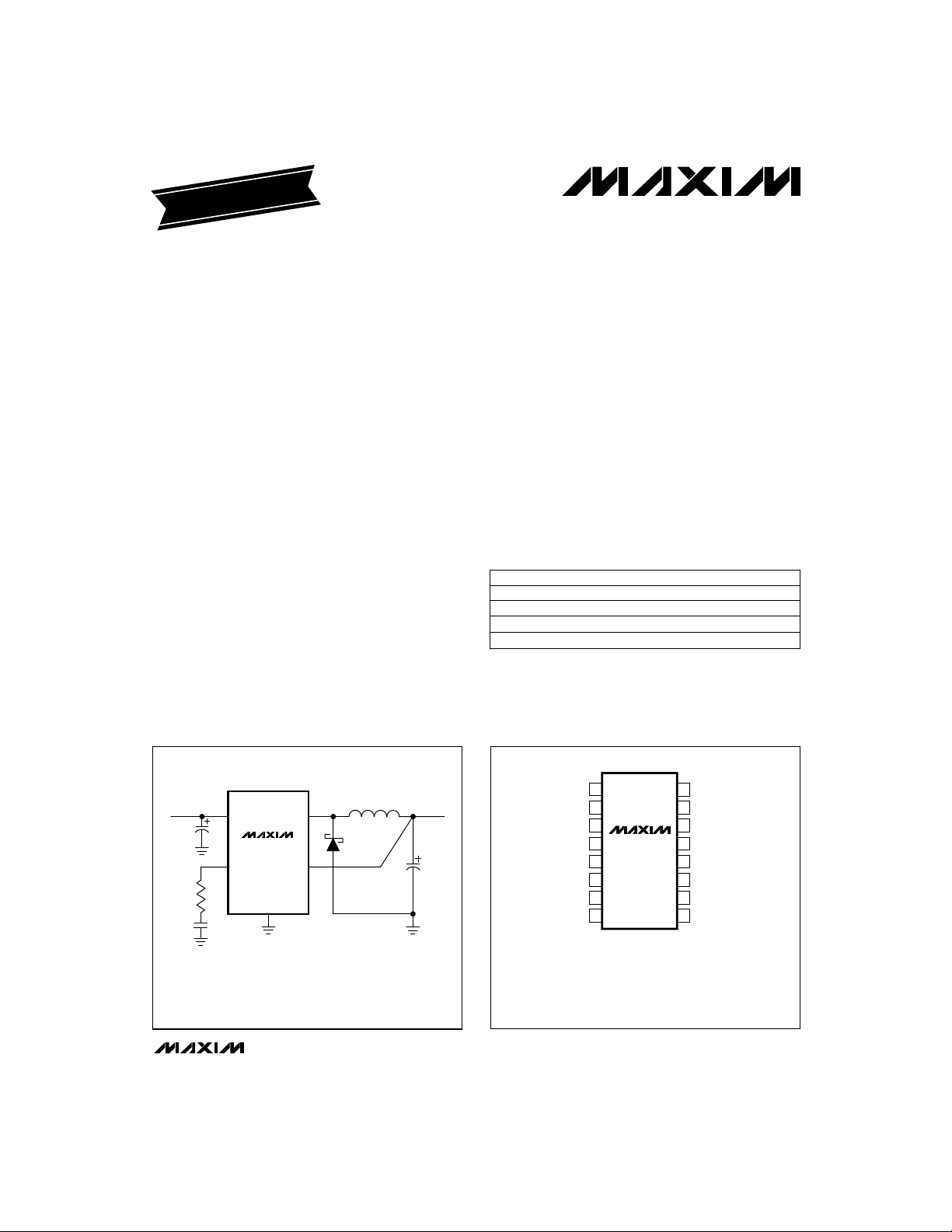
__________Typical Operating Circuit
INPUT
8V TO 30V
100µF
10k
0.047µF
* CoilCraft DO3316-104
V
V
IN
C
MAX831
GND
V
SENSE
SW
100µH*
MBR350
STEP-DOWN CONVERTER
________________________________________________________________
OUTPUT
5V AT 1A
470µF
__________________Pin Configuration
TOP VIEW
V
IN
1
V
2
IN
V
IN
3
V
IN
MAX830
4
GND
I
GND
(FB) SENSE
( ) ARE FOR MAX830
* THIS THERMAL RESISTANCE NUMBER IS WITH THE DEVICE WELL MOUNTED
ON 1 oz. COPPER WITH THERMAL PASTE BETWEEN THE IC AND THE
UNDERLYING GROUND PLANE. LOWER THERMAL RESISTANCE IS POSSIBLE
(SEE APPLICATIONS SECTION).
MAX831
5
MAX832
MAX833
6
LIM
7
8
Wide SO
Tj (
= +125°C, θ
MAX)
Maxim Integrated Products
Call toll free 1-800-998-8800 for free samples or literature.
jA =
V
SW
16
V
15
SW
V
14
SW
V
13
SW
GND
12
V
11
C
GND
10
SHUT
9
+55°C/W*
1
Page 2
5V/3.3V/3V/Adjustable-Output, 1A,
Step-Down, PWM, Switch-Mode DC-DC Regulators
ABSOLUTE MAXIMUM RATINGS
Input Voltage..................................................40V
Switch Voltage with Respect to Input Voltage................50V
Switch Voltage with Respect to GND
negative) (Note 1).....................................20V
(V
SW
FB/SENSE Voltage ...................................-0.3V, +10V
SHUT Voltage (not to exceed V
Note 1: Do not exceed switch-to-input voltage limitation.
Stresses beyond those listed under “Absolute Maximum Ratings” may cause permanent damage to the device. These are stress ratings only, and functional
operation of the device at these or any other conditions beyond those indicated in the operational sections of the specifications is not implied. Exposure to
absolute maximum rating conditions for extended periods may affect device reliability.
)............................30V
IN
ELECTRICAL CHARACTERISTICS
(VIN= 25V, TA= T
MAX830–MAX833
MAX830–MAX833
Input Supply Voltage Range 830V
Switch-On Voltage (Note 2)
Switch-Off Leakage
Supply Current (Note 3)
Minimum Supply Voltage (Note 5)
Switch-Current Limit (Note 6)
Maximum Duty Cycle
Switching Frequency
Switching-Frequency Line Regulation 8V ≤ VIN≤ 30V 0.03 0.10 %/V
Error-Amplifier Voltage Gain 1V ≤ VC≤ 4V 2000 V/V
Error-Amplifier Transconductance
Error-Amplifier Source Current
Error-Amplifier Sink Current
to T
MIN
PARAMETER CONDITIONS
, unless otherwise noted. Typical values are at TA = +25°C.)
MAX
ISW= 0.2A 1.1
ISW= 1A 1.4
VIN= 25V, VSW= 0V 150
VIN= 30V, VSW= 0V 250
VIN≤ 30V, V
MAX833) or V
V
= 0.1V (Note 4) 140 500 µA
SHUT
Normal mode
Startup mode 3.5 4.8
I
open
LIM
R
= 10kΩ (Note 7)
LIM
R
= 7kΩ (Note 7)
LIM
VFBor V
SENSE
VFB= 2.0V (MAX830) or
= 2.0V
V
SENSE
(MAX831/832/833)
VFB= 2.5V (MAX830) or
= 5.5V
V
SENSE
(MAX831/832/833)
= 5.5V (MAX831/MAX832/
SENSE
= 2.5V (MAX830)
FB
= 0V (Note 6)
Voltage (forced)..........................................5.5V
I
LIM
Operating Temperature Range.....................0°C to +70°C
Junction Temperature Range.....................0°C to +125°C
Storage Temperature Range ...................-65°C to +160°C
Lead Temperature (soldering, 10sec)....................+300°C
MIN TYP MAX UNITS
V
TA= +25°C
TA= +25°C
TA= +25°C
TA= +25°C
TA= +25°C
TA= +25°C
811
7.3 8.0
1.2 1.7 2.2
1.2
0.8
85 90 %
90 100 110
85 120
20
3000 5000 9000 µmho
100 140 225
0.6 1.0 1.7 mATA= +25°C
µA
mA
V
A
kHz
µATA= +25°C
2 _______________________________________________________________________________________
Page 3

5V/3.3V/3V/Adjustable-Output, 1A,
Step-Down, PWM, Switch-Mode DC-DC Regulators
ELECTRICAL CHARACTERISTICS (continued)
(VIN= 25V, TA= T
PARAMETER CONDITIONS
SENSE Voltage
FB Bias Current 0.5 2.0
Reference Voltage Tolerance
(Notes 8, 9)
VCVoltage Temperature Coefficient
SHUT Current
SHUT Threshold V
MIN
to T
, unless otherwise noted. Typical values are at TA = +25°C.)
MAX
VC= 2V
V
(nominal) = 5V (MAX831),
OUT
3.3V (MAX832), or 3V (MAX833)
VFB= V
VC= 2V (MAX830) (Note 9)
V
REF
8V ≤ VIN≤ 30V
0% duty cycle
0% duty cycle -4
V
SHUT
V
SHUT
(shutdown) 0.10 0.20 0.50
(MAX830)
REF
(nominal = 2.21V) (MAX830)
= 5V
= 0.1V (shutdown) 50
MAX831
MAX832
MAX833
MAX831
MAX832
MAX833
TA= +25°C
TA= +25°C 1.5VCVoltage
MIN TYP MAX UNIT
4.85 5.00 5.15
3.20 3.30 3.40
2.90 3.00 3.10
3.0 5.0 8.0
2.5 4.2 7.0SENSE Divider Resistance TA= +25°C
2.2 3.8 6.5
±0.5 ±2.0
±0.5 ±3.0
2.155 2.21 2.265
±0.5 ±1.5TA= +25°C
±1.0 ±2.5
0.005 0.020 %/VOutput Voltage Line Regulation
mV/°C
10 20
V
kΩ
%SENSE Voltage Tolerance (Note 8)
µA
VReference Voltage
%
V
µA
MAX830–MAX833
MAX830–MAX833
Note 2: For switch currents between 0.2A and 1A, maximum switch-on voltage can be calculated via linear interpolation.
Note 3: By setting the SENSE pin to 5.5V (or the FB pin to 2.5V), the V
is forced to zero, approximating the zero load condition.
Note 4: Device shut down. Switch leakage current not included.
Note 5: For proper regulation, total voltage from V
but not regulating.
Note 6: To avoid extremely short switch-on times, the switch frequency is internally scaled down when V
1.3V. Switch current limit is tested with V
I
LIM
R
Note 7:
Note 8: All conditions of input voltage, output voltage, temperature, and load current.
Note 9: FB is at the reference voltage when the MAX830 output voltage is in regulation.
=×
LIM
1A
7.6k 1k
_______________________________________________________________________________________ 3
Typical value only. Minimum to maximum deviation in current limit will be ±30%,
+ΩΩ .
comparable to that with I
to GND must be ≥ 8V after start-up. During start-up mode, device is switching
IN
or VFBadjusted to give a 1µs minimum switch-on time.
SENSE
pin is forced to its low clamp level and the switch duty cycle
C
or V
FB
pin open.
LIM
SENSE
is less than
Page 4

5V/3.3V/3V/Adjustable-Output, 1A,
Step-Down, PWM, Switch-Mode DC-DC Regulators
______________________________________________________________Pin Description
PIN FUNCTION
11
5, 7,
10, 12
13, 14,
MAX830–MAX833
MAX830–MAX833
15, 16
1, 2,
3, 4
__________Applications Information
Although the MAX830–MAX833 are high-efficiency
step-down voltage converters, certain precautions are
required to avoid excessive chip temperature (the
absolute maximum rating for this parameter, Tj, is
+125°C). The 16-pin SO package has thermal resistance of +55°C/W when mounted properly; this limits
continuous chip power dissipation to the 1W range.
When installing these chips:
1) Use wide and, if possible, thick copper traces to
connect the leads (especially the GND pins) to
reduce thermal resistance.
2) Bond the package firmly to the board or use a clipstyle heatsink. A very small drop of thermal paste
between the chip package and the copper ground
plane is also helpful.
3) Confirm that the range of device operation is such
that the chip temperature does not exceed the
allowed maximum of Tj= +125°C. This can be
determined from Tables 1 and 2.
Tables 1 and 2 show numbers for maximum allowed
load current based on not exceeding the Tj= +125°C
limit. If the input voltage range, ambient temperature,
and/or output voltage setting allow for an unsafe level
of load current, limit the load current to a safe value by
connecting the appropriate resistor from the I
GND. With no external resistor, the preset switch cur-
NAME
SENSE
(MAX831/
8
6
9 Shutdown is achieved by pulling SHUT low. Leave SHUT floating for normal operation.
2/3)
FB
(MAX830)
V
GND
V
V
I
LIM
SHUT
For the MAX831/MAX832/MAX833, SENSE input is the internal error amplifier’s input, and should be
directly connected to V
is low.
For the MAX830, the FB input is the internal error amplifier's input, and should be connected to the midpoint of a potential divider between V
be that value that forces 2.21V (V
Error-amplifier output. A series RC network connected to this pin compensates the device. Output swing
is limited to about 5.8V in the positive direction and -0.7V in the negative direction. V
C
nize the device to an external TTL clock in the 115kHz to 170kHz range.
Ground requires a short, low-noise connection to ensure good load regulation. The internal reference is referred
to GND, so errors at this pin are multiplied by the error amplifier. Use thick copper for low thermal resistance.
Internal power switch output (rated for 1A load current)
SW
VINsupplies power to the internal circuitry and also connects to the collector of the internal power switch.
IN
must be bypassed with a low-ESR capacitor, typically 100µF.
V
IN
Switch-current limit can be reduced by connecting an external resistor (R
(See Note 7 in
Electrical Characteristics
. SENSE also aids current limiting by reducing oscillator frequency when V
OUT
and GND (Figure 1). The output voltage, during regulation, will
OUT
) at the FB pin.
REF
) from I
). Leave I
floating for maximum current limit.
LIM
LIM
LIM
rent limit (typically 1.7A) will limit the load current to
about 1.3A. Table 1 shows safe operating load currents for the MAX830 for various values of input and
output voltage and at three different ambient temperatures of TA= +25°C, +45°C, and +70°C, respectively.
Table 2 shows the same information, but for the fixed
output voltage MAX831, MAX832, and MAX833.
When consulting these tables, note that power surges
of less than 30sec need not be considered from a thermal standpoint. It is important for proper regulation,
however, that a power surge not require a peak switch
current exceeding the 1.2A (min) switch current limit.
Also, the inductor’s current rating should exceed I
For highest efficiency, the inductor series resistance
should be 0.4Ω or less. I
PEAK
and I
the following formula:
[V
x (V
I
PEAK
= I
LOAD
OUT
+ ——————————
VINx L x 200,000
Example: MAX830 with VIN= 30V, V
I
= 0.5A continuous, L = 100µH and
LOAD
TA= +70°C:
I
= 0.86A (which is below 1.2A (min)
PEAK
preset switch current limit);
and from Table 1:
LIM
pin to
maximum I
(i.e., operation is safe).
allowed = 0.8A continuous
LOAD
can also synchro-
C
to GND
are related by
LOAD
- V
IN
OUT
)]
OUT
= 15V,
OUT
PEAK
.
4 _______________________________________________________________________________________
Page 5

5V/3.3V/3V/Adjustable-Output, 1A,
q
q
Step-Down, PWM, Switch-Mode DC-DC Regulators
Table 1. MAX830 Maximum Load Current (continuous with
Output Voltage and Ambient Temperature
OUTPUT VOLTAGE
Up to 10V 1A 1A 1A
10V to 15V 1A 1A 0.8A
15V to 20V 1A 0.8A 0.7A
20V to 25V 0.8A 0.7A 0.6A
TA= +25°C TA= +45°C TA= +70°C
CONTINUOUS LOAD CURRENT
Table 2. MAX831/MAX832/MAX833 Maximum Load Current (continuous with
= +55°C/W) vs. Ambient Temperature
jA
OUTPUT VOLTAGE
Fixed:
5V, 3.3V or 3V
TA= +25°C TA= +45°C TA= +70°C
1A 1A 1A
CONTINUOUS LOAD CURRENT
= +55°C/W) vs.
jA
MAX830–MAX833
INPUT
UP TO 30V
100µF
10k
Figure 1. MAX830 Typical Operating Circuit
_________________________________________________________________________________________________
_______________________________________________________________________________________ 5
V
MAX830
GND
SW
FB
V
IN
V
C
0.047µF
STEP-DOWN CONVERTER
100µH
MBR350
R1
=
1 +
V
OUT
[
R2
]
R1
R2
x 2.21V
V
OUT
470µF
5
 Loading...