Page 1

General Description
The ultra-small MAX828/MAX829 monolithic, CMOS
charge-pump inverters accept input voltages ranging
from +1.5V to +5.5V. The MAX828 operates at 12kHz,
and the MAX829 operates at 35kHz. Their high efficiency
(greater than 90% over most of the load-current range)
and low operating current (60µA for the MAX828) make
these devices ideal for both battery-powered and boardlevel voltage-conversion applications.
The MAX828/MAX829 combine low quiescent current
and high efficiency. Oscillator control circuitry and four
power MOSFET switches are included on-chip.
Applications include generating a -5V supply from a +5V
logic supply to power analog circuitry. Both parts come
in a 5-pin SOT23-5 package and can deliver 25mA with
a voltage drop of 500mV.
For a similar device with logic-controlled shutdown,
refer to the MAX1719/MAX1720/MAX1721. For applications requiring more power, the MAX860 delivers up to
50mA with a voltage drop of 600mV, in a space-saving
µMAX package.
Applications
Small LCD Panels
Cell Phones
Medical Instruments
Handy-Terminals, PDAs
Battery-Operated Equipment
Features
♦ 5-Pin SOT23-5 Package
♦ 95% Voltage Conversion Efficiency
♦ Inverts Input Supply Voltage
♦ 60µA Quiescent Current (MAX828)
♦ +1.5V to +5.5V Input Voltage Range
♦ Requires Only Two Capacitors
♦ 25mA Output Current
MAX828/MAX829
Switched-Capacitor Voltage Inverters
________________________________________________________________ Maxim Integrated Products 1
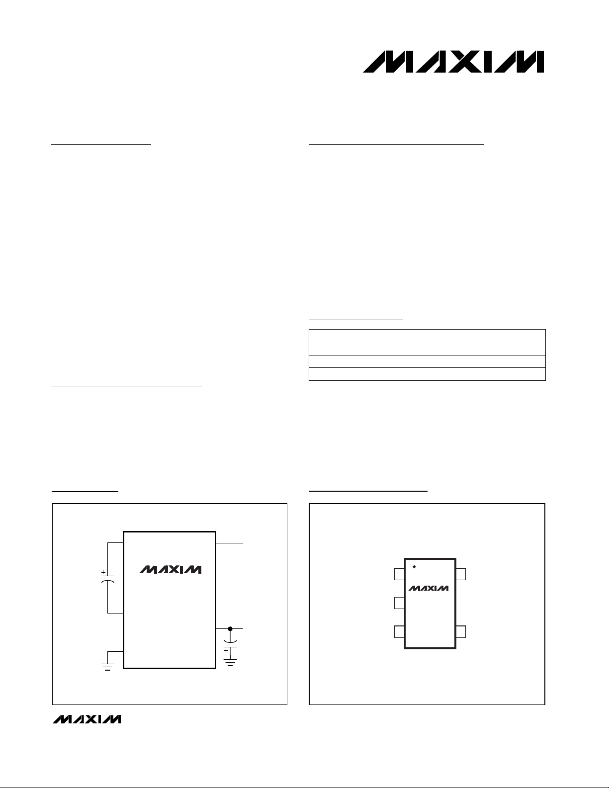
Pin Configuration
NEGATIVE VOLTAGE CONVERTER
C1+
C1-
IN
OUT
GND
INPUT
SUPPLY
VOLTAGE
NEGATIVE
OUTPUT
VOLTAGE
MAX828
MAX829
4
3
52
1
Typical Operating Circuit
19-0495; Rev 3; 9/99
PART
MAX828EUK
-40°C to +85°C
TEMP. RANGE
PIN-
PACKAGE
5 SOT23-5
Ordering Information
MAX829EUK
-40°C to +85°C 5 SOT23-5
SOT
TOP MARK
AABI
AABJ
For price, delivery, and to place orders, please contact Maxim Distribution at 1-888-629-4642,
or visit Maxim’s website at www.maxim-ic.com.
TOP VIEW
OUT
IN
C1-
1
2
3
MAX828
MAX829
SOT23-5
C1+
5
GND
4
Page 2

MAX828/MAX829
Switched-Capacitor Voltage Inverters
2 _______________________________________________________________________________________
ABSOLUTE MAXIMUM RATINGS
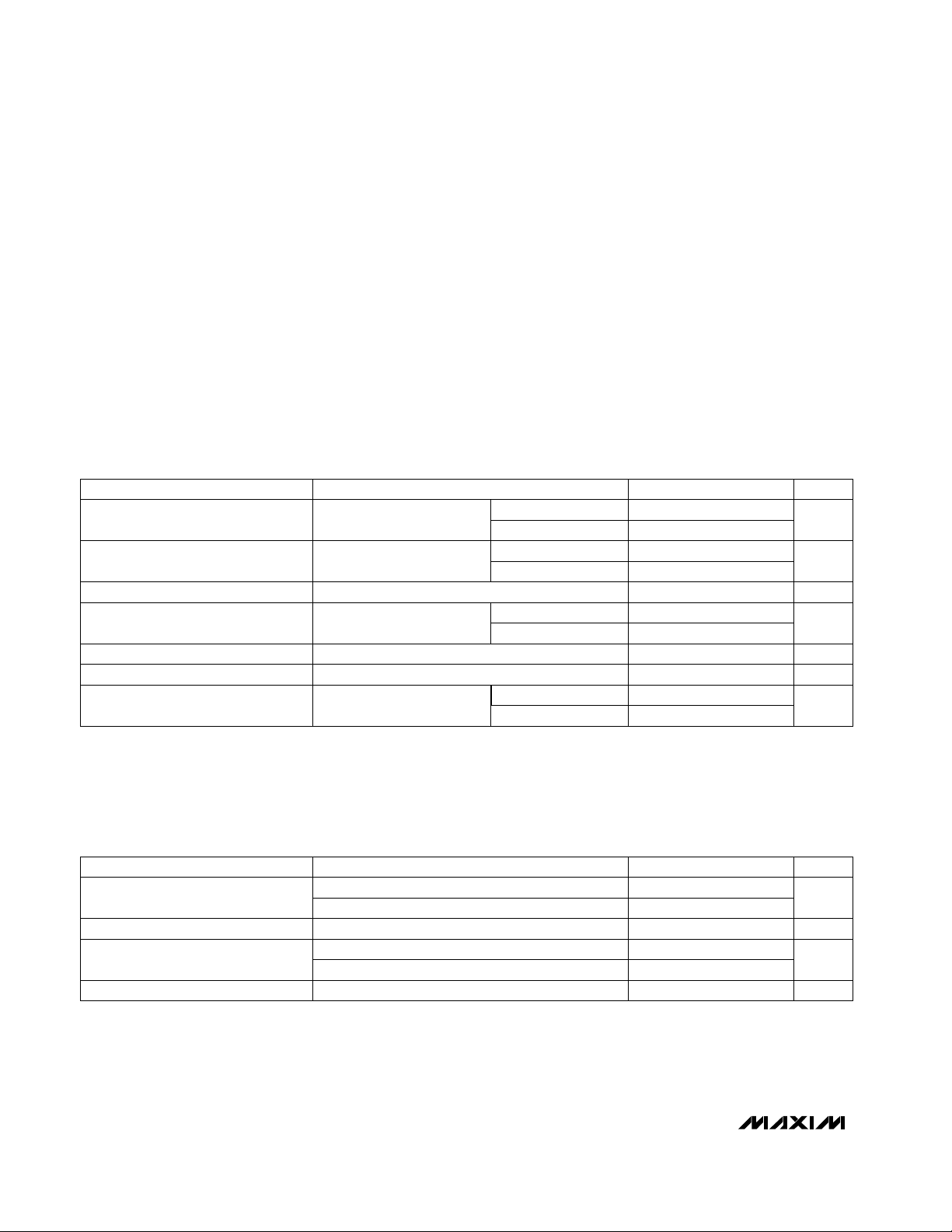
ELECTRICAL CHARACTERISTICS
(VIN= +5V, C1 = C2 = 10µF (MAX828), C1 = C2 = 3.3µF (MAX829), TA= 0°C to +85°C, unless otherwise noted. Typical values
are at T
A
= +25°C.)
ELECTRICAL CHARACTERISTICS
(VIN= +5V, C1 = C2 = 10µF (MAX828), C1 = C2 = 3.3µF (MAX829), TA= -40°C to +85°C, unless otherwise noted. Typical values
are at T
A
= +25°C.) (Note 2)
Stresses beyond those listed under “Absolute Maximum Ratings” may cause permanent damage to the device. These are stress ratings only, and functional
operation of the device at these or any other conditions beyond those indicated in the operational sections of the specifications is not implied. Exposure to
absolute maximum rating conditions for extended periods may affect device reliability.
Note 1: Capacitor contribution is approximately 20% of the output impedance [ESR + 1 / (pump frequency x capacitance)].
Note 2: All -40°C to +85°C specifications above are guaranteed by design.
IN to GND .................................................................+6.0V, -0.3V
OUT to GND .............................................................-6.0V, +0.3V
OUT Output Current ...........................................................50mA
OUT Short-Circuit to GND ............................................Indefinite
Continuous Power Dissipation (T
A
= +70°C)
SOT23-5 (derate 7.1mW/°C above +70°C)...................571mW
Operating Temperature Range
MAX828EUK/MAX829EUK ...............................-40°C to +85°C
Storage Temperature Range .............................-65°C to +160°C
Lead Temperature (soldering, 10s) .................................+300°C
MAX829
MAX828
R
LOAD
= ∞
R
LOAD
= 1kΩ, TA= +25°C
MAX829
R
LOAD
= 10kΩ
R
LOAD
= 10kΩ
MAX828
CONDITIONS
µA
150 260
60 90
Supply Current
%95 99.9Voltage Conversion Efficiency
%94Power Efficiency
kHz
24.5 35 45.5
Oscillator Frequency
1.25 1.0
V
1.5
Minimum Supply Voltage
V5.5Maximum Supply Voltage
8.4 12 15.6
UNITSMIN TYP MAXPARAMETER
TA= +25°C
TA= 0°C to + 85°C
I
OUT
= 5mA
TA= 0°C to + 85°C
TA= +25°C
Ω
65
Output Resistance
20 50
MAX829
MAX828
I
OUT
= 5mA
MAX829
R
LOAD
= 10kΩ
MAX828
CONDITIONS
µA
325
115
Supply Current
Ω65Output Resistance
kHz
19 54.3
Oscillator Frequency
V1.5 5.5Supply Voltage Range
620
UNITSMIN TYP MAXPARAMETER
TA= +25°C
TA= +25°C
Page 3

MAX828/MAX829
Switched-Capacitor Voltage Inverters
_______________________________________________________________________________________ 3
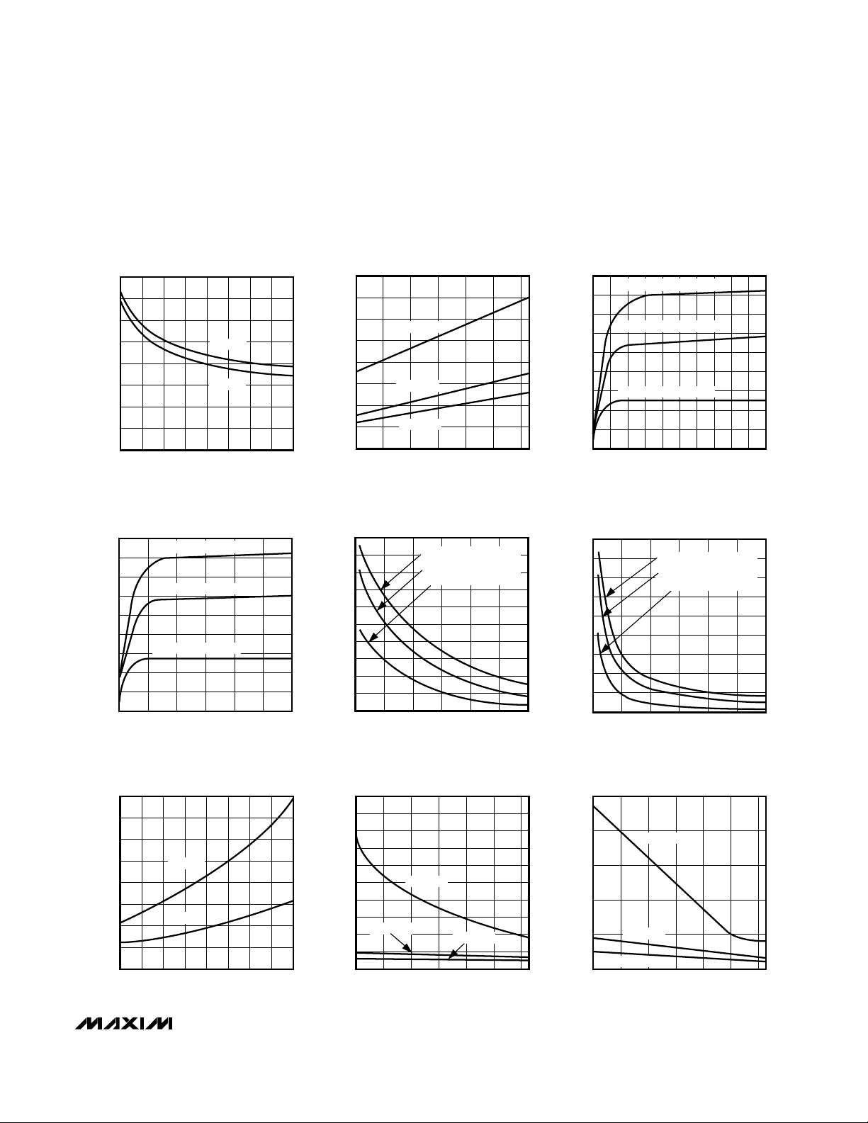
__________________________________________Typical Operating Characteristics
(Circuit of Figure 1, VIN= +5V, C1 = C2 = C3, TA= +25°C, unless otherwise noted.)
OUTPUT RESISTANCE
vs. SUPPLY VOLTAGE
MAX828/829-01
50
45
40
35
30
25
20
OUTPUT RESISTANCE (Ω)
15
10
-40 -20 0 6020 40 80
40
35
30
25
20
15
10
OUTPUT RESISTANCE (Ω)
5
0
1.5 2.5
MAX829
MAX828
3.5 5.54.5
SUPPLY VOLTAGE (V)
MAX829
OUTPUT CURRENT vs. CAPACITANCE
45
40
35
30
25
20
15
OUTPUT CURRENT (mA)
10
5
0
VIN = 4.75V, V- = -4.0V
VIN = 3.15V, V- = -2.5V
VIN = 1.9V, V- = -1.5V
0 5 20 25
CAPACITANCE (µF)
1510 30
500
450
MAX828/829-04
400
350
300
250
200
150
100
OUTPUT VOLTAGE RIPPLE (mVp-p)
50
0
0 5 20 25
OUTPUT RESISTANCE
vs. TEMPERATURE
VIN = 1.5V
VIN = 3.3V
VIN = 5.0V
TEMPERATURE (°C)
MAX828
OUTPUT VOLTAGE RIPPLE
vs. CAPACITANCE
VIN = 4.75V, V
V
IN
V
IN
CAPACITANCE (µF)
OUT
= 3.15V, V
OUT
= 1.9V, V
1510 30
OUT
= -1.5V
= -4.0V
= -2.5V
OUTPUT CURRENT vs. CAPACITANCE
45
40
MAX828/829-02
35
30
25
20
15
OUTPUT CURRENT (mA)
10
VIN = 4.75V, V
VIN = 3.15V, V
VIN = 1.9V, V
5
0
010515 3540
OUTPUT VOLTAGE RIPPLE
vs. CAPACITANCE
450
400
MAX828/829-05
350
300
250
200
150
100
OUTPUT VOLTAGE RIPPLE (mVp-p)
50
0
0 5 20 25
MAX828
= -4.0V
OUT
= -2.5V
OUT
= -1.5V
OUT
20 25 30 45 50
CAPACITANCE (µF)
MAX829
VIN = 4.75V, V
V
= 3.15V, V
IN
V
= 1.9V, V
IN
1510 30
CAPACITANCE (µF)
OUT
OUT
OUT
= -4.0V
= -2.5V
= -1.5V
MAX828/829-03
MAX828/829-06
200
175
150
125
100
75
SUPPLY CURRENT (µA)
50
25
0
1.5 2.5
SUPPLY CURRENT
vs. SUPPLY VOLTAGE
MAX829
MAX828
3.5 5.54.5
SUPPLY VOLTAGE (V)
PUMP FREQUENCY vs. TEMPERATURE
60
55
MAX828/829-07
50
45
40
35
30
25
PUMP FREQUENCY (kHz)
20
15
10
-40 -20 0 60
VIN = 3.3V
MAX828
VIN = 1.5V
VIN = 5.0V
20 40 80
TEMPERATURE (°C)
PUMP FREQUENCY vs. TEMPERATURE
55
MAX828/829-08
50
45
40
PUMP FREQUENCY (kHz)
35
30
-40 -20 0 6020 40 80
MAX829
VIN = 1.5V
VIN = 3.3V
VIN = 5.0V
TEMPERATURE (°C)
MAX828/829-9
Page 4

_____________________Pin Description
MAX828/MAX829
Switched-Capacitor Voltage Inverters
4 _______________________________________________________________________________________
Typical Operating Characteristics (continued)
(Circuit of Figure 1, VIN= +5V, C1 = C2 = C3, TA= +25°C, unless otherwise noted.)
0.5
-5.5
05 1510 35
OUTPUT VOLTAGE
vs. OUTPUT CURRENT
-4.5
-0.5
MAX828/829-10
OUTPUT CURRENT (mA)
OUTPUT VOLTAGE (V)
20 3025 45 5040
-1.5
-2.5
-3.5
VIN = 3.3V
VIN = 5.0V
VIN = 2.0V
100
0
0510
EFFICIENCY vs. OUTPUT CURRENT
10
30
20
90
MAX828/829-11
OUTPUT CURRENT (mA)
EFFICIENCY (%)
2015 3025 4540 5035
70
80
50
60
40
VIN = 2.0V
VIN = 3.3V
V
IN
= 5.0V
V
OUT
20mV/div
MAX828
OUTPUT NOISE AND RIPPLE
MAX828/829-12
V
IN
= 3.3V, V
OUT
= -3.2V, I
OUT
= 5mA, AC COUPLED
20µs/div
Flying Capacitor’s Positive TerminalC1+5
GroundGND4
Flying Capacitor’s Negative TerminalC1-3
PIN
Positive Power-Supply InputIN2
Inverting Charge-Pump OutputOUT
1
FUNCTIONNAME
Figure 1. Test Circuit
V
OUT
20mV/div
MAX829
OUTPUT NOISE AND RIPPLE
MAX828/829-13
V
IN
= 3.3V, V
OUT
= -3.2V, I
OUT
= 5mA, AC COUPLED
10µs/div
V
C1
3.3µF*
IN
V
OUT
R
L
C3
3.3µF*
1
OUT
2
MAX828
IN
C1+
5
C2
3.3µF*
MAX829
3
*10µF
(MAX828)
4
GNDC1-
VOLTAGE INVERTER
Page 5

_______________Detailed Description
The MAX828/MAX829 capacitive charge pumps invert the
voltage applied to their input. For highest performance,
use low equivalent series resistance (ESR) capacitors.
During the first half-cycle, switches S2 and S4 open,
switches S1 and S3 close, and capacitor C1 charges to
the voltage at IN (Figure 2). During the second halfcycle, S1 and S3 open, S2 and S4 close, and C1 is level
shifted downward by VINvolts. This connects C1 in parallel with the reservoir capacitor C2. If the voltage across
C2 is smaller than the voltage across C1, then charge
flows from C1 to C2 until the voltage across C2 reaches VIN. The actual voltage at the output is more positive
than -VIN, since switches S1–S4 have resistance and the
load drains charge from C2.
Charge-Pump Output
The MAX828/MAX829 are not voltage regulators: the
charge pump’s output source resistance is approximately 20Ω at room temperature (with VIN= +5V), and
V
OUT
approaches -5V when lightly loaded. V
OUT
will
droop toward GND as load current increases. The
droop of the negative supply (V
DROOP-
) equals the cur-
rent draw from OUT (I
OUT
) times the negative convert-
er’s source resistance (RS-):
V
DROOP-
= I
OUT
x RS-
The negative output voltage will be:
V
OUT
= -(VIN- V
DROOP-
)
Efficiency Considerations
The efficiency of the MAX828/MAX829 is dominated by
its quiescent supply current (IQ) at low output current
and by its output impedance (R
OUT
) at higher output
current; it is given by:
where the output impedance is roughly approximated
by:
The first term is the effective resistance of an ideal
switched-capacitor circuit (Figures 3a and 3b), and
R
SW
is the sum of the charge pump’s internal switch
resistances (typically 8Ω to 9Ω at VIN= +5V). The typical
output impedance is more accurately determined from
the Typical Operating Characteristics.
Applications Information
Capacitor Selection
To maintain the lowest output resistance, use capacitors
with low ESR (Table 1). The charge-pump output resistance is a function of C1’s and C2’s ESR. Therefore,
minimizing the charge-pump capacitor’s ESR minimizes
the total output resistance.
R
1
f x C1
2R 4ESR ESR
OUT
OSC
SW C1 C2
≅
()
++ +
I
II
1
I x R
V
OUT
OUT Q
OUT OUT
IN
η≅
+
−
MAX828/MAX829
Switched-Capacitor Voltage Inverters
_______________________________________________________________________________________ 5
Figure 2. Ideal Voltage Inverter
Figure 3a. Switched-Capacitor Model
R
EQUIV
=
R
EQUIV
V
OUT
R
L
1
V+
f × C1
C2
Figure 3b. Equivalent Circuit
IN
S1
C1
S3 S4
S2
C2
V
= -(VIN)
OUT
f
V+
C1
C2 R
V
OUT
L
Page 6

MAX828/MAX829
Switched-Capacitor Voltage Inverters
6 _______________________________________________________________________________________
Flying Capacitor (C1)
Increasing the flying capacitor’s size reduces the output
resistance. Small C1 values increase the output resistance. Above a certain point, increasing C1’s capacitance has a negligible effect, because the output
resistance becomes dominated by the internal switch
resistance and capacitor ESR.
Output Capacitor (C2)
Increasing the output capacitor’s size reduces the output
ripple voltage. Decreasing its ESR reduces both output
resistance and ripple. Smaller capacitance values can
be used with light loads if higher output ripple can be
tolerated. Use the following equation to calculate the
peak-to-peak ripple:
Input Bypass Capacitor
Bypass the incoming supply to reduce its AC impedance
and the impact of the MAX828/MAX829’s switching noise.
The recommended bypassing depends on the circuit
configuration and on where the load is connected.
When the inverter is loaded from OUT to GND, current
from the supply switches between 2 x I
OUT
and zero.
Therefore, use a large bypass capacitor (e.g., equal to
the value of C1) if the supply has a high AC impedance.
When the inverter is loaded from IN to OUT, the circuit
draws 2 x I
OUT
constantly, except for short switching
spikes. A 0.1µF bypass capacitor is sufficient.
Voltage Inverter
The most common application for these devices is a
charge-pump voltage inverter (Figure 1). This application
requires only two external components—capacitors C1
and C2—plus a bypass capacitor, if necessary. Refer to
the Capacitor Selection section for suggested capacitor
types and values.
Cascading Devices
Two devices can be cascaded to produce an even
larger negative voltage (Figure 4). The unloaded output
voltage is normally -2 x VIN, but this is reduced slightly
by the output resistance of the first device multiplied by
the quiescent current of the second. When cascading
more than two devices, the output resistance rises dramatically. For applications requiring larger negative
voltages, see the MAX864 and MAX865 data sheets.
Paralleling Devices
Paralleling multiple MAX828s or MAX829s reduces the
output resistance. Each device requires its own pump
capacitor (C1), but the reservoir capacitor (C2) serves
all devices (Figure 5). Increase C2’s value by a factor
of n, where n is the number of parallel devices. The
equation for calculating output resistance is also shown
in Figure 5.
Combined Doubler/Inverter
In the circuit of Figure 6, capacitors C1 and C2 form the
inverter, while C3 and C4 form the doubler. C1 and C3
are the pump capacitors; C2 and C4 are the reservoir
capacitors. Because both the inverter and doubler use
part of the charge-pump circuit, loading either output
causes both outputs to decline toward GND. Make sure
the sum of the currents drawn from the two outputs
does not exceed 40mA.
Table 1. Low-ESR Capacitor Manufacturers
Matsuo
AVX
MANUFACTURER
(714) 969-2491
(803) 946-0690
(800) 282-4975
PHONE
(603) 224-1961
(619) 661-6835
Sprague
Sanyo
(603) 224-1430
(619) 661-1055
(714) 960-6492
(803) 626-3123
FAX
Surface-mount, 595D series
Through-hole, OS-CON series
Surface-mount, 267 series
Surface-mount, TPS series
DEVICE TYPE
USA
Japan 81-7-2070-6306 81-7-2070-1174
V =
RIPPLE
I
OUT
f x C2
OSC
+ 22x I x ESR
OUT C
Page 7

MAX828/MAX829
Switched-Capacitor Voltage Inverters
_______________________________________________________________________________________ 7
Heavy Output Current Loads
When under heavy loads, where higher supply is sourcing
current into OUT, the OUT supply must not be pulled
above ground. Applications that sink heavy current into
OUT require a Schottky diode (1N5817) between GND
and OUT, with the anode connected to OUT (Figure 7).
Layout and Grounding
Good layout is important, primarily for good noise performance. To ensure good layout, mount all components as
close together as possible, keep traces short to minimize parasitic inductance and capacitance, and use a
ground plane.
Shutting Down the MAX828/MAX829
For a similar device with logic-controlled shutdown,
please refer to the MAX1719/MAX1720/MAX1721. To
add manual shutdown control to the MAX828/MAX829,
use the circuit in Figure 8. The output resistance of the
MAX828/MAX829 will typically be 20Ω plus two times
the output resistance of the buffer driving IN. The 0.1µF
capacitor at the IN pin absorbs the transient input currents of the MAX828/MAX829.
The output resistance of the buffer driving the IN pin can
be reduced by connecting multiple buffers in parallel.
The polarity of the SHUTDOWN signal can also be
changed by using a noninverting buffer to drive IN.
Figure 4. Cascading MAX828s or MAX829s to Increase
Output Voltage
Figure 5. Paralleling MAX828s or MAX829s to Reduce Output
Resistance
Figure 6. Combined Doubler and Inverter
Figure 7. High V- Load Current
…
+V
IN
2
33
44
C1
MAX828
MAX829
551
“1”
C1
MAX828
MAX829
“n”
2
1
…
C2
= -nV
V
OUT
IN
+V
IN
3
C1
4
MAX828
MAX829
5
2
1
C3
D1
D2
D1, D2 = 1N4148
= -V
V
OUT
C2
V
= (2VIN) -
OUT
(V
) - (V
FD1
C4
OF SINGLE DEVICE
R
OUT
R
=
OUT
NUMBER OF DEVICES
…
+V
IN
2
3
V
OUT
C2
C1
MAX828
44
MAX829
“1”
5
C1
3
MAX828
MAX829
51
“n”
2
V
OUT
1
…
V
= -V
OUT
IN
4
GND
IN
)
FD2
MAX828
MAX829
OUT
1
C2
Page 8

MAX828/MAX829
Switched-Capacitor Voltage Inverters
Figure 8. Shutdown Control
Maxim cannot assume responsibility for use of any circuitry other than circuitry entirely embodied in a Maxim product. No circuit patent licenses are
implied. Maxim reserves the right to change the circuitry and specifications without notice at any time.
8 _____________________Maxim Integrated Products, 120 San Gabriel Drive, Sunnyvale, CA 94086 408-737-7600
© 1999 Maxim Integrated Products Printed USA is a registered trademark of Maxim Integrated Products.
Package Information
Chip Information
TRANSISTOR COUNT: 58
SUBSTRATE CONNECTED TO IN
INPUT
OUT
2
IN
C
IN
0.1µF
1
OUTPUT
C2
3
C1-
C1
MAX828
5
MAX829
C1+
4
GND
SHUTDOWN
LOGIC
SIGNAL
ON
OFF
SOT5L.EPS
 Loading...