

Page 1
_______________General Description
The MAX796/MAX797/MAX799 high-performance, stepdown DC-DC converters with single or dual outputs
provide main CPU power in battery-powered systems.
These buck controllers achieve 96% efficiency by using
synchronous rectification and Maxim’s proprietary Idle
Mode™ control scheme to extend battery life at full-load
(up to 10A) and no-load outputs. Excellent dynamic
response corrects output transients caused by the latest
dynamic-clock CPUs within five 300kHz clock cycles.
Unique bootstrap circuitry drives inexpensive N-channel
MOSFETs, reducing system cost and eliminating the
crowbar switching currents found in some PMOS/NMOS
switch designs.
The MAX796/MAX799 are specially equipped with a secondary feedback input (SECFB) for transformer-based
dual-output applications. This secondary feedback path
improves cross-regulation of positive (MAX796) or negative (MAX799) auxiliary outputs.
The MAX797 has a logic-controlled and synchronizable
fixed-frequency pulse-width-modulating (PWM) operating
mode, which reduces noise and RF interference in sensitive mobile-communications and pen-entry applications.
The SKIP override input allows automatic switchover to
idle-mode operation (for high-efficiency pulse skipping) at
light loads, or forces fixed-frequency mode for lowest noise
at all loads.
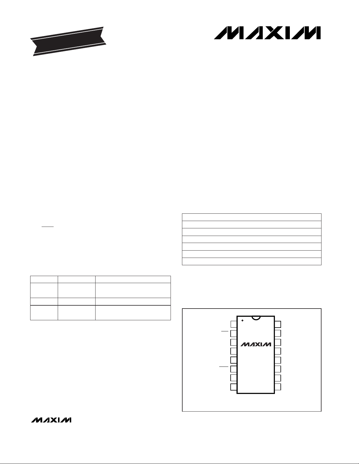
The MAX796/MAX797/MAX799 are all available in 16pin DIP and narrow SO packages. See the table below
to compare these three converters.
________________________Applications
Notebook and Subnotebook Computers
PDAs and Mobile Communicators
Cellular Phones
____________________________Features
♦ 96% Efficiency
♦ 4.5V to 30V Input Range
♦ 2.5V to 6V Adjustable Output
♦ Preset 3.3V and 5V Outputs (at up to 10A)
♦ Multiple Regulated Outputs
♦ +5V Linear-Regulator Output
♦ Precision 2.505V Reference Output
♦ Automatic Bootstrap Circuit
♦ 150kHz/300kHz Fixed-Frequency PWM Operation
♦ Programmable Soft-Start
♦ 375µA Typ Quiescent Current (VIN= 12V, V
OUT
= 5V)
♦ 1µA Typ Shutdown Current
MAX796/MAX797/MAX799
Step-Down Controllers with
Synchronous Rectifier for CPU Power
________________________________________________________________
Maxim Integrated Products
1
PART
MAX799
MAIN OUTPUT SPECIAL FEATURE
3.3V/5V or adj.
Regulates negative secondary
voltage (such as -5V)
MAX797 3.3V/5V or adj. Logic-controlled low-noise mode
MAX796 3.3V/5V or adj.
Regulates positive secondary
voltage (such as +12V)
Idle Mode is a trademark of Maxim Integrated Products.
†
U.S. and foreign patents pending.
19-0221; Rev 3a; 11/97
EVALUATION KIT MANUALS
FOLLOW DATA SHEET
__________________Pin Configuration
16
15
14
13
12
11
10
9
1
2
3
4
5
6
7
8
DH
LX
BST
DL
GND
REF
(SECFB) SKIP
SS
TOP VIEW
MAX796
MAX797
MAX799
PGND
VL
V+
CSL
( ) ARE FOR MAX796/ MAX799.
CSH
FB
SHDN
SYNC
DIP/SO
Dice*
16 Narrow SO
16 Plastic DIP
PIN-PACKAGETEMP. RANGE
0°C to +70°C
0°C to +70°C
0°C to +70°CMAX796C/D
MAX796CSE
MAX796CPE
PART
†
16 CERDIP
16 Narrow SO
16 Plastic DIP-40°C to +85°C
-40°C to +85°C
-55°C to +125°CMAX796MJE
MAX796ESE
MAX796EPE
Ordering Information continued at end of data sheet.
*Contact factory for dice specifications.
______________Ordering Information
For free samples & the latest literature: http://www.maxim-ic.com, or phone 1-800-998-8800.
For small orders, phone 408-737-7600 ext. 3468.
Page 2
MAX796/MAX797/MAX799
Step-Down Controllers with
Synchronous Rectifier for CPU Power
2 _______________________________________________________________________________________
ABSOLUTE MAXIMUM RATINGS
ELECTRICAL CHARACTERISTICS
(V+ = 15V, GND = PGND = 0V, IVL= I
REF
= 0A, TA= 0°C to +70°C for MAX79_C, TA= 0°C to +85°C for MAX79_E,
T
A
= -55°C to +125°C for MAX79_M, unless otherwise noted.)
Stresses beyond those listed under “Absolute Maximum Ratings” may cause permanent damage to the device. These are stress ratings only, and functional
operation of the device at these or any other conditions beyond those indicated in the operational sections of the specifications is not implied. Exposure to
absolute maximum rating conditions for extended periods may affect device reliability.
V+ to GND.................................................................-0.3V, +36V
GND to PGND........................................................................±2V
VL to GND ...................................................................-0.3V, +7V
BST to GND...............................................................-0.3V, +36V
DH to LX...........................................................-0.3V, BST + 0.3V
LX to BST.....................................................................-7V, +0.3V
SHDN
to GND............................................................-0.3V, +36V
SYNC, SS, REF, FB, SECFB, SKIP
, DL to GND..-0.3V, VL + 0.3V
CSH, CSL to GND .......................................................-0.3V, +7V
VL Short Circuit to GND..............................................Momentary
REF Short Circuit to GND...........................................Continuous
VL Output Current...............................................................50mA
Continuous Power Dissipation (T
A
= +70°C)
SO (derate 8.70mW/°C above +70°C)........................696mW
Plastic DIP (derate 10.53mW/°C above +70°C) .........842mW
CERDIP (derate 10.00mW/°C above +70°C)..............800mW
Operating Temperature Ranges
MAX79_C_ _ ......................................................0°C to +70°C
MAX79_E_ _....................................................-40°C to +85°C
MAX79_MJE .................................................-55°C to +125°C
Storage Temperature Range.............................-65°C to +160°C
Lead Temperature (soldering, 10sec).............................+300°C
Rising edge, hysteresis = 25mV
Rising edge, hysteresis = 15mV
SHDN = 2V, 0mA < IVL< 25mA, 5.5V < V+ < 30V
Falling edge, hysteresis = 20mV (MAX799)
CSH-CSL, negative
CSH-CSL, positive
Falling edge, hysteresis = 15mV (MAX796)
6V < V+ < 30V
25mV < (CSH-CSL) < 80mV
0mV < (CSH-CSL) < 80mV, FB = VL, 6V < V+ < 30V,
includes line and load regulation
External resistor divider
(CSH-CSL) = 0V
0mV < (CSH-CSL) < 80mV
CONDITIONS
V4.2 4.7VL/CSL Switchover Voltage
V3.8 4.1VL Fault Lockout Voltage
V4.7 5.3VL Output Voltage
-0.05 0 0.05
V
2.45 2.505 2.55
SECFB Regulation Setpoint
mA2.0SS Fault Sink Current
µA2.5 4.0 6.5SS Source Current
5.0 30
V
4.5 30
Input Supply Range
-50 -100 -160
mV
80 100 120
Current-Limit Voltage
%/V0.04 0.06Line Regulation
1.5
V4.85 5.10 5.255V Output Voltage (CSL)
VREF 6
Nominal Adjustable Output
Voltage Range
V2.43 2.505 2.57Feedback Voltage
%
2.5
Load Regulation
UNITSMIN TYP MAXPARAMETER
MAX79_C
MAX79_E/M
0mV < (CSH-CSL) < 80mV, FB = 0V, 4.5V < V+ < 30V,
includes line and load regulation
V3.20 3.35 3.463.3V Output Voltage (CSL)
+3.3V AND +5V STEP-DOWN CONTROLLERS
FLYBACK/PWM CONTROLLER
INTERNAL REGULATOR AND REFERENCE
Page 3
MAX796/MAX797/MAX799
Step-Down Controllers with
Synchronous Rectifier for CPU Power
_______________________________________________________________________________________ 3
Note 1: Since the reference uses VL as its supply, V+ line-regulation error is insignificant.
Note 2: At very low input voltages, quiescent supply current may increase due to excess PNP base current in the VL linear
regulator. This occurs only if V+ falls below the preset VL regulation point (5V nominal). See the Quiescent Supply Current
vs. Supply Voltage graph in the
Typical Operating Characteristics
.
ELECTRICAL CHARACTERISTICS (continued)
(V+ = 15V, GND = PGND = 0V, IVL= I
REF
= 0A, TA= 0°C to +70°C for MAX79_C, TA= 0°C to +85°C for MAX79_E,
T
A
= -55°C to +125°C for MAX79_M, unless otherwise noted.)
SECFB, 0V or 4V
SHDN, 0V or 30V
SHDN, SKIP
SYNC
SYNC = 0V or 5V
No external load (Note 1)
SYNC = REF
Guaranteed by design
CSH = CSL = 6V
V+ = 4V, CSL = 0V (Note 2)
SYNC = 0V or 5V
SHDN = 0V, V+ = 30V,
CSL = 0V or 6V
Falling edge
0µA < I
REF
< 100µA
SYNC = REF
SHDN = 0V, CSL = 6V, V+ = 0V or 30V, VL = 0V
CONDITIONS
0.1
MAX79_C
µA
2.0
MAX79_E/M
Input Current
2.0
V
VL - 0.5
Input High Voltage
%
93 96
89 91
Maximum Duty Cycle
kHz190 340Oscillator Sync Range
ns200SYNC Rise/Fall Time
ns200SYNC Low Pulse Width
ns200SYNC High Pulse Width
125 150 175
kHz
270 300 330
Oscillator Frequency
2.45 2.55
V
2.46 2.505 2.54
Reference Output Voltage
mW4.8 6.6Quiescent Power Consumption
mW4 8Dropout Power Consumption
1 5
µA
1 3
V+ Shutdown Current
V1.8 2.3Reference Fault Lockout Voltage
mV50Reference Load Regulation
µA0.1 1CSL Shutdown Leakage Current
UNITSMIN TYP MAXPARAMETER
MAX79_C
MAX79_E/M
MAX79_C
MAX79_E/M
FB = CSH = CSL = 6V,
VL switched over to CSL
1 5
µA
1 3
V+ Off-State Leakage Current
DL forced to 2V
FB, FB = REF
CSH, CSL, CSH = CSL = 6V, device not shut down
SYNC, SKIP
A1DL Sink/Source Current
±100
50
1.0
SHDN, SKIP
SYNC
0.5
V
0.8
Input Low Voltage
DH forced to 2V, BST-LX = 4.5V A1DH Sink/Source Current
High or low, BST-LX = 4.5V
High or low
Ω7DH On-Resistance
Ω7DL On-Resistance
OSCILLATOR AND INPUTS/OUTPUTS
nA
Page 4
MAX796/MAX797/MAX799
Step-Down Controllers with
Synchronous Rectifier for CPU Power
4 _______________________________________________________________________________________
ELECTRICAL CHARACTERISTICS (continued)
(V+ = 15V, GND = PGND = 0V, IVL= I
REF
= 0A, TA= -40°C to +85°C for MAX79_E, unless otherwise noted.) (Note 3)
Note 3: All -40°C to +85°C specifications above are guaranteed by design.
External resistor divider
0mV < (CSH - CSL) < 80mV, FB = VL, 4.5V < V+ < 30V,
includes line and load regulation
0mV < (CSH - CSL) < 80mV, FB = VL, 6V < V+ < 30V,
includes line and load regulation
CONDITIONS
VREF 6.0
Nominal Adjustable Output
Voltage Range
V3.10 3.35 3.563.3V Output Voltage (CSL)
V5.0 30Input Supply Range
V4.70 5.10 5.405V Output Voltage (CSL)
UNITSMIN TYP MAXPARAMETER
CSH - CSL, negative
(CSH-CSL) = 0V
6V < V+ < 30V
CSH - CSL, positive
-40 -100 -160
Current-Limit Voltage
V2.40 2.60Feedback Voltage
%/V0.04 0.06Line Regulation
mV
70 130
FB = CSH = CSL = 6V, VL switched over to CSL
SHDN = 0V, V+ = 30V, CSL = 0V or 6V
Rising edge, hysteresis = 25mV
No external load (Note 1)
0µA < I
REF
< 100µA
µA1 10V+ Off-State Leakage Current
µA1 10V+ Shutdown Current
V
Rising edge, hysteresis = 15mV
SHDN = 2V, 0mA < IVL< 25mA, 5.5V < V+ < 30V
4.2 4.7VL/CSL Switchover Voltage
V2.43 2.505 2.57Reference Output Voltage
Falling edge, hysteresis = 15mV (MAX796)
Falling edge, hysteresis = 20mV (MAX799)
mV50Reference Load Regulation
V3.75 4.05VL Fault Lockout Voltage
V4.7 5.3VL Output Voltage
2.40 2.60
V
-0.08 0.08
SECFB Regulation Setpoint
SYNC = REF
SYNC = 0V or 5V
89 91
kHz210 320Oscillator Sync Range
kHz
SYNC = REF
120 150 180
Oscillator Frequency
ns250SYNC High Pulse Width
ns250SYNC Low Pulse Width
250 300 350
mW4.8 8.4Quiescent Power Consumption
High or low, BST - LX = 4.5V
High or low
SYNC = 0V or 5V
Ω7DH On-Resistance
Ω7DL On-Resistance
%
93 96
Maximum Duty Cycle
+3.3V and +5V STEP-DOWN CONTROLLERS
FLYBACK/PWM CONTROLLER
INTERNAL REGULATOR AND REFERENCE
OSCILLATOR AND INPUTS/OUTPUTS
Page 5
MAX796/MAX797/MAX799
Step-Down Controllers with
Synchronous Rectifier for CPU Power
_______________________________________________________________________________________ 5
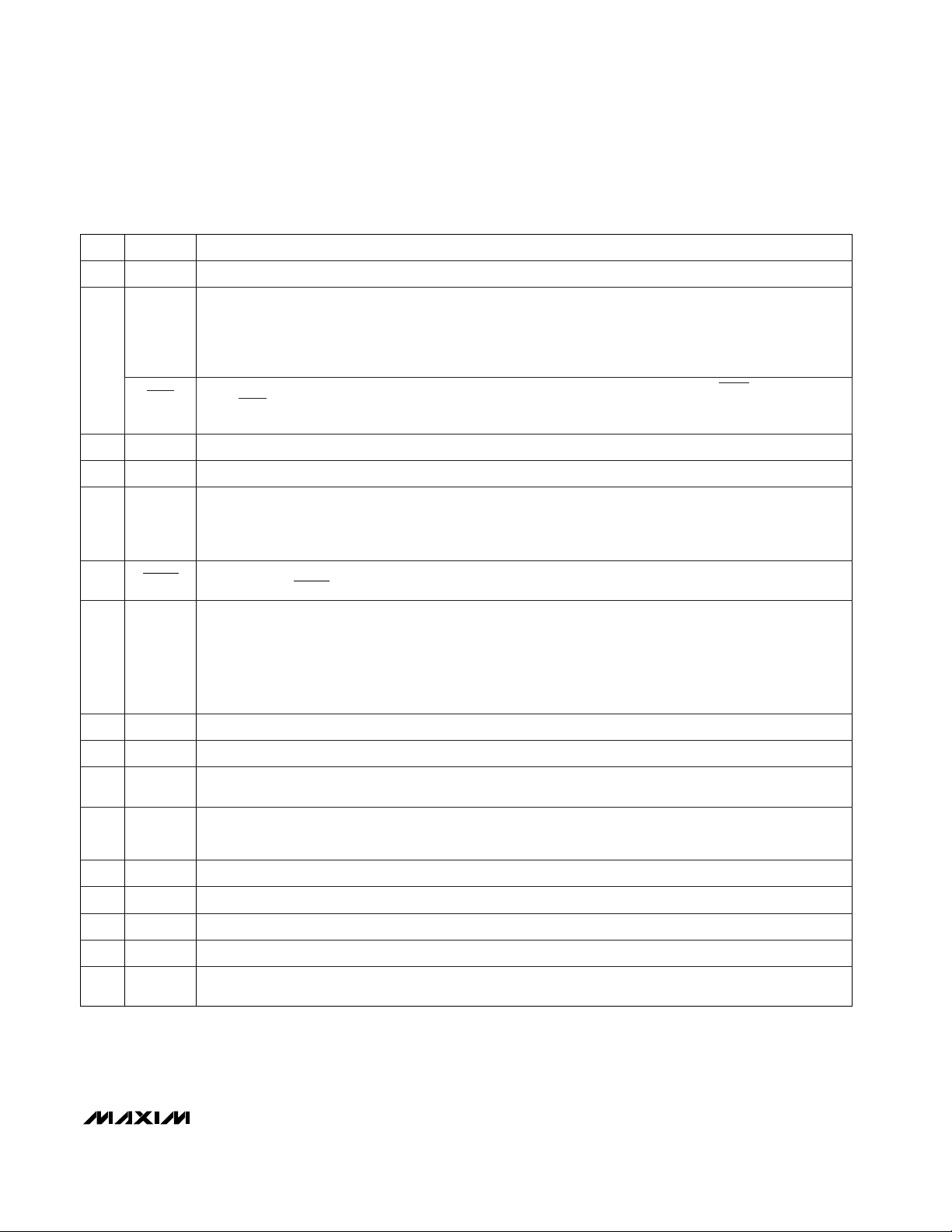
SHDN
DH
+12V
OUTPUT
+5V
OUTPUT
INPUT
6V TO 30V
BST
LX
DL
PGND
CSH
CSL
SS
REF
SYNC
GND
V+
VL
FB
SECFB
MAX796
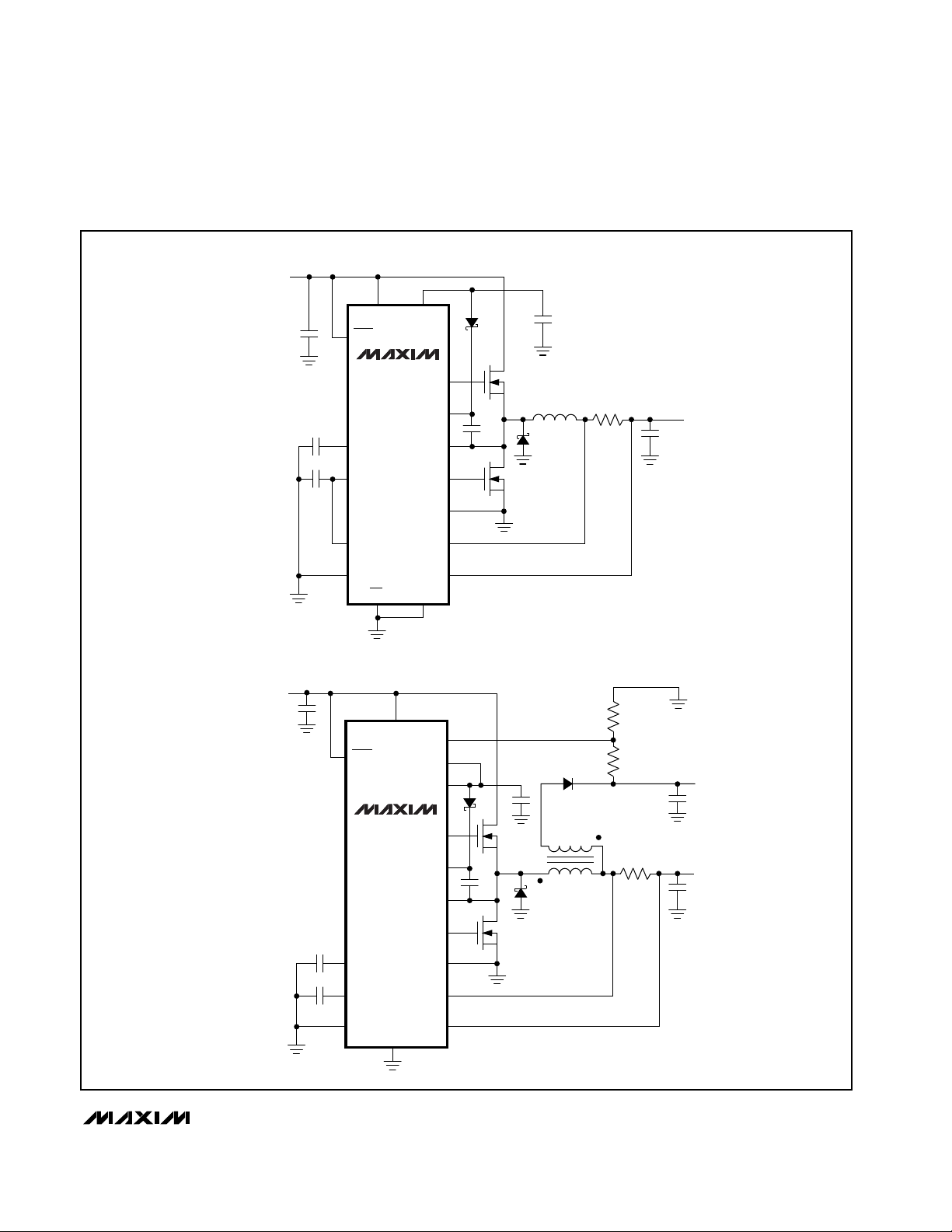
__________________________________________________Typical Operating Circuits
MAX797
SHDN
DH
+3.3V
OUTPUT
INPUT
4.5V TO 30V
BST
LX
DL
PGND
CSH
CSL
SS
REF
SYNC
GND
SKIP FB
V+ VL
Page 6
__________________________________________Typical Operating Characteristics
(TA = +25°C, unless otherwise noted.)
100
50
0.001 10.10.01 10
EFFICIENCY vs.
LOAD CURRENT, 5V/3A CIRCUIT
60
MAX796-01
LOAD CURRENT (A)
EFFICIENCY (%)
70
80
90
STANDARD MAX797 5V/3A
CIRCUIT, FIGURE 1
f = 300kHz
VIN = 6V
VIN = 30V
100
50
0.001 10.10.01 10
EFFICIENCY vs.
LOAD CURRENT, 3.3V/3A CIRCUIT
60
MAX796-02
LOAD CURRENT (A)
EFFICIENCY (%)
70
80
90
STANDARD MAX797 3.3V/3A
CIRCUIT, FIGURE 1
f = 300kHz
VIN = 12V
VIN = 30V
VIN = 5V
100
40
50
60
70
80
90
0.1 1 10
EFFICIENCY vs.
LOAD CURRENT, 3.3V/10A CIRCUIT
MAX796-03
LOAD CURRENT (A)
EFFICIENCY (%)
SKIP = LOW
SKIP = HIGH
STANDARD MAX797 3.3V/10A
CIRCUIT, FIGURE 1
f = 300kHz
V
IN
= 5V
MAX796/MAX797/MAX799
Step-Down Controllers with
Synchronous Rectifier for CPU Power
6 _______________________________________________________________________________________
MAX799
SHDN
DH
–5V
OUTPUT
+5V
OUTPUT
INPUT 6V TO 30V
BST
LX
DL
PGND
CSH
CSL
SS
REF
FROM
REF
SYNC
GND
V+
VL
FB
SECFB
_____________________________________Typical Operating Circuits (continued)
Page 7
MAX796/MAX797/MAX799
Step-Down Controllers with
Synchronous Rectifier for CPU Power
_______________________________________________________________________________________
7
____________________________Typical Operating Characteristics (continued)
(TA = +25°C, unless otherwise noted.)
0
200µ
400µ
600µ
800µ
14m
15m
16m
0 4 8 12 16 20 24 28 32
QUIESCENT SUPPLY CURRENT
vs. SUPPLY VOLTAGE,
5V/3A CIRCUIT IN IDLE MODE
MAX796-04
SUPPLY VOLTAGE (V)
SUPPLY CURRENT (A)
STANDARD MAX797 APPLICATION
CONFIGURED FOR 5V
SKIP = LOW
SYNC = REF
0
0.2
0.4
0.6
0.8
1.2
1.0
1.4
1.6
0 4 8 12 16 20 24 28 32
SHUTDOWN SUPPLY CURRENT
vs. SUPPLY VOLTAGE
MAX796-07
SUPPLY VOLTAGE (V)
SUPPLY CURRENT (µA)
DEVICE CURRENT ONLY
SHDN = LOW
0
200
400
600
800
1200
1000
1400
0 4 8 12 16 20 24 28 32
MAX796-05
SUPPLY VOLTAGE (V)
SUPPLY CURRENT (µA)
QUIESCENT SUPPLY CURRENT
vs. SUPPLY VOLTAGE,
3.3V/3A CIRCUIT IN IDLE MODE
STANDARD MAX797 3.3V/3A
CIRCUIT, FIGURE 1
SKIP = LOW
SYNC = REF
SWITCHING
NOT SWITCHING
(FB FORCED TO 3.5V)
0
10
20
30
0 4 8 12 16 20 24 28 32
MAX796-06
SUPPLY VOLTAGE (V)
SUPPLY CURRENT (mA)
QUIESCENT SUPPLY CURRENT vs.
SUPPLY VOLTAGE, LOW-NOISE MODE
f = 150kHz
f = 300kHz
STANDARD MAX797 3.3V/3A
CIRCUIT, FIGURE 1
SKIP = HIGH
0
0.01 1 100.1
DROPOUT VOLTAGE vs.
LOAD CURRENT
200
100
300
400
500
600
700
800
MAX796-08
LOAD CURRENT (A)
V
IN
- V
OUT
(mV)
STANDARD MAX797 APPLICATION
CONFIGURED FOR 5V
V
OUT
> 4.8V
f = 150kHz
f = 300kHz
0
1 100 100010
REF LOAD-REGULATION ERROR
vs. LOAD CURRENT
5
10
15
20
MAX796-09
REF LOAD CURRENT (µA)
LOAD REGULATION ∆V (mV)
0
200
100
300
400
500
0 20 40 60 80
MAX796-10
VL LOAD CURRENT (mA)
LOAD REGULATION ∆V (mV)
VL LOAD-REGULATION ERROR
vs. LOAD CURRENT
0
50
100
150
200
250
300
350
400
450
0 4 8 12 16 20 24 28 32
MAX796-11
SUPPLY VOLTAGE (V)
MAXIMUM SECONDARY CURRENT (mA)
MAX796
MAXIMUM SECONDARY CURRENT
vs. SUPPLY VOLTAGE, 5V/15V CIRCUIT
I
OUT
(MAIN) = 0A
I
OUT
(MAIN) = 3A
CIRCUIT OF FIGURE 11
TRANSFORMER = TTI5870
V
SEC
> 12.75V
1000
0.1
100µ 10m 1
SWITCHING FREQUENCY vs.
LOAD CURRENT
10
LOAD CURRENT (A)
SWITCHING FREQUENCY (kHz)
100
1m 100m
SYNC = REF (300kHz)
SKIP = LOW
+5V, VIN = 7.5V
1
+5V, VIN = 30V
+3.3V, VIN = 7.5V
Page 8
I
LOAD
= 100mA, VIN = 10V,
CIRCUIT OF FIGURE 1
IDLE-MODE WAVEFORMS
+5V OUTPUT
50mV/div
2V/div
200µs/div
I
LOAD
= 1A, VIN = 16V,
CIRCUIT OF FIGURE 1
PULSE-WIDTH-MODULATION MODE WAVEFORMS
LX VOLTAGE
10V/div
+5V OUTPUT
VOLTAGE
50mV/div
500ns/div
VIN = 15V, CIRCUIT OF FIGURE 1
+5V LOAD-TRANSIENT RESPONSE
+5V OUTPUT
50mV/div
3A
0A
LOAD CURRENT
200µs/div
MAX796/MAX797/MAX799
Step-Down Controllers with
Synchronous Rectifier for CPU Power
8 _______________________________________________________________________________________
0
150
300
450
600
900
750
1050
0 3 6 9 12 15 18 21 24
MAX796
MAXIMUM SECONDARY CURRENT vs.
SUPPLY VOLTAGE, 3.3V/5V CIRCUIT
MAX796-12
SUPPLY VOLTAGE (V)
MAXIMUM SECONDARY CURRENT (mA)
I
OUT
(MAIN) = 2A
I
OUT
(MAIN) = 0A
CIRCUIT OF FIGURE 12
TRANSFORMER = TDK 1.5:1
V
SEC
≥ 4.8V
0
100
200
300
400
600
500
700
800
0 4 8 12 16 20 24 28 32
MAX799
MAXIMUM SECONDARY CURRENT
vs. SUPPLY VOLTAGE, ±5V CIRCUIT
MAX796-13
SUPPLY VOLTAGE (V)
MAXIMUM SECONDARY CURRENT (mA)
CIRCUIT OF FIGURE 13
TRANSFORMER = TTI5926
V
SEC
≤ -5.1V
I
OUT
(MAIN) = 0A
I
OUT
(MAIN) = 1A
____________________________Typical Operating Characteristics (continued)
(TA = +25°C, unless otherwise noted.)
Page 9
MAX796/MAX797/MAX799
Step-Down Controllers with
Synchronous Rectifier for CPU Power
_______________________________________________________________________________________ 9
______________________________________________________________Pin Description
Current-Sense input, High side. Current-limit level is 100mV referred to CSL.CSH8
Current-Sense input, Low side. Also serves as the feedback input in fixed-output modes.CSL9
Battery voltage input (4.5V to 30V). Bypass V+ to PGND close to the IC with a 0.1µF capacitor. Connects to a
linear regulator that powers VL.
V+10
5V Internal linear-regulator output. VL is also the supply voltage rail for the chip. VL is switched to the output
voltage via CSL (V
CSL
> 4.5V) for automatic bootstrapping. Bypass to GND with 4.7µF. VL can
supply up to 5mA for external loads.
VL11
Power Ground.PGND12
Low-noise analog Ground and feedback reference point.GND4
Oscillator Synchronization and frequency select. Tie to GND or VL for 150kHz operation; tie to REF for
300kHz operation. A high-to-low transition begins a new cycle. Drive SYNC with 0V to 5V logic levels (see the
Electrical Characteristics
table for VIHand VILspecifications). SYNC capture range is 190kHz to 340kHz
guaranteed.
SYNC5
Shutdown control input, active low. Logic threshold is set at approximately 1V (VTHof an internal N-channel
MOSFET). Tie SHDN to V+ for automatic start-up.
SHDN6
Feedback input. Regulates at FB = REF (approximately 2.505V) in adjustable mode. FB is a Dual-Mode
TM
input that also selects the fixed output voltage settings as follows:
• Connect to GND for 3.3V operation.
• Connect to VL for 5V operation.
• Connect FB to a resistor divider for adjustable mode. FB can be driven with +5V rail-to-rail logic in order to
change the output voltage under system control.
FB7
Reference voltage output. Bypass to GND with 0.33µF minimum.REF3
PIN
Secondary winding Feedback input. Normally connected to a resistor divider from an auxiliary output.
Don’t leave SECFB unconnected.
• MAX796: SECFB regulates at VSECFB = 2.505V. Tie to VL if not used.
• MAX799: SECFB regulates at VSECFB = 0V. Tie to a negative voltage through a high-value current-limit-
ing resistor (I
MAX
= 100µA) if not used.
SECFB
(MAX796/
MAX799)
2
Soft-Start timing capacitor connection. Ramp time to full current limit is approximately 1ms/nF.SS1
FUNCTIONNAME
Low-side gate-drive output. Normally drives the synchronous-rectifier MOSFET. Swings 0V to VL.DL13
Boost capacitor connection for high-side gate drive (0.1µF). BST14
Switching node (inductor) connection. Can swing 2V below ground without hazard.LX15
High-side gate-drive output. Normally drives the main buck switch. DH is a floating driver output that swings
from LX to BST, riding on the LX switching-node voltage.
DH16
Dual Mode is a trademark of Maxim Integrated Products.
Disables pulse-skipping mode when high. Connect to GND for normal use. Don’t leave SKIP unconnected.
With SKIP
grounded, the device will
automatically
change from pulse-skipping operation to full PWM opera-
tion when the load current exceeds approximately 30% of maximum. (See Table 3.)
SKIP
(MAX797)
Page 10
MAX796/MAX797/MAX799
Step-Down Controllers with
Synchronous Rectifier for CPU Power
10 ______________________________________________________________________________________
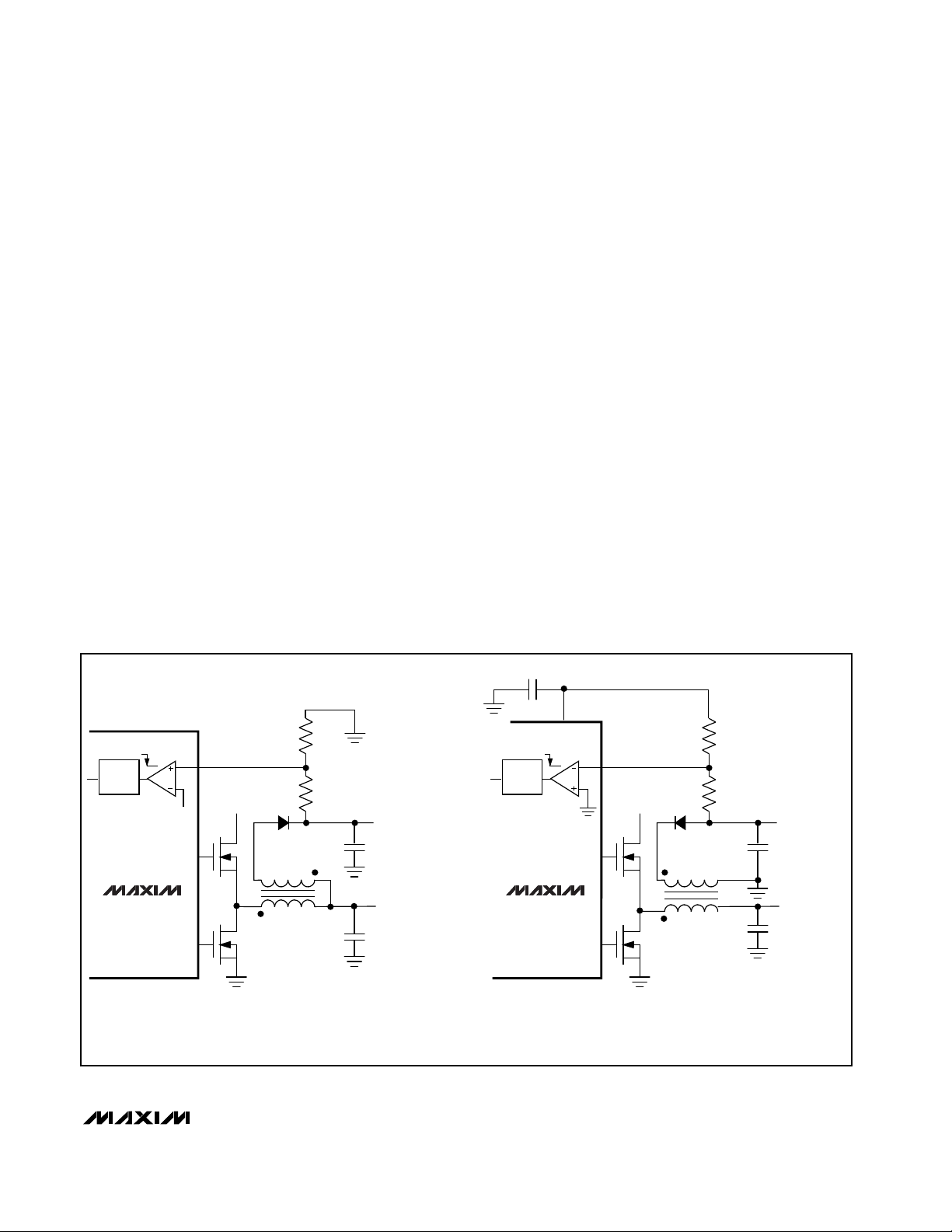
______Standard Application Circuit
It is easy to adapt the basic MAX797 single-output 3.3V
buck converter (Figure 1) to meet a wide range of
applications with inputs up to 28V (limited by choice of
external MOSFET). Simply substitute the appropriate
components from Table 1. These circuits represent a
good set of tradeoffs between cost, size, and efficiency
while staying within the worst-case specification limits
for stress-related parameters such as capacitor ripple
current. Each of these circuits is rated for a continuous
load current at TA= +85°C, as shown. The 1A, 2A and
10A applications can withstand a continuous output
short-circuit to ground. The 3A and 5A applications can
withstand a short circuit of many seconds duration, but
the synchronous-rectifier MOSFET overheats, exceeding the manufacturer’s ratings for junction temperature
by 50°C or more.
If the 3A or 5A circuit must be guaranteed to withstand
a continuous output short circuit indefinitely, see the
section
MOSFET Switches
under
Selecting Other
Components
. Don’t change the frequency of these circuits without first recalculating component values (particularly inductance value at maximum battery voltage).
_______________Detailed Description
The MAX796 is a BiCMOS, switch-mode power-supply
controller designed primarily for buck-topology regulators in battery-powered applications where high efficiency and low quiescent supply current are critical.
The MAX796 also works well in other topologies such
as boost, inverting, and CLK due to the flexibility of its
floating high-speed gate driver. Light-load efficiency is
enhanced by automatic idle-mode operation—a variable-frequency pulse-skipping mode that reduces
MAX797
CSL
CSH
VL
SYNC
FB
V+
10 11
57
14
Q1
Q2
16
15
13
D2
CMPSH-3
J1
150kHz/300kHz
JUMPER
NOTE: KEEP CURRENT-SENSE
LINES SHORT AND CLOSE
TOGETHER. SEE FIG. 10
D1
12
8
9
REF
3
GND
4
+5V AT
5mA
+3.3V
OUTPUT
GND
OUT
BST
DH
LX
DL
2
1
LOW-NOISE
CONTROL
PGND
SKIP
SS
6
ON/OFF
CONTROL
SHDN
INPUT
REF OUTPUT
+2.505V AT 100µA
C5
0.33µF
C4
4.7µF
C7
0.1µF
C6
0.01µF
(OPTIONAL)
C1
C2
C3
0.1µF
R1
L1
Figure 1. Standard 3.3V Application Circuit
Page 11

MAX796/MAX797/MAX799
Step-Down Controllers with
Synchronous Rectifier for CPU Power
______________________________________________________________________________________ 11
Table 1. Component Selection for Standard 3.3V Applications
Table 2. Component Suppliers
*
Distributor
losses due to MOSFET gate charge. The step-down
power-switching circuit consists of two N-channel
MOSFETs, a rectifier, and an LC output filter. The output voltage is the average of the AC voltage at the
switching node, which is adjusted and regulated by
changing the duty cycle of the MOSFET switches. The
gate-drive signal to the N-channel high-side MOSFET
must exceed the battery voltage and is provided by a
flying capacitor boost circuit that uses a 100nF capacitor connected to BST.
The MAX796 contains nine major circuit blocks, which
are shown in Figure 2.
[1] 714-960-6492(714) 969-2491Matsuo
[1] 512-992-3377(512) 992-7900IRC
[1] 310-322-3332(310) 322-3331International Rectifier
[1] 605-665-1627(605) 668-4131Dale
[1] 561-241-9339(561) 241-7876Coiltronics
[1] 847-639-1469(847) 639-6400Coilcraft
[1] 516-435-1824(516) 435-1110Central Semiconductor
[1] 803-626-3123(803) 946-0690AVX
FACTORY FAX
[Country Code]
USA PHONEMANUFACTURER
[1] 864-963-6521(864) 963-6300Kemet
1.5µH, 11A, 3.5mΩ
Coiltronics
CTX03-12357-1
4.7µH, 5.5A Ferrite
Coilcraft DO3316-472
10µH, 3A Ferrite
Sumida CDRH125
33µH, 2.2A Ferrite
Dale LPE6562-330MB
47µH, 1.2A Ferrite or
Kool-Mu
Sumida CD75-470
L1 Inductor
3 x 0.02Ω IRC
LR2010-01-R020
(3 in parallel)
0.015Ω IRC
LR2010-01-015
0.025Ω IRC
LR2010-01-R025
0.039Ω IRC
LR2010-01-R039
0.062Ω IRC
LR2010-01-R062
R1 Resistor
1N5820 NIEC
NSQ03A02, or
Motorola MBRS340T3
1N5821 NIEC
NSQ03A04 or
Motorola MBRS340T3
1N5819 NIEC
EC10QS03 or
Motorola MBRS130T3
1N5817 NIEC
EC10QS02L or
Motorola MBRS130T3
1N5817 Motorola
MBR0502L SOD-89
D1 Rectifier
4 x 220µF, 10V
Sanyo OS-CON
10SA220M
3 x 220µF, 10V AVX
TPS or Sprague 595D
220µF, 10V AVX TPS
or Sprague 595D
150µF, 10V AVX TPS
or Sprague 595D
150µF, 10V AVX TPS
or Sprague 595D
C2 Output
Capacitor
2 x 220µF, 10V
Sanyo OS-CON
10SA220M
4 x 22µF, 35V AVX
TPS or Sprague 595D
2 x 22µF, 35V AVX
TPS or Sprague 595D
2 x 22µF, 35V AVX
TPS or Sprague 595D
22µF, 35V AVX TPS
or Sprague 595D
C1 Input
Capacitor
Motorola
MTD75N03HDL
D2PAK
Motorola
MTD20N03HDL
DPAK
Motorola
MMSF5N03HD or
Si9410
Motorola 1/2
MMDF3N03HD or 1/2
Si9936
International Rectifier
1/2 IRF7101
Q2 Low-Side
MOSFET
Motorola
MTD75N03HDL
D2PAK
Motorola
MTD20N03HDL
DPAK
Motorola
MMSF5N03HD or
Si9410
Motorola 1/2
MMDF3N03HD or 1/2
Si9936
International Rectifier
1/2 IRF7101
Q1 High-Side
MOSFET
4.5V to 6V4.75V to 24V4.75V to 28V4.75V to 18V4.75V to 18VInput Range
{1} 847-390-4405(847) 390-4461TDK
[81] 3-3607-5144(847) 956-0666Sumida
[1] 603-224-1430(603) 224-1961Sprague
[1] 408-970-3950
(408) 988-8000
(800) 554-5565
Siliconix
[81] 7-2070-1174(619) 661-6835Sanyo
[81] 3-3494-7414(805) 867-2555*NIEC
[1] 814-238-0490
(814) 237-1431
(800) 831-9172
Murata-Erie
FACTORY FAX
[Country Code]
USA PHONEMANUFACTURER
[1] 702-831-3521(702) 831-0140Transpower Technologies[1] 602-994-6430(602) 303-5454Motorola
LOAD CURRENT
10A4A3A2A1A
COMPONENT
300kHz300kHz300kHz300kHz150kHzFrequency
Desktop 5V-to-3VHigh-End NotebookNotebookSub-NotebookPDAApplication
Page 12

MAX796/MAX797/MAX799
Step-Down Controllers with
Synchronous Rectifier for CPU Power
12 ______________________________________________________________________________________
MAX796
1V
CSL
CSH
REF
GND
4V
FB
ADJ FB
5V FB
3.3V FB
SYNC
LPF
60kHz
PWM
COMPARATOR
OUT
V+
BATTERY VOLTAGE
4.5V
VL
TO
CSL
+5V AT 5mA
BST
DH
LX
DL
PGND
SECFB
MAIN
OUTPUT
AUXILIARY
OUTPUT
SHDN
PWM
LOGIC
SHDN
SS
ON/OFF
+2.505V
AT 100µA
+5V LINEAR
REGULATOR
+2.505V
REF
Figure 2. MAX796 Block Diagram
Page 13

MAX796/MAX797/MAX799
Step-Down Controllers with
Synchronous Rectifier for CPU Power
______________________________________________________________________________________ 13
PWM Controller Blocks:
• Multi-Input PWM Comparator
• Current-Sense Circuit
• PWM Logic Block
• Dual-Mode Internal Feedback Mux
• Gate-Driver Outputs
• Secondary Feedback Comparator
Bias Generator Blocks:
• +5V Linear Regulator
• Automatic Bootstrap Switchover Circuit
• +2.505V Reference
These internal IC blocks aren’t powered directly from
the battery. Instead, a +5V linear regulator steps down
the battery voltage to supply both the IC internal rail (VL
pin) as well as the gate drivers. The synchronousswitch gate driver is directly powered from +5V VL,
while the high-side-switch gate driver is indirectly powered from VL via an external diode-capacitor boost circuit. An automatic bootstrap circuit turns off the +5V
linear regulator and powers the IC from its output voltage if the output is above 4.5V.
PWM Controller Block
The heart of the current-mode PWM controller is a
multi-input open-loop comparator that sums three signals: output voltage error signal with respect to the reference voltage, current-sense signal, and slope
compensation ramp (Figure 3). The PWM controller is a
direct summing type, lacking a traditional error amplifier and the phase shift associated with it. This directsumming configuration approaches the ideal of
cycle-by-cycle control over the output voltage.
Under heavy loads, the controller operates in full PWM
mode. Each pulse from the oscillator sets the main
PWM latch that turns on the high-side switch for a period determined by the duty factor (approximately
V
OUT/VIN
). As the high-switch turns off, the synchronous rectifier latch is set. 60ns later the low-side switch
turns on, and stays on until the beginning of the next
clock cycle (in continuous mode) or until the inductor
current crosses zero (in discontinuous mode). Under
fault conditions where the inductor current exceeds the
100mV current-limit threshold, the high-side latch
resets and the high-side switch turns off.
At light loads (SKIP = low), the inductor current fails to
exceed the 30mV threshold set by the minimum-current
comparator. When this occurs, the controller goes into
idle mode, skipping most of the oscillator pulses in
order to reduce the switching frequency and cut back
gate-charge losses. The oscillator is effectively gated
off at light loads because the minimum-current comparator immediately resets the high-side latch at the
beginning of each cycle, unless the feedback signal
falls below the reference voltage level.
When in PWM mode, the controller operates as a fixedfrequency current-mode controller where the duty ratio
is set by the input/output voltage ratio. The currentmode feedback system regulates the peak inductor
current as a function of the output voltage error signal.
Since the average inductor current is nearly the same
as the peak current, the circuit acts as a switch-mode
transconductance amplifier and pushes the second
output LC filter pole, normally found in a duty-factorcontrolled (voltage-mode) PWM, to a higher frequency.
To preserve inner-loop stability and eliminate regenerative inductor current “staircasing,” a slope-compensation ramp is summed into the main PWM comparator to
reduce the apparent duty factor to less than 50%.
The relative gains of the voltage- and current-sense
inputs are weighted by the values of current sources
that bias three differential input stages in the main PWM
comparator (Figure 4). The relative gain of the voltage
comparator to the current comparator is internally fixed
at K = 2:1. The resulting loop gain (which is relatively
low) determines the 2.5% typical load regulation error.
The low loop-gain value helps reduce output filter
capacitor size and cost by shifting the unity-gain
crossover to a lower frequency.
SHDN SKIP
LOAD
CURRENT
MODE
NAME
DESCRIPTION
Low X X Shutdown
All circuit blocks
turned off; supply
current = 1µA typ
High Low
Low,
<10%
Idle
Pulse-skipping;
supply current =
700µA typ at VIN=
10V; discontinuous
inductor current
High Low
Medium,
<30%
Idle
Pulse-skipping;
continuous inductor
current
High Low
High,
>30%
PWM
Constant-frequency
PWM; continuous
inductor current
High High X
Low Noise*
(PWM)
Constant-frequency
PWM regardless of
load; continuous
inductor current
even at no load
Table 3. Operating-Mode Truth Table
* MAX796/MAX799 have no SKIP pin and therefore can’t go
into low-noise mode.
X = Don’t Care
Page 14

MAX796/MAX797/MAX799
Step-Down Controllers with
Synchronous Rectifier for CPU Power
14 ______________________________________________________________________________________
SHOOTTHROUGH
CONTROL
R
Q
30mV
R
Q
LEVEL
SHIFT
1µs
SINGLE-SHOT
1X
MAIN PWM
COMPARATOR
OSC
LEVEL
SHIFT
CURRENT
LIMIT
VL
24R
1R
2.5V
4µA
SYNCHRONOUS
RECTIFIER CONTROL
REF
SS
SHDN
–100mV
NOTE 1
CSH
CSL
FROM
FEEDBACK
DIVIDER
BST
DH
LX
VL
DL
PGND
S
S
SLOPE COMP
N
SKIP
(MAX797
ONLY)
REF (MAX796)
GND (MAX799)
MAX796, MAX799 ONLY
SECFB
NOTE 1: COMPARATOR INPUT POLARITIES
ARE REVERSED FOR THE MAX799.
Figure 3. PWM Controller Detailed Block Diagram
Page 15

MAX796/MAX797/MAX799
Step-Down Controllers with
Synchronous Rectifier for CPU Power
______________________________________________________________________________________ 15
The output filter capacitor C2 sets a dominant pole in
the feedback loop. This pole must roll off the loop gain
to unity before the zero introduced by the output
capacitor’s parasitic resistance (ESR) is encountered
(see
Design Procedure
section). A 60kHz pole-zero
cancellation filter provides additional rolloff above the
unity-gain crossover. This internal 60kHz lowpass compensation filter cancels the zero due to the filter capacitor’s ESR. The 60kHz filter is included in the loop in
both fixed- and adjustable-output modes.
Synchronous-Rectifier Driver (DL Pin)
Synchronous rectification reduces conduction losses in
the rectifier by shunting the normal Schottky diode with
a low-resistance MOSFET switch. The synchronous rectifier also ensures proper start-up of the boost-gate driver circuit. If you must omit the synchronous power
MOSFET for cost or other reasons, replace it with a
small-signal MOSFET such as a 2N7002.
If the circuit is operating in continuous-conduction
mode, the DL drive waveform is simply the complement
of the DH high-side drive waveform (with controlled
dead time to prevent cross-conduction or “shootthrough”). In discontinuous (light-load) mode, the synchronous switch is turned off as the inductor current
falls through zero. The synchronous rectifier works
under all operating conditions, including idle mode.
The synchronous-switch timing is further controlled by
the secondary feedback (SECFB) signal in order to
improve multiple-output cross-regulation (see
Secondary Feedback-Regulation Loop
section).
Internal VL and REF Supplies
An internal regulator produces the 5V supply (VL) that
powers the PWM controller, logic, reference, and other
blocks within the MAX796. This +5V low-dropout linear
regulator can supply up to 5mA for external loads, with
a reserve of 20mA for gate-drive power. Bypass VL to
GND with 4.7µF. Important: VL must not be allowed to
exceed 6V. Measure VL with the main output fully
loaded. If VL is being pumped up above 5.5V, the
probable cause is either excessive boost-diode capacitance or excessive ripple at V+. Use only small-signal
diodes for D2 (1N4148 preferred) and bypass V+ to
PGND with 0.1µF directly at the package pins.
The 2.505V reference (REF) is accurate to ±1.6% over
temperature, making REF useful as a precision system
reference. Bypass REF to GND with 0.33µF minimum.
REF can supply up to 1mA for external loads. However,
if tight-accuracy specs for either VOUT or REF are
essential, avoid loading REF with more than 100µA.
Loading REF reduces the main output voltage slightly,
according to the reference-voltage load regulation
error. In MAX799 applications, ensure that the SECFB
divider doesn’t load REF heavily.
When the main output voltage is above 4.5V, an internal Pchannel MOSFET switch connects CSL to VL while simultaneously shutting down the VL linear regulator. This
action bootstraps the IC, powering the internal circuitry
from the output voltage, rather than through a linear regulator from the battery. Bootstrapping reduces power dissipation caused by gate-charge and quiescent losses by
providing that power from a 90%-efficient switch-mode
source, rather than from a 50%-efficient linear regulator.
FB
REF
CSH
CSL
SLOPE COMPENSATION
VL
I1
R1 R2
TO PWM
LOGIC
OUTPUT DRIVER
UNCOMPENSATED
HIGH-SPEED
LEVEL TRANSLATOR
AND BUFFER
I2 I3
Figure 4. Main PWM Comparator Block Diagram
Page 16

MAX796/MAX797/MAX799
Step-Down Controllers with
Synchronous Rectifier for CPU Power
16 ______________________________________________________________________________________
It’s often possible to achieve a bootstrap-like effect, even
for circuits that are set to V
OUT
< 4.5V, by powering VL
from an external-system +5V supply. To achieve this
pseudo-bootstrap, add a Schottky diode between the
external +5V source and VL, with the cathode to the VL
side. This circuit provides a 1% to 2% efficiency boost
and also extends the minimum battery input to less than
4V. The external source must be in the range of 4.8V to
6V. Another way to achieve a pseudo-bootstrap is to add
an extra flyback winding to the main inductor to generate
the +5V bootstrap source, as shown in the +3.3V/+5V
Dual-Output Application (Figure 12).
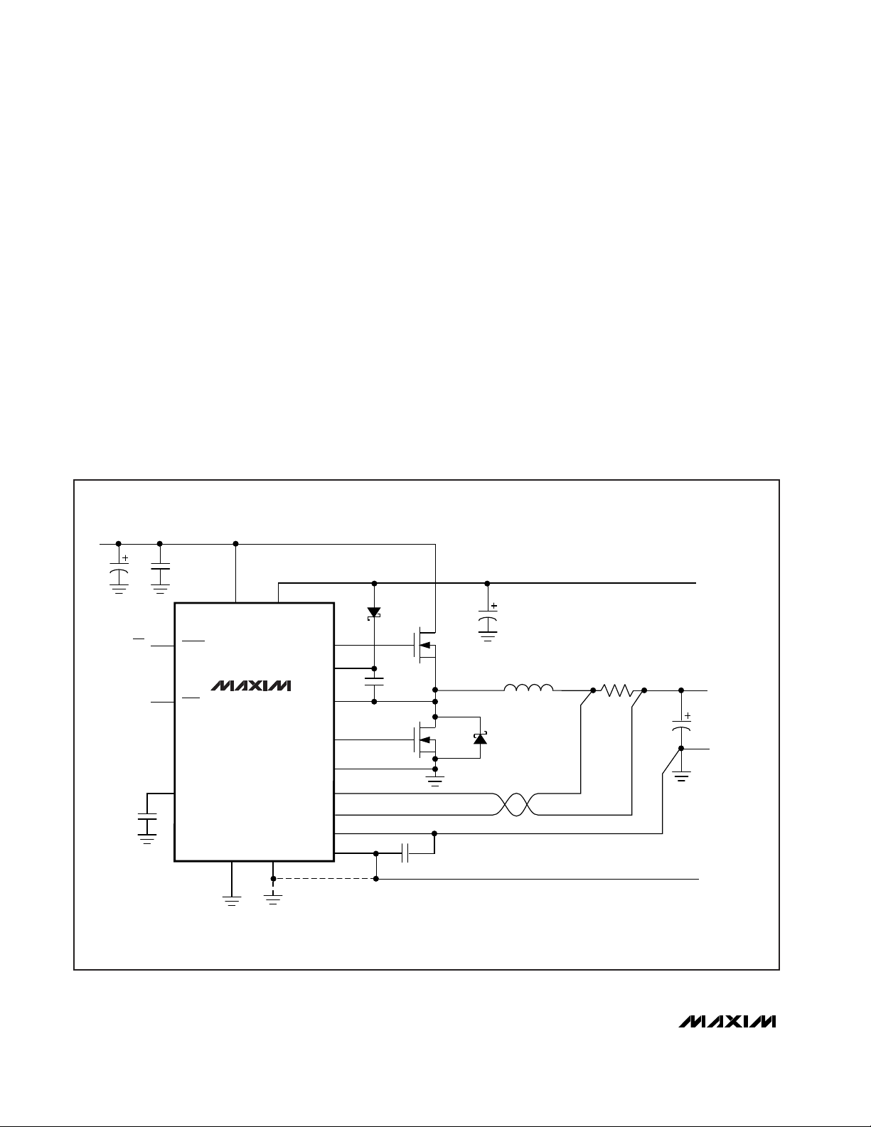
Boost High-Side
Gate-Driver Supply (BST Pin)
Gate-drive voltage for the high-side N-channel switch is
generated by a flying-capacitor boost circuit as shown
in Figure 5. The capacitor is alternately charged from
the VL supply and placed in parallel with the high-side
MOSFET’s gate-source terminals.
On start-up, the synchronous rectifier (low-side MOSFET) forces LX to 0V and charges the BST capacitor to
5V. On the second half-cycle, the PWM turns on the
high-side MOSFET by closing an internal switch
between BST and DH. This provides the necessary
enhancement voltage to turn on the high-side switch,
an action that “boosts” the 5V gate-drive signal above
the battery voltage.
Ringing seen at the high-side MOSFET gate (DH) in
discontinuous-conduction mode (light loads) is a natural operating condition, and is caused by the residual
energy in the tank circuit formed by the inductor and
stray capacitance at the switching node LX. The gatedriver negative rail is referred to LX, so any ringing
there is directly coupled to the gate-drive output.
Current-Limiting and
Current-Sense Inputs (CSH and CSL)
The current-limit circuit resets the main PWM latch and
turns off the high-side MOSFET switch whenever the
voltage difference between CSH and CSL exceeds
100mV. This limiting is effective for both current flow
directions, putting the threshold limit at ±100mV. The
tolerance on the positive current limit is ±20%, so the
external low-value sense resistor must be sized for
80mV/R1 to guarantee enough load capability, while
components must be designed to withstand continuous
current stresses of 120mV/R1.
For breadboarding purposes or very high-current applications, it may be useful to wire the current-sense inputs
with a twisted pair rather than PC traces. This twisted
pair needn’t be anything special, perhaps two pieces of
wire-wrap wire twisted together.
Oscillator Frequency and
Synchronization (SYNC Pin)
The SYNC input controls the oscillator frequency.
Connecting SYNC to GND or to VL selects 150kHz
operation; connecting SYNC to REF selects 300kHz.
SYNC can also be used to synchronize with an external
5V CMOS or TTL clock generator. SYNC has a guaranteed 190kHz to 340kHz capture range.
300kHz operation optimizes the application circuit for
component size and cost. 150kHz operation provides
increased efficiency and improved load-transient
response at low input-output voltage differences (see
Low-Voltage Operation
section).
Low-Noise Mode (SKIP Pin)
The low-noise mode (SKIP = high) is useful for minimizing RF and audio interference in noise-sensitive applications such as Soundblaster™ hi-fi audio-equipped
systems, cellular phones, RF communicating computers, and electromagnetic pen-entry systems. See the
summary of operating modes in Table 3. SKIP can be
driven from an external logic signal.
The MAX797 can reduce interference due to switching
noise by ensuring a constant switching frequency
regardless of load and line conditions, thus concentrating the emissions at a known frequency outside the
system audio or IF bands. Choose an oscillator fre-
MAX796
MAX797
MAX799
BST
VL
+5V
VL SUPPLY
BATTERY
INPUT
VL
VL
DH
LX
DL
PWM
LEVEL
TRANSLATOR
Figure 5. Boost Supply for Gate Drivers
Soundblaster is a trademark of Creative Labs.
Page 17

MAX796/MAX797/MAX799
Step-Down Controllers with
Synchronous Rectifier for CPU Power
______________________________________________________________________________________ 17
quency where harmonics of the switching frequency
don’t overlap a sensitive frequency band. If necessary,
synchronize the oscillator to a tight-tolerance external
clock generator.
The low-noise mode (SKIP = high) forces two changes
upon the PWM controller. First, it ensures fixed-frequency operation by disabling the minimum-current comparator and ensuring that the PWM latch is set at the
beginning of each cycle, even if the output is in regulation. Second, it ensures continuous inductor current
flow, and thereby suppresses discontinuous-mode
inductor ringing by changing the reverse current-limit
detection threshold from zero to -100mV, allowing the
inductor current to reverse at very light loads.
In most applications, SKIP should be tied to GND in
order to minimize quiescent supply current. Supply current with SKIP high is typically 10mA to 20mA, depending on external MOSFET gate capacitance and
switching losses.
Forced continuous conduction via SKIP can improve
cross regulation of transformer-coupled multiple-output
supplies. This second function of the SKIP pin produces a result that is similar to the method of adding
secondary regulation via the SECFB feedback pin, but
with much higher quiescent supply current. Still,
improving cross regulation by enabling SKIP instead of
building in SECFB feedback can be useful in noisesensitive applications, since SECFB and SKIP are
mutually exclusive pins/functions in the MAX796 family.
Adjustable-Output Feedback
(Dual-Mode FB Pin)
Adjusting the main output voltage with external resistors is easy for any of the devices in the MAX796 family,
via the circuit of Figure 6. The nominal output voltage
(given by the formula in Figure 6) should be set approximately 2% high in order to make up for the MAX796’s
-2.5% typical load-regulation error. For example, if
designing for a 3.0V output, use a resistor ratio that
results in a nominal output voltage of 3.06V. This slight
offsetting gives the best possible accuracy.
Recommended normal values for R5 range from 5kΩ to
100kΩ. To achieve a 2.505V nominal output, simply
connect FB to CSL directly. To achieve output voltages
lower than 2.5V, use an external reference-voltage
source higher than V
REF
, as shown in Figure 7. For best
accuracy, this second reference voltage should be
much higher than V
REF
. Alternatively, an external op
amp could be used to gain-up REF in order to create
the second reference source. This scheme requires a
minimum load on the output in order to sink the R3/R4
divider current.
Remote sensing of the output voltage, while not possible in fixed-output mode due to the combined nature of
the voltage- and current-sense input (CSL), is easy to
achieve in adjustable mode by using the top of the
external resistor divider as the remote sense point.
Fixed-output accuracy is guaranteed to be ±4% over
all conditions. In special circumstances, it may be necessary to improve upon this output accuracy. The HighAccuracy Adjustable-Output Application (Figure 18)
provides ±2.5% accuracy by adding an integrator-type
error amplifier.
The breakdown voltage rating of the current-sense
inputs (7V absolute maximum) determines the 6V maximum output adjustment range. To extend this output
range, add two matched resistor dividers and speedup capacitors to form a level translator, as shown in
Figure 8. Be sure to set these resistor ratios accurately
(using 0.1% resistors), to avoid adding excessive error
to the 100mV current-limit threshold.
Secondary Feedback-Regulation Loop
(SECFB Pin)
A flyback winding control loop regulates a secondary
winding output (MAX796/MAX799 only), improving
cross-regulation when the primary is lightly loaded or
when there is a low input-output differential voltage. If
SECFB crosses its regulation threshold (VREF for the
MAX796
MAX797
MAX799
CSL
CSH
GND
FB
R4
R5
MAIN
OUTPUT
REMOTE
SENSE
LINES
DH
DL
V
OUT
WHERE V
REF
(NOMINAL) = 2.505V
= V
REF
(1 + –––)
R4
R5
V+
Figure 6. Adjusting the Main Output Voltage
Page 18

MAX796/MAX797/MAX799
Step-Down Controllers with
Synchronous Rectifier for CPU Power
18 ______________________________________________________________________________________
MAX796), a 1µs one-shot is triggered that extends the
low-side switch’s on-time beyond the point where the
inductor current crosses zero (in discontinuous mode).
This causes the inductor (primary) current to reverse,
which in turn pulls current out of the output filter capacitor
and causes the flyback transformer to operate in the forward mode. The low impedance presented by the transformer secondary in the forward mode dumps current into
the secondary output, charging up the secondary capacitor and bringing SECFB back into regulation. The SECFB
feedback loop does not improve secondary output accuracy in normal flyback mode, where the main (primary)
output is heavily loaded. In this mode, secondary output
accuracy is determined, as usual, by the secondary rectifier drop, turns ratio, and accuracy of the main output
voltage. So, a linear post-regulator may still be needed in
order to meet tight output accuracy specifications.
The secondary output voltage-regulation point is determined by an external resistor divider at SECFB. For negative output voltages, the SECFB comparator is referenced
to GND (MAX799); for positive output voltages, SECFB
regulates at the 2.505V reference (MAX796). As a result,
output resistor divider connections and design equations
for the two device types differ slightly (Figure 9).
Ordinarily, the secondary regulation point is set 5% to
10% below the voltage normally produced by the flyback
effect. For example, if the output voltage as determined
by the turns ratio is +15V, the feedback resistor ratio
should be set to produce about +13.5V; otherwise, the
SECFB one-shot might be triggered unintentionally, causing an unnecessary increase in supply current and output
noise. In negative-output (MAX799) applications, the
resistor divider acts as a load on the internal reference,
which in turn can cause errors at the main output. Avoid
overloading REF (see the Reference Load-Regulation
Error vs. Load Current graph in the
Typical Operating
Characteristics
). 100kΩ is a good value for R3 in MAX799
circuits.
Soft-Start Circuit (SS)
Soft-start allows a gradual increase of the internal current-limit level at start-up for the purpose of reducing
input surge currents, and perhaps for power-supply
sequencing. In shutdown mode, the soft-start circuit
holds the SS capacitor discharged to ground. When
SHDN goes high, a 4µA current source charges the SS
capacitor up to 3.2V. The resulting linear ramp waveform causes the internal current-limit level to increase
proportionally from 20mV to 100mV. The main output
capacitor thus charges up relatively slowly, depending
on the SS capacitor value. The exact time of the output
rise depends on output capacitance and load current
and is typically 1ms per nanofarad of soft-start capacitance. With no SS capacitor connected, maximum current limit is reached within 10µs.
Shutdown
Shutdown mode (SHDN = 0V) reduces the V+ supply
current to typically 1µA. In this mode, the reference and
VL are inactive. SHDN is a logic-level input, but it can
be safely driven to the full V+ range. Connect SHDN to
V+ for automatic start-up. Do not allow slow transitions
(slower than 0.02V/µs) on SHDN.
MAX796
MAX797
MAX799
MAX874
CSL
CSH
GND
FB
R5
VREF2 >>VREF
(4.096V)
R4
MAIN
OUTPUT
DH
DL
V
OUT
= V
REF
- (V
REF2
- V
REF
)
(–––)
R4
R5
V+
Figure 7. Output Voltage Less than 2.5V
MAX796
MAX797
MAX799
CSL
CSH
0.01µF
0.01µF
GND
FB
OUTPUT
(8V AS
SHOWN)
DH
DL
V
OUT
R
SENSE
DIVIDER IMPEDANCE ≤ 5kΩ
(EACH LEG)
= V
REF
(1 + –––)
R3
R4
V+
R1
2.43k
R2
1.1k
R3
2.43k
R4
1.1k
Figure 8. Adjusting the Output Voltage to Greater than 6V
Page 19
MAX796/MAX797/MAX799
Step-Down Controllers with
Synchronous Rectifier for CPU Power
______________________________________________________________________________________ 19
_________________Design Procedure
The five pre-designed standard application circuits
(Figure 1 and Table 1) contain ready-to-use solutions
for common applications. Use the following design procedure to optimize the basic schematic for different
voltage or current requirements. Before beginning a
design, firmly establish the following:
V
IN(MAX)
, the maximum input (battery) voltage. This
value should include the worst-case conditions, such
as no-load operation when a battery charger or AC
adapter is connected but no battery is installed.
V
IN(MAX)
must not exceed 30V. This 30V upper limit is
determined by the breakdown voltage of the BST floating gate driver to GND (36V absolute maximum).
V
IN(MIN)
, the minimum input (battery) voltage. This
should be taken at full-load under the lowest battery
conditions. If V
IN(MIN)
is less than 4.5V, a special circuit
must be used to externally hold up VL above 4.8V. If
the minimum input-output difference is less than 1.5V,
the filter capacitance required to maintain good AC
load regulation increases.
Inductor Value
The exact inductor value isn’t critical and can be
adjusted freely in order to make tradeoffs among size,
cost, and efficiency. Although lower inductor values will
minimize size and cost, they will also reduce efficiency
due to higher peak currents. To permit use of the physically smallest inductor, lower the inductance until the
circuit is operating at the border between continuous
and discontinuous modes. Reducing the inductor value
even further, below this crossover point, results in discontinuous-conduction operation even at full load. This
helps reduce output filter capacitance requirements but
causes the core energy storage requirements to
increase again. On the other hand, higher inductor values will increase efficiency, but at some point resistive
losses due to extra turns of wire will exceed the benefit
gained from lower AC current levels. Also, high inductor values can affect load-transient response; see the
V
SAG
equation in the
Low-Voltage Operation
section.
The following equations are given for continuous-conduction operation since the MAX796 is mainly intended
for high-efficiency battery-powered applications. See
Appendix A in Maxim’s
Battery Management and DC-
DC Converter Circuit Collection
for crossover point and
discontinuous-mode equations. Discontinuous conduction doesn’t affect normal idle-mode operation.
MAX799
NEGATIVE
SECONDARY
OUTPUT
MAIN
OUTPUT
DH
V+
SECFB
R3
R2
1-SHOT
TRIG
DL
0.33µF
REF
MAX796
POSITIVE
SECONDARY
OUTPUT
MAIN
OUTPUT
DH
V+
SECFB
2.505V REF
R3
R2
1-SHOT
TRIG
DL
+V
TRIP
WHERE V
REF
(NOMINAL) = 2.505V= V
REF
(1 + –––)
R2
R3
-V
TRIP
R3 = 100kΩ (RECOMMENDED)= -V
REF
(–––)
R2
R3
Figure 9. Secondary-Output Feedback Dividers, MAX796 vs. MAX799
Page 20

MAX796/MAX797/MAX799
Step-Down Controllers with
Synchronous Rectifier for CPU Power
20 ______________________________________________________________________________________
Three key inductor parameters must be specified:
inductance value (L), peak current (I
PEAK
), and DC
resistance (RDC). The following equation includes a
constant LIR, which is the ratio of inductor peak-topeak AC current to DC load current. A higher value of
LIR allows smaller inductance, but results in higher
losses and ripple. A good compromise between size
and losses is found at a 30% ripple current to load current ratio (LIR = 0.3), which corresponds to a peak
inductor current 1.15 times higher than the DC load
current.
V
OUT(VIN(MAX)
- V
OUT
)
L = ———————————
V
IN(MAX)
x f x I
OUT
x LIR
where: f = switching frequency, normally 150kHz or
300kHz
I
OUT
= maximum DC load current
LIR = ratio of AC to DC inductor current,
typically 0.3
The peak inductor current at full load is 1.15 x I
OUT
if
the above equation is used; otherwise, the peak current
can be calculated by:
V
OUT(VIN(MAX)
- V
OUT
)
I
PEAK
= I
LOAD
+ ———————————
2 x f x L x V
IN(MAX)
The inductor’s DC resistance is a key parameter for efficiency performance and must be ruthlessly minimized,
preferably to less than 25mΩ at I
OUT
= 3A. If a standard off-the-shelf inductor is not available, choose a
core with an LI2rating greater than L x I
PEAK
2
and wind
it with the largest diameter wire that fits the winding
area. For 300kHz applications, ferrite core material is
strongly preferred; for 150kHz applications, Kool-mu
(aluminum alloy) and even powdered iron can be
acceptable. If light-load efficiency is unimportant (in
desktop 5V-to-3V applications, for example) then lowpermeability iron-powder cores, such as the
Micrometals type found in Pulse Engineering’s 2.1µH
PE-53680, may be acceptable even at 300kHz. For
high-current applications, shielded core geometries
(such as toroidal or pot core) help keep noise, EMI, and
switching-waveform jitter low.
Current-Sense Resistor Value
The current-sense resistor value is calculated according to the worst-case-low current-limit threshold voltage
(from the
Electrical Characteristics
table) and the peak
inductor current. The continuous-mode peak inductorcurrent calculations that follow are also useful for sizing
the switches and specifying the inductor-current saturation ratings. In order to simplify the calculation, I
LOAD
may be used in place of I
PEAK
if the inductor value has
been set for LIR = 0.3 or less (high inductor values)
and 300kHz operation is selected. Low-inductance
resistors, such as surface-mount metal-film resistors,
are preferred.
80mV
R
SENSE
= ————
I
PEAK
Input Capacitor Value
Place a small ceramic capacitor (0.1µF) between V+
and GND, close to the device. Also, connect a low-ESR
bulk capacitor directly to the drain of the high-side
MOSFET. Select the bulk input filter capacitor according to input ripple-current requirements and voltage rating, rather than capacitor value. Electrolytic capacitors
that have low enough ESR to meet the ripple-current
requirement invariably have more than adequate
capacitance values. Aluminum-electrolytic capacitors
such as Sanyo OS-CON or Nichicon PL are preferred
over tantalum types, which could cause power-up
surge-current failure, especially when connecting to
robust AC adapters or low-impedance batteries. RMS
input ripple current is determined by the input voltage
and load current, with the worst possible case occurring at VIN= 2 x V
OUT
:
————————
√V
OUT(VIN
- V
OUT
)
I
RMS
= I
LOAD
x ——————————
V
IN
I
RMS
= I
LOAD
/ 2 when VINis 2 x V
OUT
Output Filter Capacitor Value
The output filter capacitor values are generally determined by the ESR (effective series resistance) and voltage rating requirements rather than actual capacitance
requirements for loop stability. In other words, the lowESR electrolytic capacitor that meets the ESR requirement usually has more output capacitance than is
required for AC stability. Use only specialized low-ESR
capacitors intended for switching-regulator applications,
such as AVX TPS, Sprague 595D, Sanyo OS-CON, or
Nichicon PL series. To ensure stability, the capacitor
must meet
both
minimum capacitance and maximum
ESR values as given in the following equations:
V
REF
(1 + V
OUT
/ V
IN(MIN)
)
CF> ––––––––––––––––———–––
V
OUT
x R
SENSE
x f
R
SENSE
x V
OUT
R
ESR
< ————————
V
REF
(can be multiplied by 1.5, see note below)
Page 21

MAX796/MAX797/MAX799
Step-Down Controllers with
Synchronous Rectifier for CPU Power
______________________________________________________________________________________ 21
These equations are “worst-case” with 45 degrees of
phase margin to ensure jitter-free fixed-frequency operation and provide a nicely damped output response for
zero to full-load step changes. Some cost-conscious
designers may wish to bend these rules by using less
expensive (lower quality) capacitors, particularly if the
load lacks large step changes. This practice is tolerable,
provided that some bench testing over temperature is
done to verify acceptable noise and transient response.
There is no well-defined boundary between stable and
unstable operation. As phase margin is reduced, the
first symptom is a bit of timing jitter, which shows up as
blurred edges in the switching waveforms where the
scope won’t quite sync up. Technically speaking, this
(usually) harmless jitter is unstable operation, since the
switching frequency is now non-constant. As the
capacitor quality is reduced, the jitter becomes more
pronounced and the load-transient output voltage
waveform starts looking ragged at the edges.
Eventually, the load-transient waveform has enough
ringing on it that the peak noise levels exceed the
allowable output voltage tolerance. Note that even with
zero phase margin and gross instability present, the
output voltage noise never gets much worse than I
PEAK
x R
ESR
(under constant loads, at least).
Designers of RF communicators or other noise-sensitive analog equipment should be conservative and
stick to the guidelines. Designers of notebook computers and similar commercial-temperature-range digital
systems can multiply the R
ESR
value by a factor of 1.5
without hurting stability or transient response.
The output voltage ripple is usually dominated by the
ESR of the filter capacitor and can be approximated as
I
RIPPLE
x R
ESR
. There is also a capacitive term, so the
full equation for ripple in the continuous mode is
V
NOISE(p-p)
= I
RIPPLE
x (R
ESR
+ 1 / (2 x pi x f x CF)). In
idle mode, the inductor current becomes discontinuous
with high peaks and widely spaced pulses, so the
noise can actually be higher at light load compared to
full load. In idle mode, the output ripple can be calculated as:
0.02 x R
ESR
V
NOISE(p-p)
= —————— +
R
SENSE
0.0003 x L x [1 / V
OUT
+ 1 / (VIN- V
OUT
)]
———————————————————
(R
SENSE
)2x C
F
Transformer Design
(MAX796/MAX799 Only)
Buck-plus-flyback applications, sometimes called “coupled-inductor” topologies, need a transformer in order to
generate multiple output voltages. The basic electrical
design is a simple task of calculating turns ratios and
adding the power delivered to the secondary in order to
calculate the current-sense resistor and primary inductance. However, extremes of low input-output differentials, widely different output loading levels, and high turns
ratios can complicate the design due to parasitic transformer parameters such as inter-winding capacitance,
secondary resistance, and leakage inductance. For
examples of what is possible with real-world transformers,
see the graphs of Maximum Secondary Current vs. Input
Voltage in the
Typical Operating Characteristics.
Power from the main and secondary outputs is lumped
together to obtain an equivalent current referred to the
main output voltage (see Inductor L1 for definitions of
parameters). Set the value of the current-sense resistor
at 80mV / I
TOTAL
.
P
TOTAL
= the sum of the output power from all outputs
I
TOTAL
= P
TOTAL
/ V
OUT
= the equivalent output cur-
rent referred to V
OUT
V
OUT(VIN(MAX)
- V
OUT
)
L(primary) = —————————————
V
IN(MAX)
x f x I
TOTAL
x LIR
V
SEC
+ V
FWD
Turns Ratio N = ——————————————
V
OUT(MIN)
+ V
RECT
+ V
SENSE
where: V
SEC
is the minimum required rectified secondary-output voltage
V
FWD
is the forward drop across the secondary
rectifier
V
OUT(MIN)
is the
minimum
value of the main
output voltage (from the
Electrical
Characteristics
)
V
RECT
is the on-state voltage drop across the
synchronous-rectifier MOSFET
V
SENSE
is the voltage drop across the sense
resistor
In positive-output (MAX796) applications, the transformer secondary return is often referred to the main
output voltage rather than to ground in order to reduce
the needed turns ratio. In this case, the main output
voltage must first be subtracted from the secondary
voltage to obtain V
SEC
.
Page 22

MAX796/MAX797/MAX799
Step-Down Controllers with
Synchronous Rectifier for CPU Power
22 ______________________________________________________________________________________
______Selecting Other Components
MOSFET Switches
The two high-current N-channel MOSFETs must be
logic-level types with guaranteed on-resistance specifications at VGS= 4.5V. Lower gate threshold specs are
better (i.e., 2V max rather than 3V max). Drain-source
breakdown voltage ratings must at least equal the maximum input voltage, preferably with a 20% derating factor. The best MOSFETs will have the lowest
on-resistance per nanocoulomb of gate charge.
Multiplying R
DS(ON)
x QGprovides a meaningful figure
by which to compare various MOSFETs. Newer MOSFET process technologies with dense cell structures
generally give the best performance. The internal gate
drivers can tolerate >100nC total gate charge, but
70nC is a more practical upper limit to maintain best
switching times.
In high-current applications, MOSFET package power
dissipation often becomes a dominant design factor.
I2R power losses are the greatest heat contributor for
both high- and low-side MOSFETs. I2R losses are distributed between Q1 and Q2 according to duty factor
(see the equations below). Switching losses affect the
upper MOSFET only, since the Schottky rectifier clamps
the switching node before the synchronous rectifier
turns on. Gate-charge losses are dissipated by the driver- er and don’t heat the MOSFET. Ensure that both
MOSFETs are within their maximum junction temperature at high ambient temperature by calculating the
temperature rise according to package thermal-resistance specifications. The worst-case dissipation for the
high-side MOSFET occurs at the minimum battery voltage, and the worst-case for the low-side MOSFET
occurs at the maximum battery voltage.
PD (upper FET) = I
LOAD
2
x R
DS(ON)
x DUTY
VINx C
RSS
+ VINx I
LOAD
x f x (––––––––––– +20ns
)
I
GATE
PD (lower FET) = I
LOAD
2
x R
DS(ON)
x (1 - DUTY)
DUTY = (V
OUT
+ VQ2) / (VIN- VQ1)
where: On-state voltage drop VQ_= I
LOAD
x R
DS(ON)
C
RSS
= MOSFET reverse transfer capacitance
I
GATE
= DH driver peak output current capability
(1A typically)
20ns = DH driver inherent rise/fall time
Under output short circuit, the synchronous-rectifier
MOSFET suffers extra stress and may need to be oversized if a continuous DC short circuit must be tolerated.
During short circuit, Q2’s duty factor can increase to
greater than 0.9 according to:
Q2 DUTY (short circuit) = 1 - [V
Q2
/ (V
IN(MAX)
- VQ1)]
where the on-state voltage drop VQ= (120mV / R
SENSE
)
x R
DS(ON).
Rectifier Diode D1
Rectifier D1 is a clamp that catches the negative inductor swing during the 110ns dead time between turning
off the high-side MOSFET and turning on the low-side.
D1 must be a Schottky type in order to prevent the
lossy parasitic MOSFET body diode from conducting. It
is acceptable to omit D1 and let the body diode clamp
the negative inductor swing, but efficiency will drop one
or two percent as a result. Use an MBR0530 (500mA
rated) type for loads up to 1.5A, a 1N5819 type for
loads up to 3A, or a 1N5822 type for loads up to 10A.
D1’s rated reverse breakdown voltage must be at least
equal to the maximum input voltage, preferably with a
20% derating factor.
Boost-Supply Diode D2
A signal diode such as a 1N4148 works well for D2 in
most applications. If the input voltage can go below 6V,
use a small (20mA) Schottky diode for slightly improved
efficiency and dropout characteristics. Don’t use large
power diodes such as 1N5817 or 1N4001, since high
junction capacitance can cause VL to be pumped up to
excessive voltages.
Rectifier Diode D3
(Transformer Secondary Diode)
The secondary diode in coupled-inductor applications
must withstand high flyback voltages greater than 60V,
which usually rules out most Schottky rectifiers.
Common silicon rectifiers such as the 1N4001 are also
prohibited, as they are far too slow. This often makes
fast silicon rectifiers such as the MURS120 the only
choice. The flyback voltage across the rectifier is related to the VIN-V
OUT
difference according to the trans-
former turns ratio:
V
FLYBACK
= V
SEC
+ (VIN- V
OUT
) x N
where: N is the transformer turns ratio SEC/PRI
V
SEC
is the maximum secondary DC output voltage
V
OUT
is the primary (main) output voltage
Subtract the main output voltage (V
OUT
) from V
FLYBACK
in this equation if the secondary winding is returned to
V
OUT
and not to ground. The diode reverse breakdown
rating must also accommodate any ringing due to leakage inductance. D3’s current rating should be at least
twice the DC load current on the secondary output.
Page 23

MAX796/MAX797/MAX799
Step-Down Controllers with
Synchronous Rectifier for CPU Power
______________________________________________________________________________________ 23
____________Low-Voltage Operation
Low input voltages and low input-output differential voltages each require some extra care in the design. Low
absolute input voltages can cause the VL linear regulator
to enter dropout, and eventually shut itself off. Low input
voltages relative to the output (low VIN-V
OUT
differential)
can cause bad load regulation in multi-output flyback
applications. See the design equations in the
Transformer
Design
section. Finally, low VIN-V
OUT
differentials can also
cause the output voltage to sag when the load current
changes abruptly. The amplitude of the sag is a function
of inductor value and maximum duty factor (an
Electrical
Characteristics
parameter, 93% guaranteed over temper-
ature at f = 150kHz) as follows:
(I
STEP
)2x L
V
SAG
= ———————————————
2 x CFx (V
IN(MIN)
x D
MAX
- V
OUT
)
The cure for low-voltage sag is to increase the value of
the output capacitor. For example, at VIN= 5.5V, V
OUT
= 5V, L = 10µH, f = 150kHz, a total capacitance of
660µF will prevent excessive sag. Note that only the
capacitance requirement is increased and the ESR
requirements don’t change. Therefore, the added
capacitance can be supplied by a low-cost bulk
capacitor in parallel with the normal low-ESR capacitor.
__________Applications Information
Heavy-Load Efficiency Considerations
The major efficiency loss mechanisms under loads are,
in the usual order of importance:
• P(I2R), I2R losses
• P(gate), gate-charge losses
• P(diode), diode-conduction losses
• P(tran), transition losses
• P(cap), capacitor ESR losses
• P(IC), losses due to the operating supply current
of the IC
Inductor-core losses are fairly low at heavy loads
because the inductor’s AC current component is small.
Therefore, they aren’t accounted for in this analysis.
Ferrite cores are preferred, especially at 300kHz, but
powdered cores such as Kool-mu can work well.
Efficiency = P
OUT
/ PINx 100%
= P
OUT
/ (P
OUT
+ P
TOTAL
) x 100%
P
TOTAL
= P(I2R) + P(gate) + P(diode) + P(tran) +
P(cap) + P(IC)
P(I2R) = (I
LOAD
)2x (RDC+ R
DS(ON)
+ R
SENSE
)
where RDCis the DC resistance of the coil, R
DS(ON)
is
the MOSFET on-resistance, and R
SENSE
is the current-
Table 4. Low-Voltage Troubleshooting
Supply VL from an external source other
than V
BATT
, such as the system 5V supply.
VL output is so low that it hits the
VL UVLO threshold at 4.2V max.
Low input voltage, <4.5V
Won’t start under load or
quits before battery is
completely dead
Use a small 20mA Schottky diode for
boost diode D2. Supply VL from an
external source.
VL linear regulator is going into
dropout and isn’t providing
good gate-drive levels.
Low input voltage, <5V
High supply current,
poor efficiency
Reduce f to 150kHz. Reduce secondary
impedances—use Schottky if possible.
Stack secondary winding on main output.
Not enough duty cycle left to
initiate forward-mode operation.
Small AC current in primary can’t
store energy for flyback operation.
Low VIN-V
OUT
differential,
VIN< 1.3 x V
OUT
(main)
(MAX796/MAX799 only)
Secondary output won’t
support a load
Reduce L value. Tolerate the remaining
jitter (extra output capacitance helps
somewhat).
Inherent limitation of fixed-frequency current-mode SMPS
slope compensation.
Low VIN-V
OUT
differential,
<1V
Unstable—jitters between
two distinct duty factors
Reduce f to 150kHz. Reduce MOSFET
on-resistance and coil DCR.
Maximum duty-cycle limits
exceeded.
Low VIN-V
OUT
differential,
<1V
Dropout voltage is too
high (V
OUT
follows VINas
VINdecreases)
Increase bulk output capacitance per
formula above. Reduce inductor value.
Limited inductor-current slew
rate per cycle.
Low VIN-V
OUT
differential,
<1.5V
Sag or droop in V
OUT
under step load change
SOLUTION
ROOT CAUSECONDITIONSYMPTOM
Page 24

MAX796/MAX797/MAX799
Step-Down Controllers with
Synchronous Rectifier for CPU Power
24 ______________________________________________________________________________________
sense resistor value. The R
DS(ON)
term assumes identical MOSFETs for the high- and low-side switches
because they time-share the inductor current. If the
MOSFETs aren’t identical, their losses can be estimated by averaging the losses according to duty factor.
P(gate) = gate-driver loss = qG x f x VL
where VL is the MAX796 internal logic supply voltage
(5V), and qG is the sum of the gate-charge values for
low- and high-side switches. For matched MOSFETs,
qG is twice the data sheet value of an individual MOSFET. If V
OUT
is set to less than 4.5V, replace VL in this
equation with V
BATT
. In this case, efficiency can be
improved by connecting VL to an efficient 5V source,
such as the system +5V supply.
P(diode) = diode conduction losses
= I
LOAD
x V
FWD
x tDx f
where tDis the diode conduction time (110ns typ) and
V
FWD
is the forward voltage of the Schottky.
PD(tran) = transition loss =
V
BATT
x C
RSS
V
BATT
x I
LOAD
x f x (——————— + 20ns)
I
GATE
where C
RSS
is the reverse transfer capacitance of the
high-side MOSFET (a data sheet parameter), I
GATE
is
the DH gate-driver peak output current (1A typ), and
20ns is the rise/fall time of the DH driver (20ns typ).
P(cap) = input capacitor ESR loss = (I
RMS
)2x R
ESR
where I
RMS
is the input ripple current as calculated in the
Input Capacitor Value
section of the
Design Procedure.
Light-Load Efficiency Considerations
Under light loads, the PWM operates in discontinuous
mode, where the inductor current discharges to zero at
some point during the switching cycle. This causes the
AC component of the inductor current to be high compared to the load current, which increases core losses
and I2R losses in the output filter capacitors. Obtain best
light-load efficiency by using MOSFETs with moderate
gate-charge levels and by using ferrite, MPP, or other
low-loss core material. Avoid powdered iron cores; even
Kool-mu (aluminum alloy) is not as good as ferrite.
__PC Board Layout Considerations
Good PC board layout is
required
to achieve specified
noise, efficiency, and stability performance. The PC
board layout artist must be provided with explicit
instructions, preferably a pencil sketch of the placement of power switching components and high-current
routing. See the evaluation kit PC board layouts in the
MAX796 and MAX797 EV kit manuals for examples. A
ground plane is essential for optimum performance. In
most applications, the circuit will be located on a multilayer board and full use of the four or more copper layers is recommended. Use the top layer for high-current
connections, the bottom layer for quiet connections
(REF, SS, GND), and the inner layers for an uninterrupted ground plane. Use the following step-by-step guide.
1) Place the high-power components (C1, C2, Q1, Q2,
D1, L1, and R1) first, with their grounds adjacent.
Priority 1: Minimize current-sense resistor trace
lengths (see Figure 10).
Priority 2: Minimize ground trace lengths in the
high-current paths (discussed below).
Priority 3: Minimize other trace lengths in the high-
current paths. Use >5mm wide traces.
C1 to Q1: 10mm max length.
D1 cathode to Q2: 5mm max length
LX node (Q1 source, Q2 drain, D1 cathode, inductor): 15mm max length
Ideally, surface-mount power components are
butted up to one another with their ground terminals
almost touching. These high-current grounds (C1-,
C2-, source of Q2, anode of D1, and PGND) are
then connected to each other with a wide filled zone
of top-layer copper, so that they don’t go through
vias. The resulting top-layer “sub-ground-plane” is
connected to the normal inner-layer ground plane at
the output ground terminals. This ensures that the
analog GND of the IC is sensing at the output terminals of the supply, without interference from IR
drops and ground noise. Other high-current paths
should also be minimized, but focusing ruthlessly
on short ground and current-sense connections
eliminates about 90% of all PC layout
headaches. See the evaluation kit PC board layouts
for examples.
2) Place the IC and signal components. Keep the main
switching node (LX node) away from sensitive analog components (current-sense traces and REF and
SS capacitors). Placing the IC and analog components on the opposite side of the board from the
power-switching node is desirable. Important: the
IC must be no farther than 10mm from the currentsense resistor. Keep the gate-drive traces (DH, DL,
and BST) shorter than 20mm and route them away
from CSH, CSL, REF, and SS.
3) Employ a single-point star ground where the input
ground trace, power ground (sub-ground-plane),
and normal ground plane all meet at the output
ground terminal of the supply.
Page 25

MAX796/MAX797/MAX799
Step-Down Controllers with
Synchronous Rectifier for CPU Power
______________________________________________________________________________________ 25
MAX796
MAX797
MAX799
SENSE RESISTOR
MAIN CURRENT PATH
FAT, HIGH-CURRENT TRACES
Figure 10. Kelvin Connections for the Current-Sense Resistor
MAX796
CSL
CSH
FB
GND
REF
SYNC
SECFB VL 10
2
11
7
35
14
Si9410
Si9410
D2
EC11FS1
T1 = TRANSPOWER TTI5870
* = OPTIONAL, MAY NOT BE NEEDED
16
15
13
D1
CMPSH
-3A
1N5819
12
8
9
V
IN
(6.5V TO 18V)
+15V
AT
250mA
+5V
AT 3A
BST
V+
DH
LX
DL
6
ON/OFF
1
PGND
SHDN
SS
0.33µF
C2
4.7µF
C3
15µF
2.5V
220µF
6.3V
0.1µF
22µF, 35V
0.01µF
20mΩ
22Ω*
4700pF*
T1
15µH
2.2:1
49.9k, 1%
210k, 1%
0.01µF
(OPTIONAL)
18V
1/4 W
C2
4.7µF
4
Figure 11. +5V/+15V Dual-Output Application (MAX796)
_________________________________________________________Application Circuits
Page 26

MAX796/MAX797/MAX799
Step-Down Controllers with
Synchronous Rectifier for CPU Power
26 ______________________________________________________________________________________
MAX796
CSL
CSH
SECFB
GND REF
FB
SYNC
V+ VL
10 2 11
4 3 5
14
Q1
T1 = TDK 1:1.5 TRANSFORMER
PC40EEM 12.7/13.7 - A160 CORE
BEM 12.7/13.7 BOBBIN
PRIMARY = 8 TURNS 24 AWG
SECONDARY = 12 TURNS 24 AWG
DESIGN FOR TIGHT MAGNETIC COUPLING
Q1-Q2 = Si9410 or EQUIVALENT
Q3 = Si9955 or EQUIVALENT (50V)
Q2 Q3
16
15
13
1N4148
1N5819
MBR0502L
1N5817
12
8
9
7
V
IN
(8V TO 18V AS SHOWN)
+5V
AT
500mA
+3.3V
AT 2A
BST
DH
LX
DL
6
ON/OFF
1
PGND
SHDN
SS
0.33µF
4.7µF
47µF
330µF
0.1µF
33µF, 35V
10µH
25mΩ
T1
1:1.5
100k, 1%
102k
1%
49.9k
1%
33.2k
1%
102k, 1%
0.01µF
(OPTIONAL)
Figure 12. +3.3V/+5V Dual-Output Application (MAX796)
MAX799
CSL
CSH
VL
SS
GND
REF SECFB 10
3 211
14
14
1/2
Si9936
1/2 Si9936
EQ11FS1
T1 = TRANSPOWER TTI5926
16
15
13
1N4148
1N5819
12
8
9
FB
7
V
IN
(9V TO 18V)
-5.5V OUT
(-5.5V AT 200mA)
+5V OUT
(+5V AT 1A)
BST
V+
DH
LX
DL
6
5
ON/OFF
PGND
SHDN
SYNC
0.01µF
(OPTIONAL)
220µF
10V
0.1µF
22µF, 35V
1µF
22µF
10V
50mΩ
T1
15µH
1:1.3
221k, 1%
1000pF
107k, 1%
4.7µF
Figure 13. ±5V Dual-Output Application (MAX799)
____________________________________________Application Circuits (continued)
Page 27

MAX796/MAX797/MAX799
Step-Down Controllers with
Synchronous Rectifier for CPU Power
______________________________________________________________________________________ 27
MAX473
V+
INPUT
4.5V
TO 30V
Q1
Si9433DY
OR MMSF4P01
82pF
VL (5V)
20pF
1k
100k, 1% 1.5k
16k, 1%
REF
(2.505V)
MAIN
3.3V
OUTPUT
(CSL)
+3.3V
MAIN OUTPUT
+2.9V OUTPUT
AT 2A
STANDARD 3.3V
CIRCUIT
10µF 10µF
MAX797
SANYO OS-CON
Figure 14. 2.9V Low-Dropout Linear Regulator with Fast Transient Response
MAX797
CSL
CSH
VL
SYNC
REF
GND
V+
Q1
FB
100k
100k
+5V AT 1A
BST
DH
LX
DL
PGND
2N7002
OPTIONAL SYNC AND LOW-VOLTAGE
START-UP CIRCUIT
SKIP
SHDN
V
IN
2.5V TO 5.25V
C2
100µFC3100µF
0.33µF
0.033Ω
0.01µF
C1
100µF
D1
1N4148
190kHz - 340kHz
1N4148
+3.3V
(EXTERNAL)
33k
4.7µF
L1
5µH
0.1µF
L1 = SUMIDA CDRH125, 5µH
D1 = MOTOROLA MBR130
C1 - C3 = AVX TPS 100µF, 10V
Q1 = SILICONIX Si9936 (BOTH SECTIONS)
OR MOTOROLA MMDF3N03L
Figure 15. Low-Noise Boost Converter for Cellular Phones
____________________________________________Application Circuits (continued)
Page 28
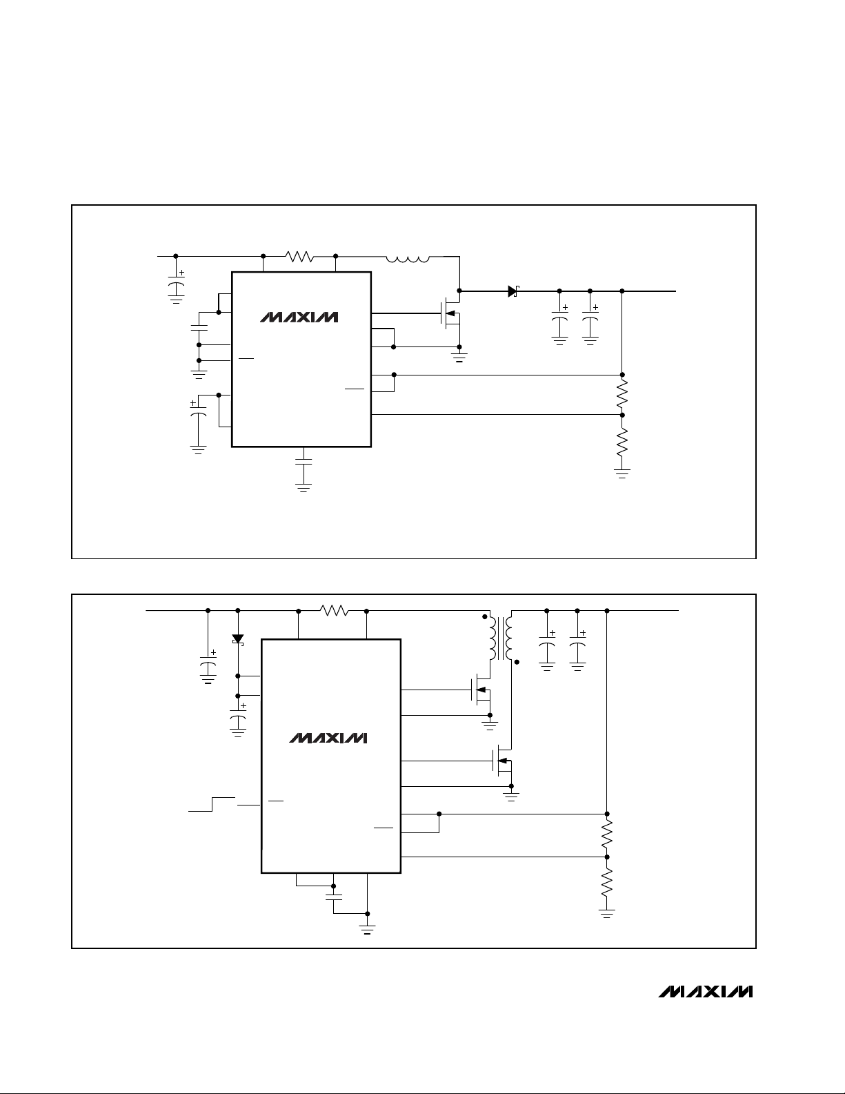
MAX796/MAX797/MAX799
Step-Down Controllers with
Synchronous Rectifier for CPU Power
28 ______________________________________________________________________________________
MAX797
CSL
CSH
SS
VL
SYNC
REF
GND
V+
Q1
FB
191k
49.9k
+12V AT 2A
BST
DH
LX
PGND
SKIP
SHDN
VIN
4.75V TO 6V
C2
150µFC3150µF
0.33µF
0.01Ω
0.01µF
C1
220µF
D1
4.7µF
L1
5µH
L1 = 2x SUMIDA CDRH125-100 IN PARALLEL
D1 = MOTOROLA MBR640
Q1 = MOTOROLA MTD20N03HDL
C1 = SANYO OS-CON 220µF, 10V
C2, C3 = SANYO OS-CON 150µF, 16V
Figure 16. 5V-to-12V PWM Boost Converter
MAX797
CSLCSH
VL
SYNC REF
GND
V+
Q1
T1
Q2
FB
200k
200k
OUTPUT
+5V AT 500mA
BST
CMPSH-3A
DH
LX
DL
PGND
SKIP
HI EFF
LOW IQ
SHDN
INPUT
3V TO 6.5V
4.7µF
0.33µF
33mΩ
220µF 220µF
100µF
Q1, Q2 = Si9410DY
T1 = COILTRONIX CTX 10-4
10µH PRIMARY, 1:1
START-UP SUPPLY VOLTAGE = 3.5V TYP
Figure 17. 90% Efficient, Low-Voltage PWM Flyback Converter (4 Cells to 5V)
____________________________________________Application Circuits (continued)
Page 29

MAX796/MAX797/MAX799
Step-Down Controllers with
Synchronous Rectifier for CPU Power
______________________________________________________________________________________ 29
MAX797
CSL
CSH
VL
SYNC REF
GND
TO
VL
V+
Q1
Q2
FB
1000pF
R1
63.4k
0.1%
R2
200k
0.1%
10k
OUTPUT
3.3V ±1.8%
REMOTE
SENSE
POINT
BST
DH
LX
DL
PGND
SKIP
SS
SHDN
INPUT
4.7µF
0.33µF
0.01µF
R
SENSE
V
OUT
USE EXTERNAL REFERENCE
(MAX872) FOR BETTER ACCURACY.
ADJUST RANGE = 2.5V TO 4V AS SHOWN.
OMIT R2 FOR V
OUT
= 2.5V.
= V
REF
(1 + –––)
R1
R2
L1
MAX495
51k
5%
200k
5%
51k
5%
Figure 18. High-Accuracy Adjustable-Output Application
MAX797
CSL
CSH
VL
1N5819
SYNC REF
GND
V+
Si9410
Si9410
FB
-5V AT 1.5A
BST
DH
LX
DL
PGND
SKIP
INPUT
4.5V TO 25V
SHDN
0.33µF
0.1µF 4.7µF
22µF
22µF
1N4148
L1
0.025Ω
150µF
150µF
L1 = DALE LPE6562-A093
Figure 19. Negative-Output (Inverting Topology) Power Supply
____________________________________________Application Circuits (continued)
Page 30

MAX796/MAX797/MAX799
Step-Down Controllers with
Synchronous Rectifier for CPU Power
30 ______________________________________________________________________________________
MAX797
CSL
CSH
FB
VL
SYNC
V+
Q1
Q2
1N4148
1N4148
D1
1N5819
T1
REF
GND
+5V OUTPUT
AT 3A
BST
DH
LX
DL
PGND
SKIP
SS
SHDN
INPUT
0.33µF
C1
2x 22µF
4.7µF
C2
220µF
0.1µF
0.01µF
0.1µF
100k
1%
100k
1%
10µH
1.91Ω, 1%
T1 = 1:70 5mm SURFACE-MOUNT TRANSFORMER
DALE LPE-3325-A087
Q1, Q2 = MMSF5N03 OR Si9410DY
Figure 20. Buck Converter with Low-Loss SMT Current-Sense Transformer
____________________________________________Application Circuits (continued)
MAX797
MAX495
CSL
CSH
VL
SYNC
FB
V+
N1
N2
D1
D2
1N5820
REF
GND
1.5V OUTPUT
AT 5A
DH
LX
DL
PGND
BST
SKIP
SS
ON/OFF
SHDN
INPUT
4.75V
TO 5.5V
4.7µF
0.1µF
C6
0.01µF
C2
2 x 220µF
OS-CON
C3
0.1µF
C5
0.33µF
L1
3.3µH
C7
330pF
R1
12mΩ
R6
49.9k
R7
124k
R5
150k
TO
VL
R3
66.5k
1%
R4
100k
1%
C1
220µF
OS-CON
REMOTE SENSE LINE
N1 = N2 = MTD20N03HDL
L1 = COILCRAFT DO3316-332
Figure 21. 1.5V GTL Bus Termination Supply
Page 31

MAX796/MAX797/MAX799
Step-Down Controllers with
Synchronous Rectifier for CPU Power
______________________________________________________________________________________ 31
MAX797
MAX495
CSL
0.1µF
0.01µF
0.01µF
4.7µF
I
OUT
2.5A
V
IN
10.5V to
28V
GNDFB
V+
0.33µF
0.33µF
L1
10µH
0.025Ω
SHDN
9
3
2
6
7
4
SYNC
SS
DL
5
7 4
1
6
13
PGND
12
LX
15
DH
16
SKIP
2
BST
14
VL
11
10
REF
3
CSH
8
3X
100µF
16V
2X
22µF
35V
1.0k
39k
D2
1.7Ω
T1
D1
D3
Q1
Q2
D1, D3 CENTRAL SEMI. CMPSH-3
D2 NIEC EC10QS02L, SCHOTTKY RECT.
L1 DALE IHSM-4825 10µH 15%
T1 DALE LPE-3325-A087, CURRENT TRANSFORMER, 1:70
Q1, Q2 MOTOROLA MMSF5N03HD
Figure 22. Battery-Charger Current Source
____________________________________________Application Circuits (continued)
Page 32

MAX796/MAX797/MAX799
Step-Down Controllers with
Synchronous Rectifier for CPU Power
32 ______________________________________________________________________________________
___________________Chip Topography
LX
SHDN
CSL
0.16O"
(4.064mm)
0.085"
(2.159mm)
FB CSH
BST
DL
PGND
VL
V+
DHSS
GND
SYNC
REF
SKIP
(SECFB)
( ) ARE FOR MAX796/MAX799 ONLY.
_Ordering Information (continued)
*Contact factory for dice specifications
MAX799EPE
MAX799ESE
MAX799MJE -55°C to +125°C
-40°C to +85°C
-40°C to +85°C 16 Plastic DIP
16 Narrow SO
16 CERDIP
MAX799CPE
MAX799CSE
MAX799C/D 0°C to +70°C
0°C to +70°C
0°C to +70°C 16 Plastic DIP
16 Narrow SO
Dice*
MAX797EPE
MAX797ESE
MAX797MJE -55°C to +125°C
-40°C to +85°C
-40°C to +85°C 16 Plastic DIP
16 Narrow SO
16 CERDIP
PART
MAX797CPE
MAX797CSE
MAX797C/D 0°C to +70°C
0°C to +70°C
0°C to +70°C
TEMP. RANGE PIN-PACKAGE
16 Plastic DIP
16 Narrow SO
Dice*
TRANSISTOR COUNT: 913
SUBSTRATE CONNECTED TO GND
 Loading...