

Page 1
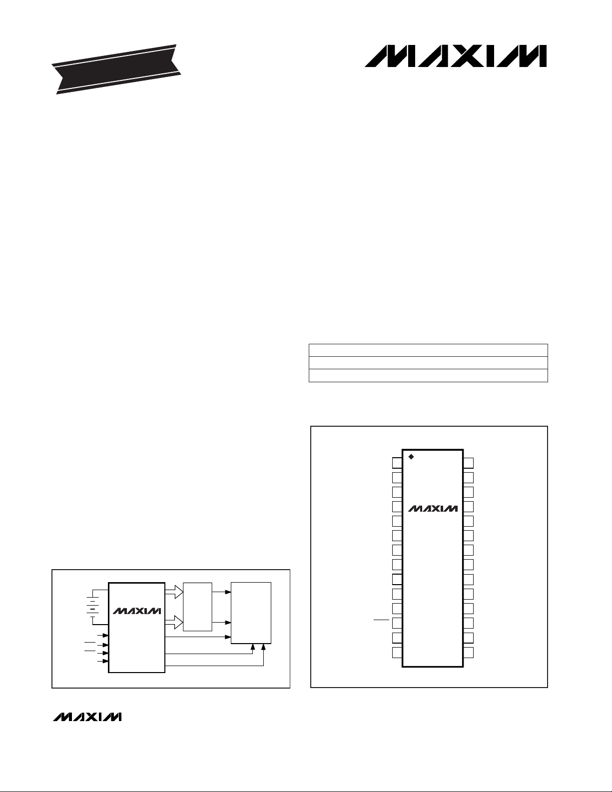
__________________General Description
The MAX786 is a system-engineered power-supply
controller for notebook computers or similar batterypowered equipment. It provides two high-performance
step-down (buck) pulse-width modulators (PWMs)
for +3.3V and +5V. Other features include dual,
low-dropout, micropower linear regulators for
CMOS/RTC back-up, and two precision low-batterydetection comparators.
High efficiency (95% at 2A; greater than 80% at loads
from 5mA to 3A) is achieved through synchronous rectification and PWM operation at heavy loads, and
Idle ModeTMoperation at light loads. The MAX786 uses
physically small components, thanks to high operating
frequencies (300kHz/200kHz) and a new current-mode
PWM architecture that allows for output filter capacitors
as small as 30µF per ampere of load. Line- and loadtransient responses are terrific, with a high 60kHz unitygain crossover frequency allowing output transients to
be corrected within four or five clock cycles. Low system cost is achieved through a high level of integration
and the use of low-cost, external N-channel MOSFETs.
Other features include low-noise, fixed-frequency PWM
operation at moderate to heavy loads, and a synchronizable oscillator for noise-sensitive applications such
as electromagnetic pen-based systems and communicating computers. The MAX786 is a monolithic,
BiCMOS IC available in fine-pitch, surface-mount
SSOP packages.
___________________________Applications
Notebook Computers
Portable Data Terminals
Communicating Computers
Pen-Entry Systems
________________________________Features
♦ Dual PWM Buck Controllers (+3.3V and +5V)
♦ Two Precision Comparators or Level Translators
♦ 95% Efficiency
♦ 420µA Quiescent Current, 70µA in Standby
(linear regulators alive)
♦ 25µA Shutdown Current (+5V linear alive)
♦ 5.5V to 30V Input Range
♦ Small SSOP Package
♦ Fixed Output Voltages:
3.3V (standard)
3.45V (High-Speed Pentium
™)
3.6V (PowerPC™)
_________________Ordering Information
MAX786
Dual-Output Power-Supply
Controller for Notebook Computers
_______________________________________________________________________
Maxim Integrated Products
1
19-0160; Rev 2; 4/97
_____________________Pin Configuration
28
27
26
25
24
23
22
21
1
2
3
4
5
6
7
8
FB3
DH3
LX3
BST3
D1
ON3
SS3
CS3
TOP VIEW
DL3
V+
VL
FB5
Q1
Q2
VH
D2
20
19
18
17
9
10
11
12
PGND
DL5
BST5
LX5
SHDN
SYNC
REF
GND
SSOP
MAX786
16
15
13
14
DH5
CS5
SS5
ON5
Idle Mode is a trademark of Maxim Integrated Products. Pentium is a trademark of Intel Corp. PowerPC is a trademark of IBM Corp.
________Typical Application Diagram
MAX786
5.5V
TO
30V
SHUTDOWN
POWER
SECTION
POWER-GOOD
LOW-BATTERY WARNING
µP
MEMORY
PERIPHERALS
+3.3V
+5V
5V ON/OFF
3.3V ON/OFF
SYNC
SUSPEND POWER
28 SSOP0°C to +70°CMAX786RCAI
28 SSOP0°C to +70°CMAX786CAI
PIN-PACKAGETEMP. RANGEPART
3.45V
3.3V
V
OUT
Ordering Information continued at end of data sheet.
EVALUATION KIT
INFORMATION INCLUDED
For free samples & the latest literature: http://www.maxim-ic.com, or phone 1-800-998-8800.
For small orders, phone 1-800-835-8769.
Page 2
MAX786
Dual-Output Power-Supply
Controller for Notebook Computers
2 ________________________________________________________________________________________________
Stresses beyond those listed under “Absolute Maximum Ratings” may cause permanent damage to the device. These are stress ratings only, and functional
operation of the device at these or any other conditions beyond those indicated in the operational sections of the specifications is not implied. Exposure to
absolute maximum rating conditions for extended periods may affect device reliability.
ELECTRICAL CHARACTERISTICS
(V+ = 15V, GND = PGND = 0V, IVL= I
REF
= 0mA,
SHDN
= ON3 = ON5 = 5V, other digital input levels are 0V or +5V,
T
A
= T
MIN
to T
MAX
, unless otherwise noted.)
ABSOLUTE MAXIMUM RATINGS
V+ to GND................................................................-0.3V to 36V
PGND to GND.......................................................................±2V
VL to GND..................................................................-0.3V to 7V
BST3, BST5 to GND.................................................-0.3V to 36V
LX3 to BST3 ...............................................................-7V to 0.3V
LX5 to BST5 ...............................................................-7V to 0.3V
Inputs/Outputs to GND
(D1, D2,
SHDN
, ON5, REF, SS5, CS5,
FB5, SYNC, CS3,FB3, SS3, ON3)............-0.3V to (VL + 0.3V)
VH to GND ...............................................................-0.3V to 20V
Q1, Q2 to GND............................................-0.3V to (VH + 0.3V)
DL3, DL5 to PGND.......................................-0.3V to (VL + 0.3V)
DH3 to LX3 ..............................................-0.3V to (BST3 + 0.3V)
DH5 to LX5 ..............................................-0.3V to (BST5 + 0.3V)
REF, VL Short to GND................................................Momentary
REF Current........................................................................20mA
VL Current ..........................................................................50mA
Continuous Power Dissipation (T
A
= +70°C)
SSOP (derate 9.52mW/°C above +70°C)....................762mW
Operating Temperature Ranges
MAX786CAI/MAX786_CAI .................................0°C to +70°C
MAX786EAI/MAX786_EAI...............................-40°C to +85°C
Lead Temperature (soldering, 10sec) ............................+300°C
MAX786S
MAX786R
MAX786
FB3 Output Voltage
3.46 3.65 3.75
V
0mV < (CS3-FB3) < 70mV, 6V < V + < 30V
(includes load and line regulation)
3.32 3.50 3.60
REF Load Regulation 30 75 mV0mA < IL< 5mA (Note 2)
PARAMETER
VL Output Voltage
MIN TYP MAX
4.5 5.5
UNITS
Current-Limit Voltage
V
80 100 120
VL Fault Lockout Voltage
mV
Line Regulation
3.6 4.2
0.03 %/V
Load Regulation 2.5
V
%
3.17 3.35 3.46
VL/FB5 Switchover Voltage
SS3/SS5 Source Current 2.5 4.0 6.5 µA
4.2 4.7 V
REF Output Voltage
SS3/SS5 Fault Sink Current 2
3.24 3.36
mA
V
REF Fault Lockout Voltage 2.4 3.2 V
Input Supply Range 5.5 30 V
FB5 Output Voltage 4.80 5.08 5.20 V
CONDITIONS
ON5 = ON3 = 0V, 5.5V < V+ < 30V, 0mA < IL< 25mA
CS3-FB3 or CS5-FB5
Falling edge, hysteresis = 1%
Either controller (V+ = 6V to 30V)
Either controller (CS_ -FB_ = 0mV to 70mV)
Rising edge of FB5, hysteresis = 1%
No external load (Note 1)
0mV < (CS5-FB5) < 70mV, 6V < V + < 30V
(includes load and line regulation)
Falling edge
V+ Shutdown Current 25 40 µA
–S—H—D—N–
= D1 = D2 = ON3 = ON5 = 0V, V+ = 30V
V+ Standby Current 70 120 µAD1 = D2 = ON3 = ON5 = 0V, V+ = 30V
Quiescent Power Consumption
(both PWM controllers on)
5.5 8.6 mW
D1 = D2 = 0V, FB5 = CS5 = 5.25V,
FB3 = CS3 = 3.5V
V+ Off Current 30 60 µAFB5 = CS5 = 5.25V, VL switched over to FB5
D1, D2 Trip Voltage 1.61 1.69 VFalling edge, hysteresis = 1%
D1, D2 Input Current ±100 nAD1 = D2 = 0V, 5V
3.3V AND 5V STEP-DOWN CONTROLLERS
INTERNAL REGULATOR AND REFERENCE
COMPARATORS
Page 3
MAX786
Dual-Output Power-Supply
Controller for Notebook Computers
_________________________________________________________________________________________________
3
Note 1: Since the reference uses VL as its supply, its V+ line regulation error is insignificant.
Note 2: The main switching outputs track the reference voltage. Loading the reference reduces the main outputs slightly according
to the closed-loop gain (AV
CL
) and the reference voltage load-regulation error. AVCLfor the +3.3V supply is unity gain.
AVCLfor the +5V supply is 1.54.
PARAMETER CONDITIONS MIN TYP MAX UNITS
Q1, Q2 Source Current VH = 15V, V
OUT
= 2.5V 12 20 30 µA
Q1, Q2 Sink Current VH = 15V, V
OUT
= 2.5V 200 500 1000 µA
Q1, Q2 Output High Voltage I
SOURCE
= 5µA, VH = 3V VH -0.5 V
Q1, Q2 Output Low Voltage I
SINK
= 20µA, VH = 3V 0.4 V
Quiescent VH Current VH = 18V, D1 = D2 = 5V, no external load 4 10 µA
OSCILLATOR AND INPUTS/OUTPUTS
Oscillator Frequency
SYNC = 3.3V 270 300 330
kHz
SYNC = 0V, 5V 170 200 230
SYNC High Pulse Width 200 ns
SYNC Low Pulse Width 200 ns
SYNC Rise/Fall Time Not tested 200 ns
Oscillator SYNC Range 240 350 kHz
Maximum Duty Cycle
SYNC = 3.3V 89 92
%
SYNC = 0V or 5V 92 95
Input Low Voltage
SHDN
, ON3, ON5, SYNC 0.8 V
Input High Voltage
SHDN
, ON3, ON5 2.4
V
SYNC VL -0.5
Input Current
SHDN
, ON3, ON5 VIN= 0V, 5V ±1 µA
DL3/DL5 Sink/Source Current V
OUT
= 2V 1 A
DH3/DH5 Sink/Source Current BST3-LX3 = BST5-LX5 = 4.5V, V
OUT
= 2V 1 A
DL3/DL5 On-Resistance High or low 7 Ω
DH3/DH5 On-Resistance High or low, BST3-LX3 = BST5-LX5 = 4.5V 7 Ω
ELECTRICAL CHARACTERISTICS (continued)
(V+ = 15V, GND = PGND = 0V, IVL= I
REF
= 0mA,
SHDN
= ON3 = ON5 = 5V, other digital input levels are 0V or +5V,
T
A
= T
MIN
to T
MAX
, unless otherwise noted.)
Page 4
MAX786
Dual-Output Power-Supply
Controller for Notebook Computers
4 _______________________________________________________________________________________
________________________________________________Typical Operating Characteristics
(Circuit of Figure 1, TA = +25°C, unless otherwise noted.)
EFFICIENCY vs. +5V OUTPUT
CURRENT, 300kHz
EFFICIENCY (%)
50
60
70
80
90
100
1m 10m 100m 1 10
+5V OUTPUT CURRENT (A)
VIN = 6V
VIN = 15V
VIN = 30V
+3.3V OFF
EFFICIENCY vs. +3.3V OUTPUT
CURRENT, 200kHz
EFFICIENCY (%)
50
60
70
80
90
100
1m
10m 100m 1 10
+3.3V OUTPUT CURRENT (A)
VIN = 6V
VIN = 15V
VIN = 30V
SYNC = 0V, +5V ON
EFFICIENCY vs. +3.3V OUTPUT
CURRENT, 300kHz
EFFICIENCY (%)
50
60
70
80
90
100
1m 10m 100m 1 10
+3.3V OUTPUT CURRENT (A)
VIN = 6V
VIN = 15V
VIN = 30V
+5V ON
SHUTDOWN SUPPLY CURRENT vs.
SUPPLY VOLTAGE
SHUTDOWN SUPPLY CURRENT (µA)
0
100
200
300
400
500
0
6 12 18 24 30
SUPPLY VOLTAGE (V)
SHDN = 0V
QUIESCENT SUPPLY CURRENT vs.
SUPPLY VOLTAGE
QUIESCENT SUPPLY CURRENT (mA)
0
1
2
18
19
0 6 12 18 24 30
SUPPLY VOLTAGE (V)
ON3 = ON5 = HIGH
STANDBY SUPPLY CURRENT vs.
SUPPLY VOLTAGE
STANDBY SUPPLY CURRENT (mA)
0
0.5
1.0
1.5
2.0
2.5
0 6 12 18 24 30
ON3 = ON5 = 0V
SUPPLY VOLTAGE (V)
MINIMUM VIN TO V
OUT
DIFFERENTIAL
vs. +5V OUTPUT CURRENT
MINIMUM V
IN
TO V
OUT
DIFFERENTIAL (V)
+5V OUTPUT CURRENT (A)
0
0.2
0.4
0.6
0.8
1.0
1m 10m 100m 1 10
300kHz
200kHz
+5V OUTPUT
STILL REGULATING
EFFICIENCY vs. +5V OUTPUT
CURRENT, 200kHz
EFFICIENCY (%)
50
60
70
80
90
100
1m 10m 100m 1 10
+5V OUTPUT CURRENT (A)
VIN = 6V
VIN = 30V
VIN = 15V
SYNC = 0V, +3.3V OFF
1000
0.1
100µ 10m 1
SWITCHING FREQUENCY vs.
LOAD CURRENT
10
LOAD CURRENT (A)
SWITCHING FREQUENCY (kHz)
100
1m 100m
SYNC = REF (300kHz)
ON3 = ON5 = 5V
+5V, VIN = 7.5V
1
+5V, VIN = 30V
+3.3V, VIN = 7.5V
Page 5
200µs/div
I
LOAD
= 100mA
V
IN
= 10V
IDLE MODE WAVEFORMS
+5V OUTPUT
50mV/div
2V/div
MAX786
Dual-Output Power-Supply
Controller for Notebook Computers
_______________________________________________________________________________________ 5
500ns/div
+5V OUTPUT CURRENT = 1A
V
IN
= 16V
PULSE-WIDTH MODULATION MODE WAVEFORMS
LX 10V/div
+5V OUTPUT
50mV/div
200µs/div
V
IN
= 15V
+3.3V LOAD-TRANSIENT RESPONSE
+3.3V OUTPUT
50mV/div
3A
0A
LOAD CURRENT
200µs/div
V
IN
= 15V
+5V LOAD-TRANSIENT RESPONSE
+5V OUTPUT
50mV/div
3A
0A
LOAD CURRENT
_________________________________Typical Operating Characteristics (continued)
(Circuit of Figure 1, TA = +25°C, unless otherwise noted.)
Page 6
MAX786
Dual-Output Power-Supply
Controller for Notebook Computers
6 _______________________________________________________________________________________
_________________________________Typical Operating Characteristics (continued)
(Circuit of Figure 1, TA = +25°C, unless otherwise noted.)
20µs/div
I
LOAD
= 2A
+5V LINE-TRANSIENT RESPONSE, RISING
VIN, 10V TO 16V
2V/div
+5V OUTPUT
50mV/div
20µs/div
I
LOAD
= 2A
+5V LINE-TRANSIENT RESPONSE, FALLING
VIN, 16V TO 10V
2V/div
+5V OUTPUT
50mV/div
20µs/div
I
LOAD
= 2A
+3.3V LINE-TRANSIENT RESPONSE, RISING
+3.3V OUTPUT
50mV/div
V
IN
, 10V TO 16V
2V/div
20µs/div
I
LOAD
= 2A
+3.3V LINE-TRANSIENT RESPONSE, FALLING
+3.3V OUTPUT
50mV/div
V
IN
, 16V TO 10V
2V/div
Page 7

MAX786
Dual-Output Power-Supply
Controller for Notebook Computers
_______________________________________________________________________________________ 7
PIN NAME FUNCTION
1 CS3 Current-sense input for +3.3V; +100mV = current limit level referenced to FB3.
2 SS3 Soft-start input for +3.3V. Ramp time to full current limit is 1ms/nF of capacitance to GND.
3 ON3 ON/
OFF
control input disables the +3.3V PWM. Tie directly to VL for automatic start-up.
4 D1 #1 level-translator/comparator noninverting input, threshold = +1.650V. Controls Q1. Tie to GND if unused.
5 D2 #2 level-translator/comparator noninverting input (see D1)
6 VH External positive supply-voltage input for the level translators/comparators
7 Q2
#2 level-translator/comparator output. Sources 20µA from VH when D2 is high. Sinks 500µA to GND
when D2 is low, even with VH = 0V.
8 Q1 #1 level translator/comparator output (see Q2)
9 GND Low-current analog ground
10 REF 3.3V reference output. Sources up to 5mA for external loads. Bypass to GND with 1µF/mA of load or
0.22µF minimum.
11 SYNC
Oscillator control/synchronization input. Connect to VL or GND for 200kHz; connect to REF for
300kHz. For external clock synchronization in the 240kHz to 350kHz range, a high-to-low transition
causes a new cycle to start.
12
SHDN
Shutdown control input, active low. Tie to VL for automatic start-up. The 5V VL supply stays active in
shutdown, but all other circuitry is disabled. Do not force
SHDN
higher than VL + 0.3V.
13 ON5 ON/
OFF
control input disables the +5V PWM supply. Tie to VL for automatic start-up.
14 SS5 Soft-start control input for +5V. Ramp time to full current limit is 1ms/nF of capacitance to GND.
15 CS5 Current-sense input for +5V; +100mV = current-limit level referenced to FB5.
16 DH5 Gate-drive output for the +5V high-side MOSFET
17 LX5 Inductor connection for the +5V supply
18 BST5 Boost capacitor connection for the +5V supply (0.1µF)
19 DL5 Gate-drive output for the +5V low-side MOSFET
20 PGND Power ground
21 FB5 Feedback and current-sense input for the +5V PWM
22 VL 5V logic supply voltage for internal circuitry. VL is always on and can source 5mA for external loads.
23 V+ Supply voltage input from battery, 5.5V to 30V
24 DL3 Gate-drive output for the +3.3V low-side MOSFET
25 BST3 Boost capacitor connection for the +3.3V supply (0.1µF)
26 LX3 Inductor connection for the +3.3V supply
27 DH3 Gate-drive output for the +3.3V high-side MOSFET
28 FB3 Feedback and current-sense input for the +5V PWM
_______________________________________________________________________Pin Description
Page 8

MAX786
Dual-Output Power-Supply
Controller for Notebook Computers
8 _______________________________________________________________________________________
The MAX786 has two close relatives: the MAX782 and
the MAX783. The MAX782 and MAX783 each include
an extra flyback winding regulator and linear regulators
for dual, +12V/programmable PCMCIA VPP outputs.
The MAX782/MAX783 data sheet contains extra applications information on the MAX786 not found in this
data sheet.
+3.3V Switch-Mode Supply
The +3.3V supply is generated by a current-mode,
PWM step-down regulator using two N-channel
MOSFETs, a rectifier, and an LC output filter (Figure 1).
The gate-drive signal to the high-side MOSFET, which
must exceed the battery voltage, is provided by
a boost circuit that uses a 100nF capacitor connected
to BST3.
_________________Detailed Description
The MAX786 converts a 5.5V to 30V input to four outputs
(Figure 1). It produces two high-power, PWM, switchmode supplies, one at +5V and the other at +3.3V. The
two supplies operate at either 300kHz or 200kHz,
allowing for small external components. Output current
capability depends on external components, and can
exceed 6A on each supply. An internal 5V, 5mA supply
(VL) and a 3.3V, 5mA reference voltage are also generated via linear regulators, as shown in Figure 2. Fault
protection circuitry shuts off the PWMs when the internal supplies lose regulation.
Two precision voltage comparators are also included.
Their output stages permit them to be used as level
translators for driving external N-channel MOSFETs in
load-switching applications, or for more conventional
logic signals.
MAX786
V+ VL
23 22
INPUT
5.5V TO 30V
(NOTE 1) C1
33µF
D2A
1N4148
C5
0.1µF
25
27
18
16
17
GND REF PGND
C3
1µF
+3.3V AT 5mA
BST3
DH3
LX3
BST5
DH5
LX5
9 10 20
N1
C9
0.01µF
+3.3V ON/OFF
+5V ON/OFF
SHUTDOWN
OSC SYNC
INPUT VOLTAGE RANGE 6.5V TO 30V
AS SHOWN. SEE
LOW-VOLTAGE
(6-CELL) OPERATION
SECTION FOR
DETAILS.
NOTE 1:
USE SHORT, KELVIN-CONNECTED PC
BOARD TRACES PLACED VERY CLOSE
TO ONE ANOTHER.
NOTE 2:
COMPARATOR SUPPLY INPUT
IN
OUT
COMPARATOR 1
IN
OUT
COMPARATOR 2
(NOTE 2)
C8
0.01µF
N4
D3
1N5819
L2
10µH
R2
25m
+5V
AT
3A
C6
330µF
+5V AT 5mA
4.7µF
C10
33µF
N2
D2B
1N4148
C4
0.1µF
2
3
13
12
11
14
6
4
8
5
7
SS3
ON3
ON5
SHDN
SYNC
SS5
VH
D1
Q1
D2
Q2
19
15
21
DL5
CS5
FB5
(NOTE 2)
N3
26
D1
1N5819
L1
10µH
R1
25mΩ
+3.3V
AT
3A
C12
150µF
24
1
28
DL3
CS3
FB3
C7
150µF
Figure 1. MAX786 Application Circuit
Page 9

MAX786
Dual-Output Power-Supply
Controller for Notebook Computers
_______________________________________________________________________________________ 9
A synchronous rectifier at LX3 keeps efficiency high by
clamping the voltage across the rectifier diode.
Maximum current limit is set by an external low-value
sense resistor, which prevents excessive inductor current during start-up or under short-circuit conditions.
Programmable soft-start is set by an optional external
capacitor; this reduces in-rush surge currents upon
start-up and provides adjustable power-up times for
power-supply sequencing purposes.
P
+5V LDO
LINEAR
REGULATOR
V+
VL
REF
SHDN
GND
+3.3V
REFERENCE
ON
3.3V
5V
4V
2.8V
SYNC
300kHz/200kHz
OSCILLATOR
ON
STANDBY
4.5V
FAULT
ON
3.3V
PWM
CONTROLLER
(SEE FIG. 3)
FB3
CS3
BST3
DH3
LX3
DL3
SS3
FB5
CS5
BST5
DH5
LX5
DL5
SS5
PGND
ON3
5V
PWM
CONTROLLER
(SEE FIG. 3)
ON
D1
D2
1.65V
1.65V
ON5
VH
Q1
Q2
Figure 2. MAX786 Block Diagram
Page 10

MAX786
Dual-Output Power-Supply
Controller for Notebook Computers
10 ______________________________________________________________________________________
+5V Switch-Mode Supply
The +5V output is produced by a current-mode, PWM
step-down regulator, which is nearly identical to the
+3.3V supply. The +5V supply’s dropout voltage, as
configured in Figure 1, is typically 400mV at 2A. As V+
approaches 5V, the +5V output gracefully falls with
V+ until the VL regulator output hits its undervoltagelockout threshold at 4V. At this point, the +5V supply
turns off.
The default frequency for both PWM controllers is
300kHz (with SYNC connected to REF), but 200kHz
may be used by connecting SYNC to GND or VL.
+3.3V and +5V PWM Buck Controllers
The two current-mode PWM controllers are identical
except for different preset output voltages (Figure 3).
Each PWM is independent except for being synchronized to a master oscillator and sharing a common reference (REF) and logic supply (VL). Each PWM can
be turned on and off separately via ON3 and ON5. The
PWMs are a direct-summing type, lacking a traditional integrator error amplifier and the phase shift
associated with it. They therefore do not require any
external feedback compensation components if the filter capacitor ESR guidelines given in the
Design
Procedure
are followed.
The main gain block is an open-loop comparator that
sums four input signals: an output voltage error signal,
current-sense signal, slope-compensation ramp, and
precision voltage reference. This direct-summing
method approaches the ideal of cycle-by-cycle control
of the output voltage. Under heavy loads, the controller
operates in full PWM mode. Every pulse from the oscillator sets the output latch and turns on the high-side
switch for a period determined by the duty cycle
(approximately V
OUT/VIN
). As the high-side switch turns
off, the synchronous rectifier latch is set and, 60ns later,
the low-side switch turns on (and stays on until the
beginning of the next clock cycle, in continuous mode,
or until the inductor current crosses through zero, in
discontinuous mode). Under fault conditions where the
inductor current exceeds the 100mV current-limit
threshold, the high-side latch is reset and the high-side
switch is turned off.
At light loads, the inductor current fails to exceed the
25mV threshold set by the minimum current comparator.
When this occurs, the PWM goes into idle mode, skipping most of the oscillator pulses in order to reduce the
switching frequency and cut back switching losses. The
oscillator is effectively gated off at light loads because
the minimum current comparator immediately resets the
high-side latch at the beginning of each cycle, unless the
FB_ signal falls below the reference voltage level.
Soft-Start/SS_ Inputs
Connecting capacitors to SS3 and SS5 allows gradual
build-up of the +3.3V and +5V supplies after ON3 and
ON5 are driven high. When ON3 or ON5 is low, the
appropriate SS capacitors are discharged to GND.
When ON3 or ON5 is driven high, a 4µA constant current source charges these capacitors up to 4V. The
resulting ramp voltage on the SS_ pins linearly increases the current-limit comparator setpoint so as to
increase the duty cycle to the external power MOSFETs
up to the maximum output. With no SS capacitors, the
circuit will reach maximum current limit within 10µs.
Soft-start greatly reduces initial in-rush current peaks
and allows start-up time to be programmed externally.
Synchronous Rectifiers
Synchronous rectification allows for high efficiency
by reducing the losses associated with the Schottky
rectifiers.
When the external power MOSFET N1 (or N2) turns off,
energy stored in the inductor causes its terminal voltage to reverse instantly. Current flows in the loop
formed by the inductor, Schottky diode, and load — an
action that charges up the filter capacitor. The Schottky
diode has a forward voltage of about 0.5V which,
although small, represents a significant power loss,
degrading efficiency. A synchronous rectifier, N3 (or
N4), parallels the diode and is turned on by DL3 (or
DL5) shortly after the diode conducts. Since the on
resistance (r
DS(ON)
) of the synchronous rectifier is very
low, the losses are reduced.
The synchronous rectifier MOSFET is turned off when
the inductor current falls to zero.
Cross conduction (or “shoot-through”) occurs if the
high-side switch turns on at the same time as the synchronous rectifier. The MAX786’s internal break-beforemake timing ensures that shoot-through does not occur.
The Schottky rectifier conducts during the time that neither MOSFET is on, which improves efficiency by preventing the synchronous-rectifier MOSFET’s lossy body
diode from conducting.
The synchronous rectifier works under all operating conditions, including discontinuous-conduction and idle mode.
Boost Gate-Driver Supply
Gate-drive voltage for the high-side N-channel switch is
generated with a flying-capacitor boost circuit as shown
in Figure 4. The capacitor is alternately charged from
the VL supply via the diode and placed in parallel with
the high-side MOSFET’s gate-source terminals. On startup, the synchronous rectifier (low-side) MOSFET forces
LX_ to 0V and charges the BST_ capacitor to 5V. On the
Page 11

MAX786
Dual-Output Power-Supply
Controller for Notebook Computers
______________________________________________________________________________________ 11
second half-cycle, the PWM turns on the high-side
MOSFET by connecting the capacitor to the MOSFET
gate by closing an internal switch between BST_ and
DH_. This provides the necessary enhancement voltage
to turn on the high-side switch, an action that “boosts”
the 5V gate-drive signal above the battery voltage.
Ringing seen at the high-side MOSFET gates (DH3 and
DH5) in discontinuous-conduction mode (light loads) is
a natural operating condition caused by the residual
energy in the tank circuit formed by the inductor and
stray capacitance at the LX_ nodes. The gate driver
negative rail is referred to LX_, so any ringing there is
directly coupled to the gate-drive supply.
1X
CS_
FB_
BST_
DH_
LX_
LEVEL
SHIFT
VL
SHOOTTHROUGH
CONTROL
DL_
PGND
LEVEL
SHIFT
Q
R
S
SYNCHRONOUS
RECTIFIER CONTROL
N
3.3V
1R
30R
VL
4µA
0mV TO 100mV
CURRENT
LIMIT
MINIMUM
CURRENT
(IDLE MODE)
25mV
SLOPE COMP
Σ
REF, 3.3V
(OR INTERNAL
5V REFERENCE)
MAIN PWM
COMPARATOR
60kHz
LPF
R
S
Q
OSC
SS_
ON_
Figure 3. PWM Controller Block Diagram
Page 12

MAX786
Dual-Output Power-Supply
Controller for Notebook Computers
12 ______________________________________________________________________________________
Modes of Operation
PWM Mode
Under heavy loads —over approximately 25% of full load
—the +3.3V and +5V supplies operate as continuouscurrent PWM supplies (see
Typical Operating Char-
acteristics
). The duty cycle (%ON) is approximately:
%ON = V
OUT/VIN
Current flows continuously in the inductor: First, it
ramps up when the power MOSFET conducts; then, it
ramps down during the flyback portion of each cycle
as energy is put into the inductor and then discharged into the load. Note that the current flowing
into the inductor when it is being charged is also flowing into the load, so the load is continuously receiving
current from the inductor. This minimizes output ripple and maximizes inductor use, allowing very small
physical and electrical sizes. Output ripple is primarily
a function of the filter capacitor (C7 or C6) effective
series resistance (ESR) and is typically under 50mV
(see the
Design Procedure
section). Output ripple is
worst at light load and maximum input voltage.
Idle Mode
Under light loads (<25% of full load), efficiency is further enhanced by turning the drive voltage on and off
for only a single clock period, skipping most of the
clock pulses entirely. Asynchronous switching, seen as
“ghosting” on an oscilloscope, is thus a normal operating
condition whenever the load current is less than
approximately 25% of full load.
At certain input voltage and load conditions, a transition
region exists where the controller can pass back and
forth from idle mode to PWM mode. In this situation,
short bursts of pulses occur that make the current
waveform look erratic, but do not materially affect the
output ripple. Efficiency remains high.
Current Limiting
The voltage between CS3 (CS5) and FB3 (FB5) is continuously monitored. An external, low-value shunt resistor
is connected between these pins, in series with the
inductor, allowing the inductor current to be continuously
measured throughout the switching cycle. Whenever this
voltage exceeds 100mV, the drive voltage to the external
high-side MOSFET is cut off. This protects the MOSFET,
the load, and the battery in case of short circuits or temporary load surges. The current-limiting resistors R1 and
R2 are typically 25mΩ for 3A load current.
Oscillator Frequency; SYNC Input
The SYNC input controls the oscillator frequency.
Connecting SYNC to GND or to VL selects 200kHz operation; connecting to REF selects 300kHz operation. SYNC
can also be driven with an external 240kHz to 350kHz
CMOS/TTL source to synchronize the internal oscillator.
Normally, 300kHz is used to minimize the inductor and
filter capacitor sizes, but 200kHz may be necessary for
low input voltages (see
Low-Voltage
(6-Cell) Operation
).
Comparators
Two noninverting comparators can be used as
precision voltage comparators or high-side drivers. The
supply for these comparators (VH) is brought out and may
be connected to any voltage between +3V and +19V
irrespective of V+. The noninverting inputs (D1-D2) are
high impedance, and the inverting input is internally connected to a 1.650V reference. Each output (Q1-Q2)
sources 20µA from VH when its input is above 1.650V, and
sinks 500µA to GND when its input is below 1.650V. The
Q1-Q2 outputs can be fixed together in wired-OR
configuration since the pull-up current is only 20µA.
Connecting VH to a logic supply (5V or 3V) allows the
comparators to be used as low-battery detectors. For
driving N-channel power MOSFETs to turn external
loads on and off, VH should be 6V to 12V higher than
the load voltage. This enables the MOSFETs to be fully
turned on and results in low r
DS(ON)
.
The comparators are always active when V+ is above
+4V, even when VH is 0V. Thus, Q1-Q2 will sink current
to GND even when VH is 0V, but they will only source
current from VH when VH is above approximately 1.5V.
If Q1 or Q2 is externally pulled above VH, an internal
diode conducts, pulling VH a diode drop below the
output and powering anything connected to VH. This
voltage will also power the other comparator outputs.
LEVEL
TRANSLATOR
PWM
VL
BST_
DH_
LX_
DL_
VL
BATTERY
INPUT
VL
Figure 4. Boost Supply for Gate Drivers
Page 13

MAX786
Dual-Output Power-Supply
Controller for Notebook Computers
______________________________________________________________________________________ 13
Table 1. Surface-Mount Components
(See Figure 1 for Standard Application Circuit.)
Internal VL and REF Supplies
An internal linear regulator produces the 5V used by the
internal control circuits. This regulator’s output is available on pin VL and can source 5mA for external loads.
Bypass VL to GND with 4.7µF. To save power, when the
+5V switch-mode supply is above 4.5V, the internal linear regulator is turned off and the high-efficiency +5V
switch-mode supply output is connected to VL.
The internal 3.3V bandgap reference (REF) is powered
by the internal 5V VL supply. It can furnish up to 5mA.
Bypass REF to GND with 0.22µF, plus 1µF/mA of load
current. The main switching outputs track the reference
voltage. Loading the reference will reduce the main
outputs slightly, according to the reference load-regulation error.
Both the VL and REF outputs remain active, even when
the switching regulators are turned off, to supply memory keep-alive power (see
Shutdown Mode
section).
These linear-regulator outputs can be directly connected
to the corresponding step-down regulator outputs (i.e.,
REF to +3.3V, VL to +5V) to keep the main supplies alive
in standby mode. However, to ensure start-up, standby
load currents must not exceed 5mA on each supply.
Fault Protection
The +3.3V and +5V PWM supplies and the comparators are disabled when either of two faults is present:
VL < +4.0V or REF < +2.8V (85% of its nominal value).
__________________Design Procedure
Figure 1’s schematic and Table 2’s component list
show values suitable for a 3A, +5V supply and a 3A,
+3.3V supply. This circuit operates with input voltages
from 6.5V to 30V, and maintains high efficiency with
output currents between 5mA and 3A (see the
Typical
Operating Characteristics
). This circuit’s components
may be changed if the design guidelines described in
this section are used —but before beginning the
design, the following information should be firmly
established:
COMPONENT SPECIFICATION MANUFACTURER PART NO.
C1, C10 33µF, 35V tantalum capacitors
AVX TPSE226M035R0100
Sprague 595D336X0035R
C2 4.7µF, 6V tantalum capacitor
AVX TAJB475M016
Sprague 595D475X0016A
C3 1µF, 20V tantalum capacitor
AVX TAJA105M025
Sprague 595D105X0020A2B
C4, C5 0.1µF, 16V ceramic capacitors Murata-Erie GRM42-6X7R104K50V
C6 330µF, 10V tantalum capacitor Sprague 595D337X0010R
C7, C12 150µF, 10V tantalum capacitors Sprague 595D157X0010D
C8, C9 0.01µF, 16V ceramic capacitors Murata-Erie GRM42-6X7R103K50V
D2A, D2B 1N4148-type dual diodes Central Semiconductor CMPD2836
D1, D3 1N5819 SMT diodes Nihon EC10QS04
L1, L2 10µH, 2.65A inductors Sumida CDR125-100
N1–N4 N-channel MOSFETs (SO-8) Siliconix Si9410DY
R1, R2 0.025Ω, 1% (SMT) resistors IRC LR2010-01-R025-F
COMPANY
FACTORY FAX
USA PHONE
[COUNTRY CODE]
AVX [1] (803) 626-3123
(803) 946-0690
(800) 282-4975
Central Semiconductor [1] (516) 435-1824 (516) 435-1110
IRC [1] (512) 992-3377 (512) 992-7900
Murata-Erie [1] (814) 238-0490 (814) 237-1431
Nihon [81] 3-3494-7414 (805) 867-2555
Siliconix [1] (408) 970-3950 (408) 988-8000
Sprague [1] (603) 224-1430 (603) 224-1961
Sumida [81] 3-3607-5144 (847) 956-0666
Table 2. Component Suppliers
Page 14

MAX786
Dual-Output Power-Supply
Controller for Notebook Computers
14 ______________________________________________________________________________________
V
IN(MAX)
, the maximum input (battery) voltage. This
value should include the worst-case conditions under
which the power supply is expected to function, such
as no-load (standby) operation when a battery charger
is connected but no battery is installed. V
IN(MAX)
cannot
exceed 30V.
V
IN(MIN)
, the minimum input (battery) voltage. This
value should be taken at the full-load operating current under the lowest battery conditions. If V
IN(MIN)
is
below about 6.5V, the filter capacitance required to
maintain good AC load regulation increases, and the
current limit for the +5V supply has to be increased
for the same load level.
Inductor (L1, L2)
Three inductor parameters are required: the inductance
value (L), the peak inductor current (I
LPEAK
), and the
coil resistance (RL). The inductance is:
(V
OUT
) (V
IN(MAX)
- V
OUT
)
L = ————————————
(V
IN(MAX)
) (f) (I
OUT
) (LIR)
where: V
OUT
= output voltage (3.3V or 5V);
V
IN(MAX)
= maximum input voltage (V);
f = switching frequency, normally 300kHz;
I
OUT
= maximum DC load current (A);
LIR = ratio of inductor peak-to-peak AC
current to average DC load current, typically 0.3.
A higher value of LIR allows smaller inductance, but
results in higher losses and higher ripple.
The highest peak inductor current (I
LPEAK
) equals the DC
load current (I
OUT
) plus half the peak-to-peak AC inductor
current (I
LPP
). The peak-to-peak AC inductor current is
typically chosen as 30% of the maximum DC load current, so the peak inductor current is 1.15 times I
OUT
.
The peak inductor current at full load is given by:
(V
OUT
) (V
IN(MAX)
- V
OUT
)
I
LPEAK
= I
OUT
+ —————————————.
(2) (f) (L) (V
IN(MAX)
)
The coil resistance should be as low as possible,
preferably in the low milliohms. The coil is effectively in
series with the load at all times, so the wire losses alone
are approximately:
Power loss = (I
OUT
2
) (RL).
In general, select a standard inductor that meets the L,
I
LPEAK
, and RLrequirements (see Tables 1 and 2). If a
standard inductor is unavailable, choose a core with an
LI2parameter greater than (L) (I
LPEAK
2
), and use the
largest wire that will fit the core.
Current-Sense Resistors (R1, R2)
The sense resistors must carry the peak current in the
inductor, which exceeds the full DC load current. The
internal current limiting starts when the voltage across
the sense resistors exceeds 100mV nominally, 80mV
minimum. Use the minimum value to ensure adequate
output current capability: For the +3.3V supply, R1 =
80mV / (1.15 x I
OUT
); for the +5V supply, R2 =
80mV/(1.15 x I
OUT
), assuming that LIR = 0.3.
Since the sense resistance values (e.g., R1 = 25mΩ for
I
OUT
= 3A) are similar to a few centimeters of narrow
traces on a printed circuit board, trace resistance can
contribute significant errors. To prevent this, Kelvin connect the CS_ and FB_ pins to the sense resistors; i.e.,
use separate traces not carrying any of the inductor or
load current, as shown in Figure 5.
Run these traces parallel at minimum spacing from one
another. The wiring layout for these traces is critical for
stable, low-ripple outputs (see the
Layout and
Grounding
section).
MOSFET Switches (N1-N4)
The four N-channel power MOSFETs are usually identical and must be “logic-level” FETs; that is, they must
be fully on (have low r
DS(ON)
) with only 4V gate-
source drive voltage. The MOSFET r
DS(ON)
should
ideally be about twice the value of the sense resistor.
MOSFETs with even lower r
DS(ON)
have higher gate
capacitance, which increases switching time and
transition losses.
MOSFETs with low gate-threshold voltage specifications (i.e., maximum V
GS(TH)
= 2V rather than 3V) are
preferred, especially for high-current (5A) applications.
Output Filter Capacitors (C6, C7, C12)
The output filter capacitors determine the loop stability
and output ripple voltage. To ensure stability, the minimum capacitance and maximum ESR values are:
V
REF
CF> —————————————
(V
OUT
) (RCS) (2) (π) (GBWP)
and,
(V
OUT
) (RCS)
ESRCF< ——————
V
REF
where: CF= output filter capacitance (F);
V
REF
= reference voltage, 3.3V;
V
OUT
= output voltage, 3.3V or 5V;
R
CS
= sense resistor (Ω);
GBWP = gain-bandwidth product, 60kHz;
ESR
CF
= output filter capacitor ESR (Ω).
Page 15

MAX786
Dual-Output Power-Supply
Controller for Notebook Computers
______________________________________________________________________________________ 15
Be sure to select output capacitors that satisfy both
the minimum capacitance and maximum ESR requirements. To achieve the low ESR required, it may be
appropriate to use a capacitance value 2 or 3 times
larger than the calculated minimum.
The output ripple in continuous-current mode is:
V
OUT(RPL)
= I
LPP(MAX)
x (ESR
CF
+ 1/(2 x π x f x CF) ).
In idle-mode, the ripple has a capacitive and resistive
component:
(4) (10-4) (L)
V
OUT(RPL)
(C) = ——————— x
(R
CS
2
) (CF)
1 1
(
——— + —————
)
Volts
V
OUT
VIN- V
OUT
(0.02) (ESRCF)
V
OUT(RPL)
(R) = ———————- Volts
R
CS
The total ripple, V
OUT(RPL)
, can be approximated as
follows:
if V
OUT(RPL)
(R) < 0.5 V
OUT(RPL)
(C),
then V
OUT(RPL)
= V
OUT(RPL)
(C),
otherwise, V
OUT(RPL)
= 0.5 V
OUT(RPL)
(C) +
V
OUT(RPL)
(R).
Diodes D1 and D3
Use 1N5819s or similar Schottky diodes. D1 and D3
conduct only about 3% of the time, so the 1N5819’s
1A current rating is conservative. The voltage rating
of D1 and D3 must exceed the maximum input supply
voltage from the battery. These diodes must
be Schottky diodes to prevent the lossy MOSFET
body diodes from turning on, and they must be
placed physically close to their associated synchronous rectifier MOSFETs.
Soft-Start Capacitors (C8, C9)
A capacitor connected from GND to either SS pin
causes that supply to ramp up slowly. The ramp time to
full current limit, tSS, is approximately 1ms for every nF
of capacitance on SS_, with a minimum value of 10µs.
Typical capacitor values are in the 10nF to 100nF
range; a 5V rating is sufficient.
Because this ramp is applied to the current-limit circuit,
the actual time for the output voltage to ramp up
depends on the load current and output capacitor
value. Using Figure 1’s circuit with a 2A load and no SS
capacitor, full output voltage is reached about 600µs
after ON_ is driven high.
Boost Capacitors (C4, C5)
Capacitors C4 and C5 store the boost voltage and provide the supply for the DH3 and DH5 drivers. Use 0.1µF
and place each within 10mm of the BST_ and LX_ pins.
Boost Diodes (D1A, D1B)
Use high-speed signal diodes; e.g., 1N4148 or
equivalent.
Bypass Capacitors
Input Filter Capacitors (C1, C10)
Use at least 3µF/W of output power for the input filter
capacitors, C1 and C10. They should have less than
150mΩ ESR, and should be located no further than
10mm from N1 and N2 to prevent ringing. Connect the
negative terminals directly to PGND. Do not exceed the
surge current ratings of input bypass capacitors.
Shutdown Mode
Shutdown (
SHDN
= low) forces both PWMs off and disables the REF output and both comparators (Q1 = Q2
= 0V). Supply current in shutdown mode is typically
25µA. The VL supply remains active and can source
25mA for external loads. Note that the VL load capability is higher in shutdown and standby modes than when
the PWMs are operating (25mA vs. 5mA). Standby
mode is achieved by holding ON3 and ON5 low while
SHDN
is high. This disables both PWMs, but keeps VL,
REF, and the precision comparators alive. Supply current
in standby mode is typically 70µA.
MAX786
KELVIN SENSE TRACES
SENSE RESISTOR
MAIN CURRENT PATH
FAT, HIGH-CURRENT TRACES
Figure 5. Kelvin Connections for the Current-Sense Resistors
Page 16
MAX786
V+ VL
23 22
V+
C1
33µF
35V
R9
1k
R10
OPEN
6
D2
25
18
16
17
19
15
10
11
7
8
SS3
GND
PGND
BST3
DH3
LX3
DL3
CS3
FB3
ON3
ON5
SHDN
D1
BST5
DH5
LX5
DL5
CS5
FB5
REF
SYNC
Q2
Q1
2
14
20
3.3V
OUT
C7
150µF
10V
C12
150µF
10V
L1
10µH
D1
1N5819
SHDN
D1
SYNC
Q1
Q2
C3
1µF
20V
D3
1N5819
L2
10µH
R2
0.025Ω
5V
OUT
C6
330µF
10V
C2
4.7µF
C10
33µF
35V
D2
R1
0.025Ω
N1
N3
D2
R61MR51MR81MR7
1M
R4
1M
9
27
26
24
1
28
3
13
12
4
5
C9
0.01µF
SW1CSW1A
SW1B
R3
1M
21
VH
D2
SS5
VREF (3.3V)
SW1D
N2
N4
C4
0.1µF
N1 – N4 = Si9410DY
D2 = BAW56L OR TWO 1N4148s
VL (5V)
C8
0.01µF
ON3
ON5
C5
0.1µF
MAX786
Dual-Output Power-Supply
Controller for Notebook Computers
16 ______________________________________________________________________________________
Other ways to shut down the MAX786 are suggested
in the applications section of the MAX782/MAX783
data sheet.
__________Applications Information
Low-Voltage (6-Cell) Operation
The standard application circuit can be configured to
accept input voltages from 5.5V to 12V by changing
the oscillator frequency to 200kHz and increasing the
+5V filter capacitor to 660µF. This allows stable operation at 5V loads up to 2A (the 3.3V side requires no
changes and still delivers 3A).
Figure 6. MAX786 EV Kit Schematic
Table 3. EV Kit Power-Supply Controls (SW1)
SWITCH NAME FUNCTION
ON
SETTING
OFF
SETTING
1 SHDN
Enable shutdown
mode
Operate Shutdown
2 ON3
Enable 3.3V
power supply
3.3V ON 3.3V OFF
3 ON5
Enable 5.0V
power supply
5V ON 5V OFF
4 SYNC Oscillator 200kHz 300kHz
Page 17

MAX786
Dual-Output Power-Supply
Controller for Notebook Computers
______________________________________________________________________________________ 17
_________________EV Kit Information
The MAX786 evaluation kit (EV kit) embodies the
standard application circuit, with some extra pullup and pull-down resistors needed to set default logic
signal levels. The board comes configured to accept
battery input voltages between 6.5V and 30V, and provides up to 25W of output power. All functions are con-
trolled by standard CMOS/TTL logic levels or DIP
switches. The kit can be reconfigured for lower battery
voltages by setting the oscillator to 200kHz and
increasing the 5V output filter capacitor value.
The D1 and D2 comparators can be used as precision
voltage detectors by installing resistor dividers at each
input.
Figure 7. MAX786 EV Kit Top Component Layout and Silk
Screen, Top View
Figure 8. MAX786 EV Kit Ground Plane (Layers 2 and 3),
Top View
Figure 9. MAX786 EV Kit Top Layer (Layer 1), Top View
1.0"
1.0"
1.0"
Page 18

MAX786
Dual-Output Power-Supply
Controller for Notebook Computers
18 ______________________________________________________________________________________
Figure 11. MAX786 EV Kit, Bottom Layer (Layer 4), Top View
Figure 10. MAX786 EV Kit, Bottom Component Layout and Silk
Screen, Bottom View
1.0"
1.0"
Page 19

MAX786
Dual-Output Power-Supply
Controller for Notebook Computers
______________________________________________________________________________________ 19
______________________Chip Topography
LX3
ON3
D1
DH5
CS5ON5
SHDN
SS5
D2
VH
Q2
Q1
GND
REF
SYNC
0.181"
(4.597mm)
BST3
DL3
V+
VL
FB5
DL5
BST5
LX5
SS3
CS3 FB3
DH3
PGND
0.109"
(2.769mm)
TRANSISTOR COUNT: 1294
SUBSTRATE CONNECTED TO GND
Page 20

MAX786
Dual-Output Power-Supply
Controller for Notebook Computers
________________________________________________________Package Information
*Contact factory for dice specifications.
__Ordering Information (continued)
EV KIT TEMP. RANGE BOARD TYPE
0°C to +70°C Surface MountMAX786EVKIT-SO
Dice*0°C to +70°CMAX786C/D
28 SSOP0°C to +70°CMAX786SCAI
PIN-PACKAGETEMP. RANGEPART
—
3.6V
V
OUT
28 SSOP-40°C to +85°CMAX786REAI
28 SSOP-40°C to +85°CMAX786EAI
3.45V
3.3V
28 SSOP-40°C to +85°CMAX786SEAI 3.6V
Maxim cannot assume responsibility for use of any circuitry other than circuitry entirely embodied in a Maxim product. No circuit patent licenses are
implied. Maxim reserves the right to change the circuitry and specifications without notice at any time.
20
____________________Maxim Integrated Products, 120 San Gabriel Drive, Sunnyvale, CA 94086 408-737-7600
© 1997 Maxim Integrated Products Printed USA is a registered trademark of Maxim Integrated Products.
SSOP.EPS
 Loading...