

Page 1
RDY5
19-0045; Rev 1; 5/94
Evaluation Kit
Information Included
Triple-Output Power-Supply Controller
for Notebook Computers
_______________General Description
The MAX783 is a system-engineered power-supply controller
for notebook computers or similar battery-powered equipment.
It provides two high-performance step-down (buck) pulsewidth modulators (PWMs) for +3.3V/+5V and dual PCMCIA
VPP outputs powered by an integral flyback winding controller.
Other functions include dual, low-dropout, micropower linear
regulators for CMOS/RTC back up, and two precision lowbattery-detection comparators.
High efficiency (95% at 2A, greater than 80% at loads from
5mA to 3A) is achieved through synchronous rectification
and PWM operation at heavy loads, and Idle-Mode
TM
operation at light loads. The MAX783 uses physically small
components, thanks to high operating frequencies
(300kHz/200kHz) and a new current-mode PWM architecture that allows for output filter capacitors as small as 30µF
per ampere of load. Line- and load-transient responses
are terrific, with a high 60kHz unity-gain crossover frequency that allows output transients to be corrected within four
or five clock cycles. Low system cost is achieved through
a high level of integration and the use of low-cost external
N-channel MOSFETs. The integral flyback winding controller provides a low-cost, +15V high-side output that regulates even in the absence of a load on the main output.
Other features include low-noise, fixed-frequency PWM
operation at moderate to heavy loads and a synchronizable
oscillator for noise-sensitive applications such as electromagnetic pen-based systems and communicating computers. The MAX783 is similar to the MAX782, except the flyback winding is on the 3.3V inductor instead of the 5V
inductor, the VPP outputs can be optionally programmed to
3.3V, and the device may be completely shut down.
________________________Applications
Notebook Computers
Portable Data Terminals
Communicating Computers
Pen-Entry Systems
_______Typical Application Diagram
+3.3V
+5V
µP
MEMORY
PERIPHERALS
DUAL
PCMCIA
SLOTS
5.5V
TO
30V
VPP
CONTROL
ON3
ON5
SYNC
SHDN
™
Idle-Mode is a trademark of Maxim Integrated Products. Pentium is a trademark of Intel. PowerPC is a trademark of IBM.
MAX783
4
POWER
SECTION
SUSPEND POWER
LOW-BATTERY WARNING
VPP (0V/3.3V/5V/12V)
VPP (0V/3.3V/5V/12V)
________________________________________________________________
Call toll free 1-800-998-8800 for free samples or literature.
____________________________Features
♦ Dual PWM Buck Controllers (+3.3V and +5V)
♦ Dual PCMCIA VPP Outputs (0V/3.3V/5V/12V)
♦ Two Precision Comparators or Level Translators
♦ Power-Ready Status Output (
♦ 95% Efficiency
)
♦ Optimized for 6-Cell Applications
♦ 420µA Quiescent Current;
70µA in Standby (linear regulators alive)
25µA Shutdown Current
♦ 5.5V to 30V Input Range
♦ Small SSOP Package
♦ Fixed Output Voltages Available:
3.3V (standard)
3.45V (High-Speed Pentium™)
3.6V (PowerPC™)
______________Ordering Information
PIN-PACKAGETEMP. RANGEPART
36 SSOP0°C to +70°CMAX783CBX
36 SSOP0°C to +70°CMAX783RCBX
Ordering Information continued on last page.
__________________Pin Configuration
TOP VIEW
ON3
SHDN
RDY5
VPPA
VDD
VPPB
GND
REF
SYNC
DA1
DA0
DB1
DB0
1
2
D1
3
D2
4
VH
5
Q2
6
7
Q1
MAX783
8
9
10
11
12
13
14
15
16
17
18
36
SS3
CS3
35
FB3
34
DH3
33
LX3
32
31
BST3
30
DL3
29
V+
28
VL
27
FB5
26
PGND
25
DL5
24
BST5
23
LX5
22
DH5
21
CS5
20
SS5
19
ON5
SSOP
Maxim Integrated Products
V
OUT
3.3V
3.45V
MAX783
1
Page 2
Triple-Output Power-Supply Controller
for Notebook Computers
ABSOLUTE MAXIMUM RATINGS
V+ to GND.................................................................-0.3V, +36V
PGND to GND........................................................................±2V
VL to GND ...................................................................-0.3V, +7V
BST3, BST5 to GND ..................................................-0.3V, +36V
LX3 to BST3.................................................................-7V, +0.3V
LX5 to BST5.................................................................-7V, +0.3V
Inputs/Outputs to GND
MAX783
(D1, D2, S—H—D—N–, ON5, REF, SYNC, DA1, DA0, DB1, DB0, ON5,
SS5, CS5, FB5, R—D—Y—5–, CS3, FB3, SS3, ON3).-0.3V, (VL + 0.3V)
VDD to GND.................................................................-0.3V, 20V
VPPA, VPPB to GND.....................................-0.3V, (VDD + 0.3V)
VH to GND...................................................................-0.3V, 20V
Q1, Q2 to GND................................................-0.3V, (VH + 0.3V)
DL3, DL5 to PGND..........................................-0.3V , (VL + 0.3V)
Stresses beyond those listed under “Absolute Maximum Ratings” may cause permanent damage to the device. These are stress ratings only, and functional
operation of the device at these or any other conditions beyond those indicated in the operational sections of the specifications is not implied. Exposure to
absolute maximum rating conditions for extended periods may affect device reliability.
ELECTRICAL CHARACTERISTICS
(V+ = 15V, GND = PGND = 0V, IVL= I
T
= T
to T
A
MIN
3.3V AND 5V STEP-DOWN CONTROLLERS
Input Supply Range
FB5 Output Voltage
FB3 Output Voltage
Line Regulation
Current-Limit Voltage
15V FLYBACK CONTROLLER
VDD Regulation Setpoint
VDD Shunt Setpoint
VDD Shunt Current
Quiescent VDD Current
PCMCIA REGULATORS (Note 1)
VPPA/VPPB Output Voltage
, unless otherwise noted.)
MAX
PARAMETER
0mV < (CS5-FB5) < 70mV, 6V < V + < 30V
(includes load and line regulation)
0mV < (CS3-FB3) < 70mV, 6V < V + < 30V
(includes load and line regulation)
Either controller (0mV to 70mV)
Either controller (6V to 30V)
CS3-FB3 or CS5-FB5
CS3-FB3 (VDD < 13V, flyback mode)
Falling edge, hysteresis = 1%
Rising edge, hysteresis = 1%
VDD = 20V
VDD = 18V, ON3 = ON5 = 5V, VPPA/VPPB programmed to
12V with no external load
VDD = 18V, ON3 = ON5 = 5V, VPPA/VPPB programmed to
0V
Program to 12V, 13V < VDD < 19V, 0mA < IL< 60mA
Program to 5V, 13V < VDD < 19V, 0mA < IL< 60mA
Program to 3.3V, 13V < VDD < 19V, 0mA < IL< 60mA
Program to 0V, 13V < VDD < 19V, 0mA < IL< 0.3mA
= 0mA, S—H—D—N–= ON3 = ON5 = 5V, other digital input levels are 0V or +5V,
REF
CONDITIONS
DH3 to LX3..................................................-0.3V, (BST3 + 0.3V)
DH5 to LX5..................................................-0.3V, (BST5 + 0.3V)
REF, VL, VPP Short to GND........................................Momentary
REF Current.........................................................................20mA
VL Current...........................................................................50mA
VPPA, VPPB Current.........................................................100mA
Continuous Power Dissipation (TA= +70°C)
SSOP (derate 11.76mW/°C above +70°C) ...................762mW
Operating Temperature Ranges:
MAX783CBX/MAX783_CBX.................................0°C to +70°C
MAX783EBX/MAX783_EBX ..............................-40°C to +85°C
Storage Temperature Range.............................-65°C to +160°C
Lead Temperature (soldering, 10sec).............................+300°C
UNITS
MAX783
MAX783R
MAX783S
MIN TYP MAX
3.17 3.35 3.46
3.32 3.50 3.60
3.46 3.65 3.75
2.5Load Regulation
80 100 120
-50 -100 -160
2SS3/SS5 Fault Sink Current
13 14
18 20
140 300
11.60 12.10 12.50
4.85 5.05 5.20
3.17 3.30 3.43
-0.30 0.30
V5.5 30
V4.80 5.08 5.20
V
%
%/V0.03
mV
µA2.5 4.0 6.5SS3/SS5 Source Current
mA
V
V
mA23
µA
µA15 30Off VDD Current
V
2 _______________________________________________________________________________________
Page 3
Triple-Output Power-Supply Controller
for Notebook Computers
ELECTRICAL CHARACTERISTICS (continued)
(V+ = 15V, GND = PGND = 0V, IVL= I
T
= T
to T
A
MIN
INTERNAL REGULATOR AND REFERENCE
VL Output Voltage
VL Fault Lockout Voltage
VL/FB5 Switchover Voltage
(also R—D—Y—5–Trip Voltage)
REF Output Voltage 3.24 3.36µAV
REF Fault Lockout Voltage
REF Load Regulation 30 75 mV
Shutdown V+ Current
Standby V+ Current
Quiescent Power Consumption
(both controllers on)
Off V+ Current
COMPARATORS
D1, D2 Trip Voltage
D1, D2 Input Current
Q1, Q2 R—D—Y—5–Source Current
Q1, Q2 R—D—Y—5–Sink Current
Q1, Q2, R—D—Y—5–Output High Voltage
Q1, Q2, R—D—Y—5–Output Low Voltage
Quiescent VH Current
OSCILLATOR AND INPUTS/OUTPUTS
Oscillator Frequency
SYNC High Pulse Width 200 ns
SYNC Low Pulse Width 200 ns
SYNC Rise/Fall Time
Oscillator SYNC Range
Maximum Duty Cycle
Input Low Voltage 0.8
Input High Voltage
Input Current
, unless otherwise noted.)
MAX
PARAMETER
ON5 = ON3 = 0V, 5.5V < V+ < 30V, 0mA < IL< 25mA
Falling edge, hysteresis = 1%
Rising edge of FB5, hysteresis = 1%
No external load (Note 2)
Falling edge
0mA < IL< 5mA (Note 3)
–S—H—D—N–
DB1 = 0V, V+ = 30V
D1 = D2 = ON3 = ON5 = DA0 = DA1 = DB0 = DB1 = 0V,
V+ = 30V
D1 = D2 = D3 = DA0 = DA1 = DB0 = DB1 = 0V,
FB5 = CS5 = 5.25V, FB3 = CS3 = 3.5V
FB5 = CS5 = 5.25V, VL switched over to FB5
Falling edge, hysteresis = 1%
D1 = D2 = 0V to 5V
VH = 15V, V
VH = 15V, V
I
SOURCE
I
SINK
VH = 18V, D1 = D2 = 5V, no external load
SYNC = 3.3V
SYNC = 0V or 5V
SYNC = 3.3V
SYNC = 0V or 5V
S—H—D—N–, ON3, ON5, DA0, DA1, DB0, DB1, SYNC
S—H—D—N–, ON3, ON5, DA0, DA1, DB0, DB1
SYNC
S—H—D—N–, ON3, ON5, DA0, DA1, DB0, DB1, VIN= 0V or 5V
= 0mA, S—H—D—N–= ON3 = ON5 = 5V, other digital input levels are 0V or +5V,
REF
CONDITIONS
= D1 = D2 = ON3 = ON5 = DA0 = DA1 = DB0 =
= 2.5V
OUT
2.5V
OUT
= 5µA, VH = 3V
= 20µA, VH = 3V
MIN TYP MAX
4.5 5.5 V
3.6 4.2 V
4.2 4.7 V
2.4 3.2 V
25 40
70 110 µA
5.2 8.6
30 60
1.61 1.69
±100 nA
12 20 30 µA
200 500 1000%µA
VH - 0.5 V
0.4 V
410µA
270 300 330
170 200 230
200 nsNot tested
240 350
89 92
92 95
2.4
VL - 0.5
±1 µA
MAX783
UNITS
µA
mW
V
kHz
kHz
V
V
_______________________________________________________________________________________ 3
Page 4
Triple-Output Power-Supply Controller
for Notebook Computers
ELECTRICAL CHARACTERISTICS (continued)
(V+ = 15V, GND = PGND = 0V, IVL= I
T
= T
to T
A
MIN
, unless otherwise noted.)
MAX
PARAMETER
DL3/DL5 Sink/Source Current V
OUT
DH3/DH5 Sink/Source Current BST3-LX3 = BST5-LX5 = 4.5V, V
MAX783
DL3/DL5 On-Resistance High or low 7 Ω
DH3/DH5 On-Resistance High or low, BST3-LX3 = BST5-LX5 = 4.5V 7 Ω
Note 1: Output current is further limited by maximum allowable package power dissipation.
Note 2: Because the reference uses VL as its supply, the REF line regulation error is insignificant.
Note 3: The main switching outputs track the reference voltage. Loading the reference reduces the main outputs slightly according
to the closed-loop gain (AV
AVCLfor the +5V supply is 1.54.
) and the reference voltage load regulation error. AVCLfor the +3.3V supply is unity gain.
CL
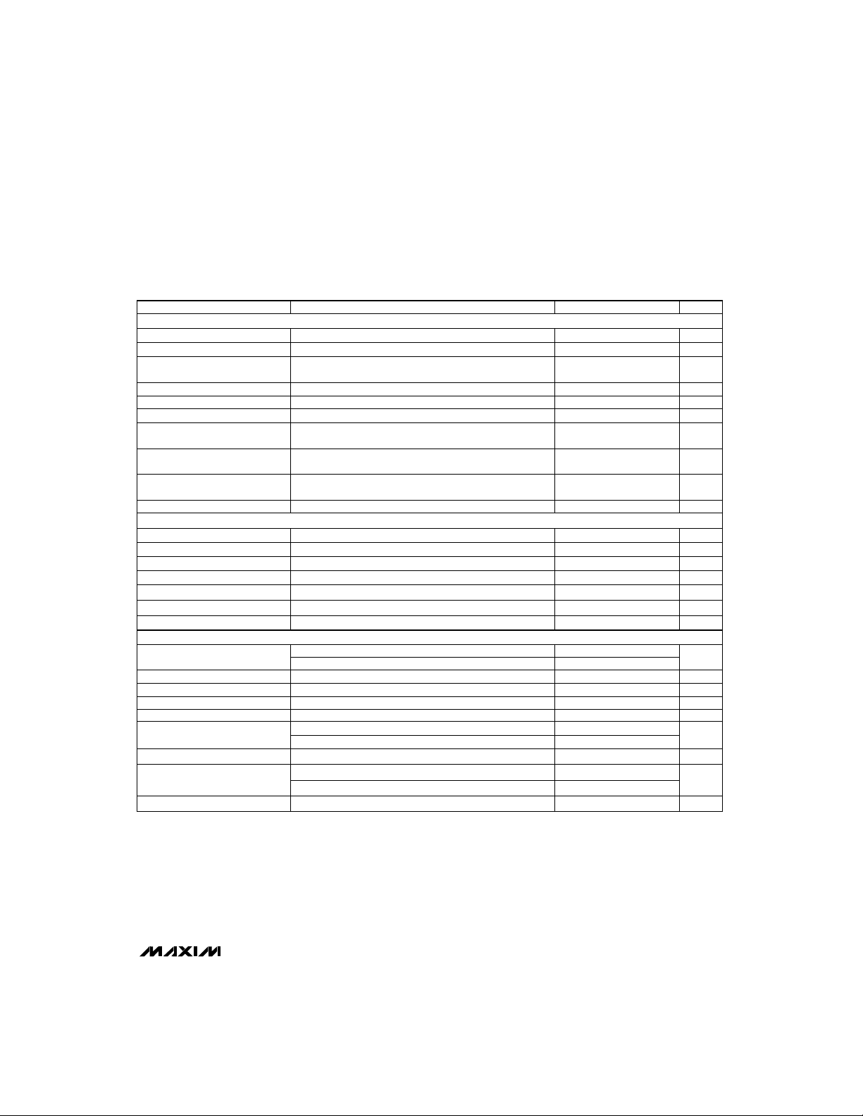
__________________________________________Typical Operating Characteristics
(Circuit of Figure 1, Transpower TTI5902 transformer, TA = +25°C, unless otherwise noted.)
= 0mA, S—H—D—N–= ON3 = ON5 = 5V, other digital input levels are 0V or +5V,
REF
CONDITIONS UNITS
MIN TYP MAX
= 2V 1 A
= 2V 1 A
OUT
100
90
80
70
EFFICIENCY (%)
60
50
1m
EFFICIENCY vs.
+5V OUTPUT CURRENT
V+ = 6V
V+ = 15V
N1-N4 = IRF7101
ON3 = LOW
F = 200kHz
10m 1
100m
+5V OUTPUT CURRENT (A)
QUIESCENT SUPPLY CURRENT vs.
SUPPLY VOLTAGE
14
13
ON3 = ON5 = HIGH
2
1
QUIESCENT SUPPLY CURRENT (mA)
0
0 6 12 18 24 30
SUPPLY VOLTAGE (V)
MAX183 5
10
100
90
80
70
EFFICIENCY (%)
60
50
1m
EFFICIENCY vs.
+3.3V OUTPUT CURRENT
V+ = 6V
V+ = 15V
N1-N4 = IRF7101
ON3 = ON5 = HIGH
F = 200kHz
10m 1
+3.3V OUTPUT CURRENT (A)
100m
MAXIMUM +15V VDD OUTPUT CURRENT vs.
500
MAX183 6
400
300
200
100
MAXIMUM +15V LOAD CURRENT (mA)
10
2.5
2.0
1.5
1.0
0.5
STANDBY SUPPLY CURRENT (mA)
0
0 6 12 18 24 30
0
STANDBY SUPPLY CURRENT vs.
SUPPLY VOLTAGE
ON3 = ON5 = 0V
SUPPLY VOLTAGE (V)
SUPPLY VOLTAGE
>
VDD
+13V
+3.3V REGULATING
+3.3V LOAD = 0A
05 20
+3.3V LOAD = 3A
10 15
SUPPLY VOLTAGE (V)
4 _______________________________________________________________________________________
Page 5
Triple-Output Power-Supply Controller
for Notebook Computers
____________________________Typical Operating Characteristics (continued)
(Circuit of Figure 1, Transpower TTI5902 transformer, TA = +25°C, unless otherwise noted.)
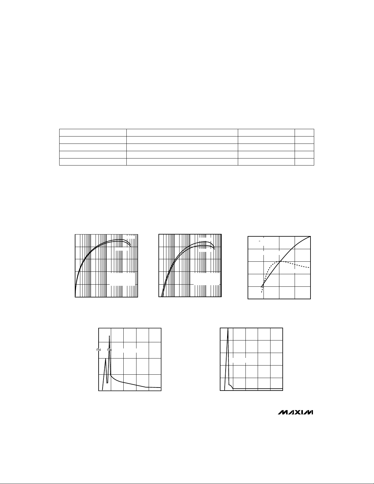
SHUTDOWN SUPPLY CURRENT vs.
SUPPLY VOLTAGE
500
400
300
200
100
SHUTDOWN SUPPLY CURRENT (µA)
0
SHDN = 0V
0
612182430
SUPPLY VOLTAGE (V)
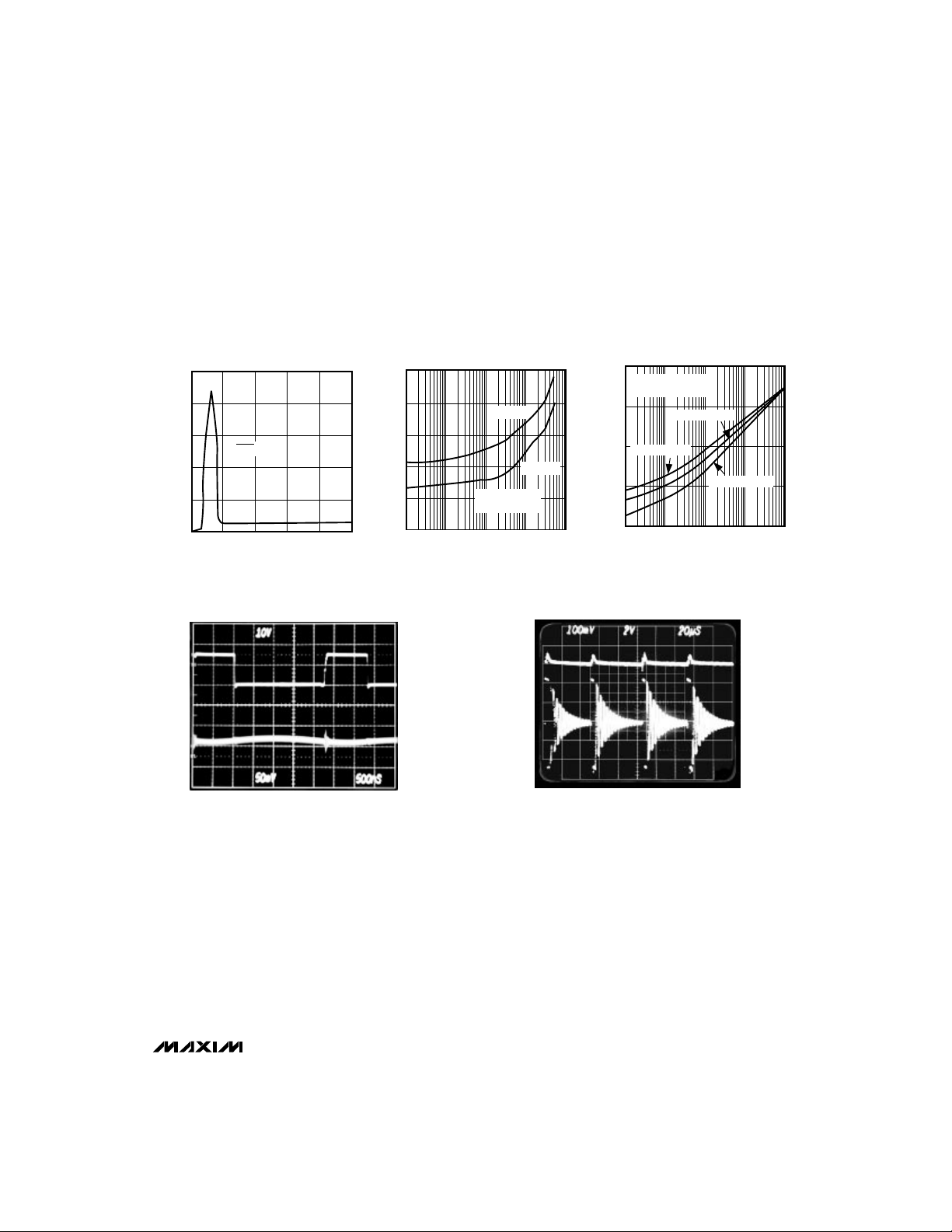
PULSE-WIDTH MODULATION MODE WAVEFORMS
MINIMUM VIN TO V
vs. +5V OUTPUT CURRENT
1.0
0.8
0.6
DIFFERENTIAL (V)
OUT
0.4
TO V
IN
0.2
MINIMUM V
0
1m 10m 100m 1 10
+5V OUTPUT CURRENT (A)
LX VOLTAGE
10V/div
+5V OUTPUT
VOLTAGE
50mV/div
DIFFERENTIAL
OUT
300kHz
+5V OUTPUT
STILL REGULATING
200kHz
SWITCHING FREQUENCY (kHz)
IDLE-MODE WAVEFORMS
SWITCHING FREQUENCY vs.
1000
100
10
1
0.1
100µ 10m 1
LOAD CURRENT
SYNC = REF (300kHz)
ON3 = ON5 = HIGH
+5V, VIN = 7.5V
+5V, VIN = 30V
1m 100m
LOAD CURRENT (A)
+3.3V, VIN = 7.5V
+5V OUTPUT
50mV/div
2V/div
MAX783
I
V
LOAD
IN
= 1A
= 16V
500ns/div
I
LOAD
V
IN
= 10V
= 100mA
200µs/div
_______________________________________________________________________________________
5
Page 6
Triple-Output Power-Supply Controller
for Notebook Computers
____________________________Typical Operating Characteristics (continued)
(Circuit of Figure 1, Transpower TTI5902 transformer, TA = +25°C, unless otherwise noted.)
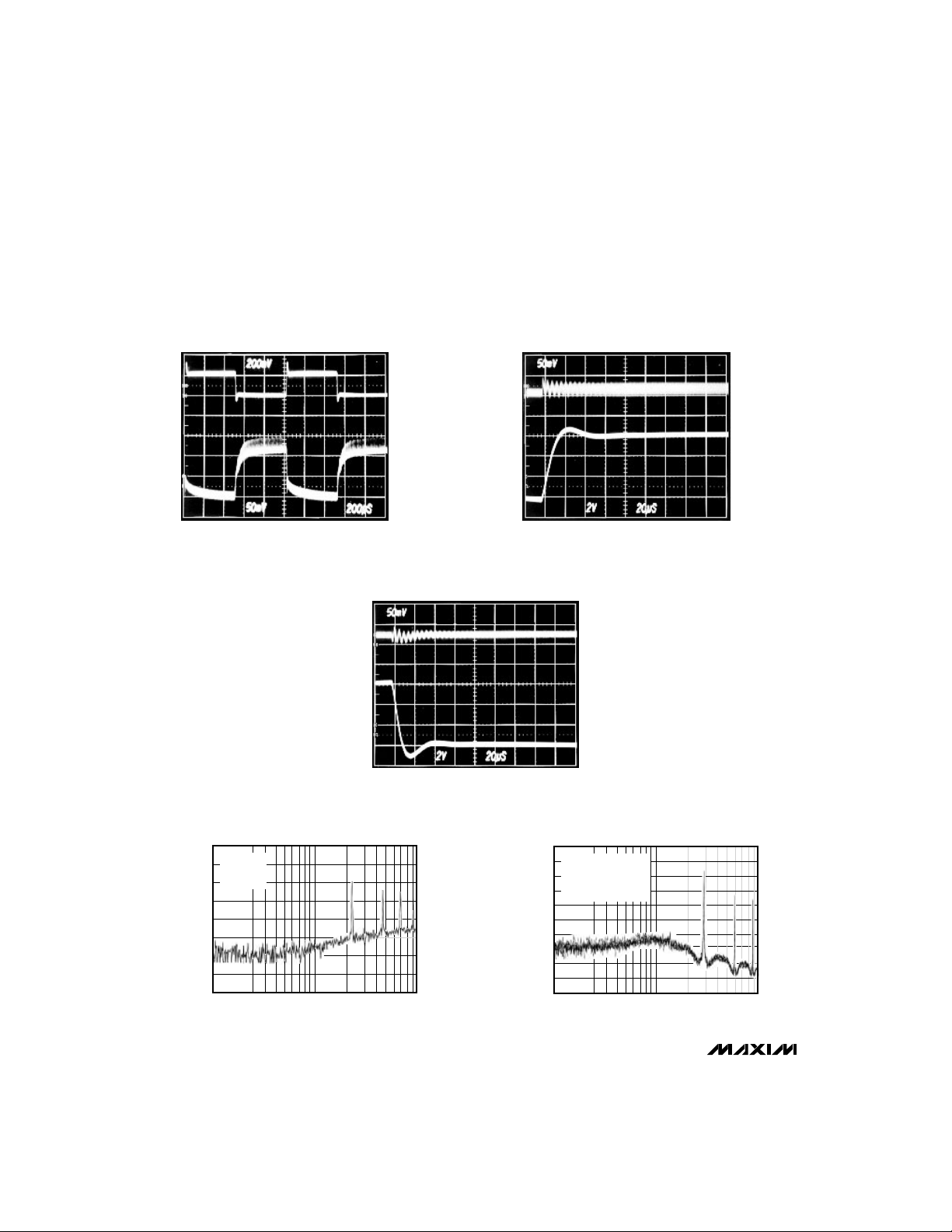
+5V LOAD-TRANSIENT RESPONSE
MAX783
V
= 15V
IN
)
30
VIN = 10V
RMS
20
V
OUT
I
10
OUT
0
-10
-20
-30
OUTPUT VOLTAGE NOISE (dBmV
1
200µs/div
OUTPUT NOISE SPECTRUM
= 5V
= 50mA
10 100
FREQUENCY (kHz)
3A
LOAD CURRENT
0A
+5V OUTPUT
50mV/div
I
LOAD
+5V LINE-TRANSIENT RESPONSE, FALLING
I
LOAD
= 2A
20µs/div
)
RMS
OUTPUT VOLTAGE NOISE (dBmV
+5V LINE-TRANSIENT RESPONSE, RISING
20µs/div
= 2A
+5V OUTPUT
50mV/div
VIN, 16V TO 10V
2V/div
100k 1M
FREQUENCY (Hz)
30
VIN = 8V TO 12V
20
(PLOTS SUPERIMPOSED)
10
= 5V
V
OUT
0
= 1A
I
OUT
-10
-20
-30
-40
-50
-60
10k
OUTPUT NOISE SPECTRUM
+5V OUTPUT
50mV/div
VIN, 10V TO 16V
2V/div
6 _______________________________________________________________________________________
Page 7
Triple-Output Power-Supply Controller
for Notebook Computers
______________________________________________________________Pin Description
PIN
15-18
NAME FUNCTION
1 ON3 ON/O—F—F–control input to disable the +3.3V PWM. Tie directly to VL for automatic start-up.
Shutdown control input, low-true logic. Tie to VL for automatic start-up. The 5V VL supply stays active in
2 S—H—D—N
3 D1
4 D2 #2 level-translator/comparator noninverting input (see D1).
5 VH External positive supply voltage input for the level translators/comparators and R—D—Y—5–output.
6 Q2
7 Q1 #1 level translator/comparator output (see Q2).
8 R—D—Y—5
9 VPPA 0V, 3.3V, 5V, 12V switchable PCMCIA VPP output. Sources 60mA. Controlled by DA0 and DA1.
10 VDD
11 VPPB 0V, 3.3V, 5V, 12V switchable PCMCIA VPP output. Sources 60mA. Controlled by DB0 and DB1.
12 GND Low-current analog ground. Feedback reference point for all outputs.
13 REF
14 SYNC
19 ON5 ON/O—F—F–control input to disable the +5V PWM supply. Tie to VL for automatic start-up.
20 SS5 Soft-start control input for +5V. Ramp time to full current limit is 1ms/nF of capacitance to GND.
21 CS5 Current-sense input for +5V. Current limit level is +100mV referred to FB5.
22 DH5 Gate-drive output for the +5V high-side MOSFET.
23 LX5 Inductor connection for the +5V supply.
24 BST5 Boost capacitor connection for the +5V supply (0.1µF).
25 DL5 Gate-drive output for the +5V low-side MOSFET.
26 PGND Power ground
27 FB5 Feedback and current-sense input for the +5V PWM.
28 VL 5V logic supply voltage for internal circuitry. VL is always on and can source 5mA for external loads.
29 V+ Supply voltage input from battery, 5.5V to 30V
30 DL3 Gate-drive output for the +3.3V low-side MOSFET.
31 BST3 Boost capacitor connection for the +3.3V supply (0.1µF).
32 LX3 Inductor connection for the +3.3V supply.
33 DH3 Gate-drive output for the +3.3V high-side MOSFET.
34 FB3 Feedback and current-sense input for the +3.3V PWM.
35 CS3 Current-sense input for +3.3V, current limit level is +100mV referred to FB3.
36 SS3 Soft-start input for +3.3V. Ramp time to full current limit is 1ms/nF of capacitance to GND.
–
–
DA1, DA0,
DB1, DB0
shutdown. Don't force S—H—D—N–higher than VL + 0.5V.
#1 level-translator/comparator noninverting input, threshold = +1.650V. Controls Q1. Tie to GND if
unused.
#2 level-translator/comparator output. Sources 20µA from VH when D2 is high. Sinks 500µA to GND when
D2 is low, even with VH = 0V.
Power-good indication for the main +5V supply. Low indicates greater than 4.5V at the +5V output.
Swings 0V to VH.
+15V flyback input (feedback). A weak shunt regulator conducts 3mA to GND when VDD exceeds 19V.
VDD serves as the supply input for the VPP linear regulators.
3.3V reference output sources up to 5mA for external loads. Bypass to GND with 1µF/mA of load or
0.22µF minimum
Oscillator control/synchronization input. Connect to VL or GND for 200kHz; connect to REF for 300kHz.
For external clock synchronization in the 240kHz to 350kHz range, a high-to-low transition starts a new cycle.
PCMCIA digital control inputs with industry-standard coding (see Table 1).
MAX783
_______________________________________________________________________________________ 7
Page 8
Triple-Output Power-Supply Controller
for Notebook Computers
Table 1. Truth Table for VPP Control Pins
D_0 D_1 VPP
0 0 0V
0 1 5V
1 0 12V
MAX783
1 1 3.3V
_______________Detailed Description
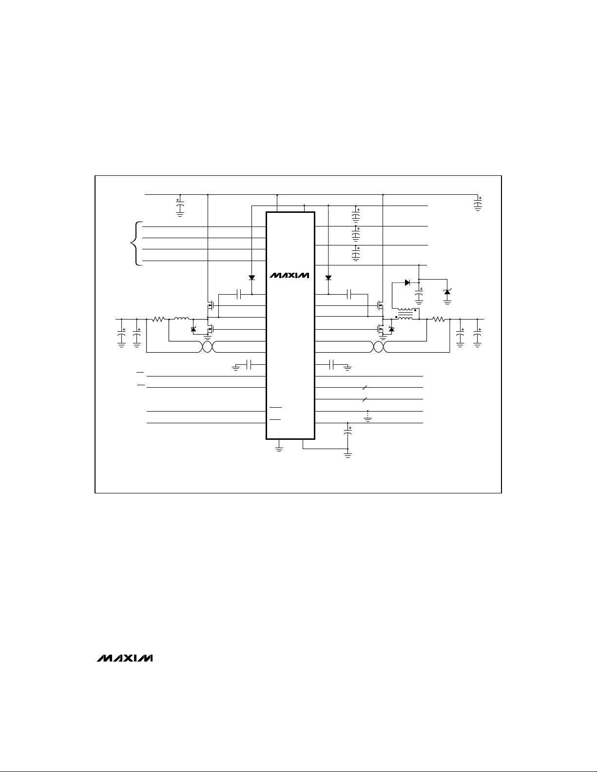
The MAX783 converts a 5.5V to 30V input to six outputs
(Figure 1). It produces two high-power, PWM switchmode supplies, one at +5V and the other at +3.3V. The
two supplies operate at either 300kHz or 200kHz, allowing for small external components. Output current capability depends on external components, and can exceed
6A on each supply. Two 12V VPP outputs, an internal 5V,
25mA supply (VL) and a 3.3V, 5mA reference voltage
are also generated via linear regulators (Figure 2). Faultprotection circuitry shuts off the PWM and high-side supply when the internal supplies lose regulation.
Two precision voltage comparators are also included.
Their output stages permit them to be used as level
translators for driving external N-channel MOSFETs in
load-switching applications, or for more conventional
logic signals.
The MAX783 is capable of accepting input voltages
from 5.5V to 30V, but is optimized for the lower end of
this range because the +15V flyback winding controller
is appended to the +3.3V buck supply. This architecture
allows for lower input voltages than are possible with the
MAX782 sister chip, which puts the winding on the +5V
side, while maintaining high +15V load capability.
However, the MAX783’s transformer has a higher turns
ratio (4:1 vs. 2:1), which leads to higher interwinding
capacitance as well as higher switching noise amplitudes at the transformer secondary when the input voltage is high. Therefore, the MAX783 standard application circuit is optimized with external components for
low-voltage (6-8 cell) designs with maximum input voltages of 20V and less. The MAX783 itself can easily
accept 30V inputs, but expect to see more noise and
higher voltage swings at the transformer secondary
under these conditions. The inductor and filter capacitor
values may also require some adjustment for inputs
greater than 20V; see the
The +5V supply is generated by a current-mode PWM
step-down regulator using two N-channel MOSFETs, a
rectifier, plus an LC output filter (Figure 1). The gatedrive signal to the high-side MOSFET, which must
exceed the battery voltage, is provided by a boost cir-
Design Procedure
section.
+5V Switch-Mode Supply
cuit that uses a 100nF capacitor connected to BST5.
The +5V supply’s dropout voltage, as configured in
Figure 1, is typically 400mV at 2A. As V+ approaches
5V, the +5V output falls with V+ until the VL regulator
output hits its undervoltage lockout threshold at 4V. At
this point, the +5V supply turns off.
A synchronous rectifier at LX5 keeps efficiency high by
effectively clamping the voltage across the rectifier
diode. Maximum current limit is set by an external lowvalue sense resistor, which prevents excessive inductor
current during start-up or under short-circuit conditions.
Programmable soft-start is set by an optional external
capacitor; this reduces in-rush surge currents upon
start-up and provides adjustable power-up times for
power-supply sequencing purposes.
+3.3V Switch-Mode Supply
The +3.3V output is produced by a current-mode PWM
step-down regulator similar to the +5V supply. The +3.3V
supply uses a transformer primary winding as its inductor; the secondary is used for the 15V VDD supply.
The default switching frequency for both PWM controllers
is 200kHz (with SYNC connected to GND or VL), but
300kHz may be used by connecting SYNC to REF.
+3.3V and +5V PWM Buck Controllers
The two current-mode PWM buck controllers are nearly
identical except for different preset output voltages and
the addition of a flyback winding control loop to the
3.3V side. Each PWM is independent, except both are
synchronized to a master oscillator and share a common reference (REF) and logic supply (VL). Each PWM
can be turned on and off separately via ON3 and ON5.
The PWMs are a direct-summing type, lacking a traditional integrator-type error amplifier and the phase shift
associated with it. They therefore do not require external feedback compensation components if you follow
the filter capacitor ESR guidelines in the
Procedure
The main gain block is an open-loop comparator that
sums four input signals: output voltage error signal,
current-sense signal, slope-compensation ramp, and
precision reference voltage. This direct-summing
method approaches the ideal of cycle-by-cycle control
of the output voltage. Under heavy loads, the controller
operates in full PWM mode. Every pulse from the oscillator sets the output latch and turns on the high-side
switch for a period determined by the duty factor
(approximately V
off, the synchronous rectifier latch is set; 60ns later, the
low-side switch turns on. The low-side switch stays on
until the beginning of the next clock cycle (in continuous mode) or until the inductor current crosses through
.
). As the high-side switch turns
OUT/VIN
Design
8 _______________________________________________________________________________________
Page 9
Triple-Output Power-Supply Controller
for Notebook Computers
MAX783
BATTERY INPUT
5.5V TO 30V
(NOTE 1)
VPP
CONTROL
INPUTS
+5V
at
3A
C3
330µF
+3.3V ON/OFF
+5V ON/OFF
SHUTDOWN
5V POWERGOOD
C1–C6 = SPRAGUE 595D or AVX TPS SERIES
N1–N4 = Si9410DY or IRF7101 (BOTH SECTIONS)
D1A, D1B = LOW-POWER SCHOTTKY (CMPSH3 OR EQUIVALENT)
FOR V
NOTE 1: BATTERY VOLTAGE RANGE 6V to 20V WITH COMPONENTS SHOWN.
NOTE 2: KEEP KELVIN-CONNECTED CURRENT-SENSE TRACES SHORT AND CLOSE TOGETHER. SEE FIG.5.
NOTE 3: ZENER DIODE CLAMP REQUIRED FOR VIN
R1
25mΩ
C4
330µF
+ < 6V. FOR V+ > 6V, 1N4148 OR EQUIVALENT IS ACCEPTABLE.
L1
10µH
1N5819
C1
33µF
D1A
C10
0.1µF
N1
D2
(NOTE 2)
N2
C13
0.01µF
> 12V. ZENER CAN BE REPLACED WITH 20kΩ PULL-DOWN OR OTHER 1mA MINIMUM LOAD.
16
15
18
17
24
22
23
25
21
27
20
1
19
2
8
29 28
V+ VL
DA1
DB0
DB1
MAX783
BST5
DH5
LX5
DL5
CS5
FB5
SS5
ON3
ON5
SHDN
RDY5
VPPADA0
VPPB
VDD
BST3
DH3
LX3
DL3
CS3
FB3
SS3
D1-D2
Q1-Q2
SYNC
REF
GNDPGND
1226
9
11
10
31
33
32
30
35
34
36
5
VH
3, 4
7, 6
14
13
D1B
C11
0.1µF
C14
0.01µF
C15
1µF
C7
4.7µF
C8
1µF
C9
1µF
2
2
N4
(NOTE 2)
N3
D3
EC11FS1
1:4
L2 10µH
D5
1N5819
+5V at 5mA
0V, 3.3V, 5V, 12V
0V, 3.3V, 5V, 12V
+15V AT 200mA, SEE
HIGH-SIDE SUPPLY (VDD)
SECTION.
C12
2.2µF
R2
20mΩ
COMPARATOR SUPPLY INPUT
COMPARATOR INPUTS
COMPARATOR OUTPUTS
OSCILLATOR SYNC
3.3V AT 5mA
C2
33µF
D6
18V
100mW (NOTE 3)
+3.3V
C5
C6
150µF
150µF
3A
at
Figure 1. Standard Application Circuit
zero (in discontinuous mode). Under fault conditions
when the inductor current exceeds the 100mV currentlimit threshold, the high-side latch resets and the highside switch turns off.
At light loads, the inductor current fails to exceed the
25mV threshold set by the minimum current comparator. When this occurs, the PWM goes into idle mode,
skipping most of the oscillator pulses in order to reduce
the switching frequency and cut back switching losses.
The oscillator is effectively gated off at light loads
because the minimum current comparator immediately
resets the high-side latch at the beginning of each
cycle, unless the FB_ signal falls below the reference
voltage level.
_______________________________________________________________________________________ 9
A flyback winding controller regulates the +15V VDD
supply in the absence of a load on the main 3.3V output. If VDD falls below the preset +13V VDD regulation
threshold, a 1µs one-shot is triggered that extends the
low-side switch’s on-time beyond the point where the
inductor current crosses zero (in discontinuous mode).
This causes inductor (primary) current to reverse,
pulling current out of the output filter capacitor and
causing the flyback transformer to operate in the forward mode. The low impedance presented by the
transformer secondary in forward mode allows the
+15V filter capacitor to be quickly charged up again,
bringing VDD into regulation.
Page 10

Triple-Output Power-Supply Controller
for Notebook Computers
RDY5
V+
GND
SHDN
SYNC
VPPA
DA0
DA1
VPPB
DB0
DB1
VL
REF
D1
MAX783
5V
3.3V
1.65V
+5V LDO
LINEAR
REGULATOR
+3.3V
REFERENCE
300kHz/200kHz
OSCILLATOR
LINEAR
REGULATOR
LINEAR
REGULATOR
MAX783
P
5V
PWM
CONTROLLER
(SEE FIG. 3)
ON
3.3V
PWM
CONTROLLER
(SEE FIG. 3)
ON
4.5V
ON
2.8V
4V
ON
STANDBY
13V TO 19V
FAULT
VDD REG
FB5
CS5
BST5
DH5
LX5
DL5
SS5
PGND
ON5
FB3
CS3
BST3
DH3
LX3
DL3
SS3
ON3
13V
VDD
19V
Q1
D2
1.65V
Figure 2. Block Diagram
10 ______________________________________________________________________________________
Q2
VH
Page 11

Triple-Output Power-Supply Controller
for Notebook Computers
CS_
1X
MAX783
REF, 3.3V
(OR INTERNAL
5V REFERENCE)
SS_
ON_
-100mV
N
25mV
4µA
SLOPE COMP
3.3V
N
60kHz
LPF
MAIN PWM
COMPARATOR
MINIMUM
CURRENT
(IDLE-MODE)
30R
1R
RECTIFIER CONTROL
VL
0mV–100mV
SYNCHRONOUS
FB_
R
Q
S
OSC
CURRENT
LIMIT
R
Q
S
LEVEL
SHIFT
SHOOT-
THROUGH
CONTROL
LEVEL
SHIFT
BST_
DH_
LX_
VL
DL_
PGND
N
VDD REG
(SEE FIG. 2)
SINGLE-SHOT
Figure 3. PWM Controller Block Diagram
______________________________________________________________________________________ 11
MAX783
1µs
Page 12

Triple-Output Power-Supply Controller
for Notebook Computers
Connecting capacitors to SS3 and SS5 allows gradual
Soft-Start/SS_ Inputs
build-up of the +3.3V and +5V supplies after ON3 and
ON5 are driven high. When ON3 or ON5 is low, the
appropriate SS capacitors are discharged to GND.
When ON3 or ON5 is driven high, a 4µA constant current source charges these capacitors up to 4V. The
resulting ramp voltage on the SS_ pins linearly increas-
MAX783
es the current-limit comparator setpoint so as to
increase the duty cycle to the external power MOSFETs
up to the maximum output. With no SS capacitors, the
circuit will reach maximum current limit within 10µs.
Soft-start greatly reduces initial in-rush current peaks
and allows start-up time to be programmed externally.
Synchronous Rectifiers
Synchronous rectification allows for high efficiency by
reducing the losses associated with the Schottky rectifiers. Also, the synchronous rectifier MOSFETS are
necessary for correct operation of the MAX783's boost
gate-drive and VDD supplies.
When the external high-side power MOSFET turns off,
energy stored in the inductor causes its terminal voltage to reverse instantly. Current flows in the loop
formed by the inductor, Schottky diode, and load—an
action that charges up the filter capacitor. The Schottky
diode has a forward voltage of about 0.5V which,
although small, represents a significant power loss and
degrades efficiency. A synchronous rectifier MOSFET
parallels the diode and is turned on by DL3 (or DL5)
shortly after the diode conducts. Since the on resistance (r
the losses are reduced.
) of the synchronous rectifier is very low,
DS(ON)
The synchronous rectifier MOSFET is turned off when
the inductor current falls to zero.
Cross conduction (or “shoot-through”) occurs if the highside switch turns on at the same time as the synchronous
rectifier. Internal break-before-make timing ensures that
shoot-through does not occur. The Schottky rectifier conducts during the time that neither MOSFET is on, which
improves efficiency by preventing the synchronous-rectifier MOSFET’s lossy body diode from conducting.
The synchronous rectifier works under all operating conditions, including discontinuous-conduction and idle-mode.
The +3.3V synchronous rectifier also controls the 15V VDD
voltage (see the
High-Side Supply (VDD)
section).
Boost Gate-Driver Supply
Gate-drive voltage for the high-side N-channel switch is
generated with a flying-capacitor boost circuit as shown
in Figure 4. The capacitor is alternately charged from
the VL supply via the diode and placed in parallel with
BATTERY
INPUT
VL
VL
LEVEL
TRANSLATOR
PWM
Figure 4. Boost Supply for Gate Drivers
BST_
DH_
LX_
VL
DL_
the high-side MOSFET’s gate-source terminals. On startup, the synchronous rectifier (low-side) MOSFET forces
LX_ to 0V and charges the BST_ capacitor to 5V. On the
second half-cycle, the PWM turns on the high-side
MOSFET by connecting the capacitor to the MOSFET
gate by closing an internal switch between BST_ and
DH_. This provides the necessary enhancement voltage
to turn on the high-side switch, an action that “boosts”
the 5V gate-drive signal above the battery voltage.
Ringing seen at the high-side MOSFET gates (DH3 and
DH5) in discontinuous-conduction mode (light loads) is
a natural operating condition caused by the residual
energy in the tank circuit formed by the inductor and
stray capacitance at the LX_ nodes. The gate driver
negative rail is referred to LX_, so any ringing there is
directly coupled to the gate-drive supply.
Modes of Operation
PWM Mode
Under heavy loads—over approximately 25% of full
load—the +3.3V and +5V supplies operate as continuous-current PWM supplies (see
Characteristics
). The duty cycle (%ON) is approximately:
%ON = V
Typical Operating
OUT/VIN
Current flows continuously in the inductor: First, it ramps
up when the power MOSFET conducts; then, it ramps
down during the flyback portion of each cycle as energy
is put into the inductor and then discharged into the load.
Note that the current flowing into the inductor when it is
being charged is also flowing into the load, so the load is
12 ______________________________________________________________________________________
Page 13

Triple-Output Power-Supply Controller
for Notebook Computers
continuously receiving current from the inductor. This
minimizes output ripple and maximizes inductor use,
allowing very small physical and electrical sizes. Output
ripple is primarily a function of the filter capacitor effective series resistance (ESR) and is typically under 50mV
(see the
worst at light load and maximum input voltage.
Under light loads (<25% of full load), efficiency is further enhanced by turning the drive voltage on and off
for only a single clock period, skipping most of the
clock pulses entirely. Asynchronous switching, seen as
“ghosting” on an oscilloscope, is thus a normal operating
condition whenever the load current is less than
approximately 25% of full load.
At certain input voltage and load conditions, a transition
region exists where the controller can pass back and
forth from idle-mode to PWM mode. In this situation,
short bursts of pulses occur that make the current
waveform look erratic, but do not materially affect the
output ripple. Efficiency remains high.
The voltage between CS3 (CS5) and FB3 (FB5) is continuously monitored. An external, low-value shunt resistor
is connected between these pins, in series with the
inductor, allowing the inductor current to be continuously
measured throughout the switching cycle. Whenever
this voltage exceeds 100mV, the drive voltage to the
external high-side MOSFET is cut off. This protects the
MOSFET, the load, and the battery in case of short circuits or temporary load surges. The current-limiting
resistor R1 (R2) is typically 25mΩ (20mΩ) for a 3A load
current.
The SYNC input controls the oscillator frequency.
Connecting SYNC to GND or to VL selects 200kHz operation; connecting to REF selects 300kHz operation. SYNC
can also be driven with an external 240kHz to 350kHz
CMOS/TTL source to synchronize the internal oscillator.
300kHz operation is used to minimize the inductor and
filter capacitor sizes, but 200kHz may be necessary for
low input voltages (see
Design Procedure
Oscillator Frequency; SYNC Input
Low-Voltage Operation
section). Output ripple is
Idle Mode
Current Limiting
).
High-Side Supply (VDD)
The 15V VDD supply is obtained from the rectified and
filtered secondary of transformer L2. VDD is enabled
whenever the +3.3V supply is on (ON3 = high). The
primary and secondary of L2 are connected so that,
during the flyback (discharge) portion of each cycle,
energy stored in the core is transferred into the +3.3V
load through the primary and into VDD through the sec-
ondary, as determined by the turns ratio. The secondary voltage is added to the +3.3V to make VDD.
See the
supply’s load capability.
Unlike other coupled-inductor flyback converters, the
VDD voltage is regulated regardless of the loading on
the +3.3V output. (Most coupled-inductor converters
can only support the auxiliary output when the main
output is loaded.) When the +3.3V supply is lightly
loaded, the circuit achieves good control of VDD by
pulsing the MOSFET normally used as the synchronous
rectifier. This draws energy from the +3.3V supply’s
output capacitor and uses the transformer in a forwardconverter mode (i.e., the +15V output takes energy out
of the secondary when current is flowing in the primary). These forward-converter pulses are interspersed
with normal synchronous-rectifier pulses, and they only
occur at light loads on the +3.3V rail.
The transformer secondary’s rectified and filtered output is only roughly regulated, and may be between 13V
and 19V. It is brought back into VDD, which is also the
feedback input, and used as the source for the PCMCIA
VPP regulators. It can also be used as the VH power
supply for the comparators or any external MOSFET
drivers.
When the input voltage is above 12V, or when the
+3.3V supply is heavily loaded and VDD is lightly
loaded, L2’s interwinding capacitance and leakage
inductance can produce voltages above that calculated from the turns ratio. A 2.5mA shunt regulator limits
VDD to 19V. If the battery voltage can rise above 12V,
VDD must either be externally clamped with an 18V
zener diode, or there must be a 1mA minimum load on
VDD (or VPPA/VPPB).
Clock-frequency noise on the VDD rail of up to 3V
a facet of normal operation, and can be reduced by
adding more output capacitance.
Typical Operating Characteristics
for the VDD
P-P
PCMCIA-Compatible,
Programmable VPP Supplies
Two independent linear regulators furnish PCMCIA VPP
supplies. The VPPA and VPPB outputs can be programmed to deliver 0V, 3.3V, 5V, or 12V. The 0V output mode has a 250Ω pull-down to discharge external
filter capacitors and ensure that flash EPROMs cannot
be accidentally programmed. These linear regulators
draw their power from the high-side supply (VDD), and
each can furnish up to 60mA. Bypass VPPA and VPPB
to GND with at least 1µF, with the bypass capacitors
less than 20mm from the VPP pins.
The outputs are programmed with DA0, DA1, DB0 and
DB1, as shown in Table 2.
MAX783
is
______________________________________________________________________________________ 13
Page 14

Triple-Output Power-Supply Controller
for Notebook Computers
Table 2. VPP Program Codes
DA0 DA1 VPPA
0
0
1
1
MAX783
DB0 DB1 VPPB
0
0
1
1
0
1
0
1
0
1
0
1
These codes are compatible with many popular PCMCIA
digital controllers such as the Intel 82365SL. For other
interfaces, one of the inputs can be permanently wired
high or low and the other toggled to turn the supply on
and off. The truth table shows that either a “0” or “1” can
be used to turn each supply on. The two VPP outputs can
be safely connected in parallel for increased load capability if the control inputs are also tied together (i.e., DA0 to
DB0, DA1 to DB1). If VPAA and VPPB are connected in
parallel, some devices may exhibit several milliamps of
increased quiescent supply current when enabled, due to
slightly mismatched output voltage set points.
Two noninverting comparators can be used as precision voltage comparators or high-side drivers. The
supply for these comparators (VH) is brought out and
may be connected to any voltage between +3V and
+19V. The noninverting inputs (D1-D2) are high impedance, and the inverting input is internally connected to
a 1.650V reference. Each output (Q1-Q2) sources
20µA from VH when its input is above 1.650V, and
sinks 500µA to GND when its input is below 1.650V.
The Q1-Q2 outputs can be fixed together in wired-OR
configuration since the pull-up current is only 20µA.
Connecting VH to a logic supply (5V or 3V) allows the
comparators to be used as low-battery detectors. For driving N-channel power MOSFETs to turn external loads on
and off, VH should be 6V to 12V higher than the load voltage. This enables the MOSFETs to be fully turned on and
results in low r
. VDD is a convenient source for VH.
DS(ON)
Internal VREF and VL Supplies
An internal linear regulator produces the 5V used by the
internal control circuits. This regulator’s output is available on pin VL and can source 5mA for external loads.
Bypass VL to GND with 4.7µF. To save power, when the
+5V switch-mode supply is above 4.5V, the VL linear
regulator is turned off and the high-efficiency +5V
switch-mode supply output is internally connected to VL.
0V
5V
12V
3.3V
0V
5V
12V
3.3V
Comparators
The 3.3V precision reference (REF) is powered from the
internal 5V VL supply. It can furnish up to 5mA for external loads. Bypass REF to GND with 0.22µF, plus 1µF/mA
of load current. The main switch-mode outputs track the
reference voltage. Loading the reference reduces the
main output voltages slightly, according to the reference
voltage load regulation error.
Both the VL and REF supplies can remain active—even
when the switch-mode regulators are turned off—to supply
memory keep-alive power (see
Shutdown Mode
section).
These linear regulator outputs can be directly connected
to the corresponding switch-mode regulator outputs (i.e.,
REF to +3.3V, VL to +5V) to hold up the main supplies in
standby mode. However, to ensure start-up, standby
load currents must not exceed 5mA on each supply.
Shutdown Mode
Shutdown (S—H—D—N–= low) forces both PWMs off and disables the REF output and the auxiliary comparators
including R—D—Y—5–. Supply current in shutdown mode is
typically 25µA. The VL supply remains active and can
source 25mA for external loads. VL load capability is
higher in shutdown and standby modes than when the
PWMs are operating (25mA vs. 5mA).
Standby mode is achieved by holding ON3 and ON5
low while S—H—D—N–is high. This disables both PWMs, but
keeps VL, REF, and the precision comparators alive.
Supply current in standby mode is typically 70µA.
Other ways to shut down the MAX783 are suggested in
the applications section of the MAX782 data sheet.
__________________Design Procedure
Figure 1’s predesigned application circuit contains the
correct component values for 3A output currents and a
6V to 20V input range. Use the design procedure that
follows to optimize this basic schematic for different
voltage or current requirements.
Before beginning a design, firmly establish the following:
V
, the maximum input (battery) voltage. This
IN(MAX)
value should include the worst-case conditions under
which the power supply is expected to function, such
as no-load (standby) operation when a battery charger
is connected but no battery is installed. V
not exceed 30V.
V
, the minimum input (battery) voltage. This
IN(MIN)
value should be taken at the full-load operating current under the lowest battery conditions. If V
is below about 6V, the filter capacitance required to
maintain good AC load regulation increases, and the
current limit for the +5V supply has to be increased
for the same load level.
IN(MAX)
can-
IN(MIN)
14 ______________________________________________________________________________________
Page 15

Triple-Output Power-Supply Controller
for Notebook Computers
Three inductor parameters are required: the inductance
+5V Inductor (L1)
value (L), the peak inductor current (I
coil resistance (RL). The inductance is:
(V
where: V
) (V
OUT
L = ———————————
(V
IN(MAX)
= output voltage, 5V
OUT
V
f = switching frequency, normally 300kHz
I
LIR = ratio of inductor peak-to-peak AC
= maximum input voltage (V)
IN(MAX)
= maximum +5V DC load current (A)
OUT
IN(MAX)
) (f) (I
OUT
- V
) (LIR)
OUT
LPEAK
)
), and the
current to average DC load current, typically 0.3.
A higher value of LIR allows smaller inductance, but
results in higher losses and higher ripple.
The highest peak inductor current (I
DC load current (I
inductor current (I
current is typically chosen as 30% of the maximum DC
) plus half the peak-to-peak AC
OUT
). The peak-to-peak AC inductor
LPP
LPEAK
) equals the
load current, so the peak inductor current is 1.15 times
I
.
OUT
The peak inductor current at full load is given by:
I
LPEAK
) (V
= I
OUT
OUT
+ ———————————
(2) (f) (L) (V
IN(MAX)
IN(MAX)
- V
OUT
)
)
(V
The coil resistance should be as low as possible,
preferably in the low milliohms. The coil is effectively in
series with the load at all times, so the wire losses alone
are approximately:
Power loss = (I
OUT
2
)(RL)
In general, select a standard inductor that meets the L,
I
, and RLrequirements (see Tables 3 and 4). If a
LPEAK
standard inductor is unavailable, choose a core with an
LI2parameter greater than (L)(I
largest wire that will fit the core.
LPEAK
2
), and use the
+3.3V Transformer (L2)
Table 3 lists two commercially available transformers
and parts for a custom transformer. The following
instructions show how to determine the transformer
parameters required for a custom design:
LP, the primary inductance value
I
, the peak primary current
LPEAK
LI2, the core’s energy rating
RPand RS, the primary and secondary resistances
N, the primary-to-secondary turns ratio.
The transformer primary is specified just as the +5V
inductor, using V
(VDD)
power
= +3.3V; but the secondary output
OUT
must be added in as if it were part of the
primary. VDD current (I
and VPPB output currents. The total +3.3V power,
P
, is the sum of these powers:
TOTAL
P
= P3 + P
where: P3 = (V
and: V
TOTAL
OUT
PDD= (VDD) (IDD);
= output voltage, 3.3V;
OUT
I
= maximum +3.3V load current (A);
OUT
VDD = VDD output voltage, 15V;
) usually includes the VPPA
DD
DD
) (I
);
OUT
IDD= maximum VDD load current (A);
so: P
and the equivalent +3.3V output current, I
TOTAL
I
TOTAL
= (3.3V x I
= P
TOTAL
= [(3.3V x I
) + (15V x IDD)
OUT
/ 3.3V
) + (15V x IDD)] / 3.3V.
OUT
TOTAL
, is:
The primary inductance, LP, is given by:
(V
where: V
) (V
LP= —————————————
f = switching frequency, normally 300kHz
I
LIR = ratio of primary peak-to-peak AC
OUT
(V
IN(MAX)
= maximum input voltage
IN(MAX)
= maximum equivalent load current (A)
TOTAL
IN(MAX)
) (f) (I
- V
TOTAL
OUT
) (LIR)
)
current to average DC load current, typically 0.3.
The highest peak primary current (I
total DC load current (I
AC primary current (I
current is typically chosen as 30% of the maximum DC
) plus half the peak-to-peak
TOTAL
). The peak-to-peak AC primary
LPP
LPEAK
) equals the
load current, so the peak primary current is 1.15 times
I
. A higher value of LIR allows smaller inductance,
TOTAL
but results in higher losses and higher ripple.
The peak current in the primary at full load is given by:
(V
) (V
I
= I
LPEAK
Choose a core with an LI2parameter greater than
(LP) (I
LPEAK
2
).
TOTAL
OUT
+ —————————————.
(2) (f) (LP)(V
IN(MAX
) - V
OUT
IN(MAX)
)
)
The winding resistances, RPand RS, should be as low
as possible, preferably in the low milliohms. Use the
largest gauge wire that will fit on the core. The coil is
effectively in series with the load at all times, so the
resistive losses in the primary winding alone are
approximately (I
The minimum turns ratio, N
1:4 to accommodate the tolerance of the +3.3V supply. A
TOTAL
)2(RP).
, is 3.3V:(15V-3.3V). Use
MIN
greater ratio will reduce efficiency of the VPP regulators.
Minimize the diode capacitance and the interwinding
capacitance, since they create losses through the
VDD shunt regulator. These are most significant when
the input voltage is high, the +3.3V load is heavy, and
there is no load on VDD.
MAX783
______________________________________________________________________________________ 15
Page 16
Triple-Output Power-Supply Controller
for Notebook Computers
about twice the value of the sense resistor. MOSFETs
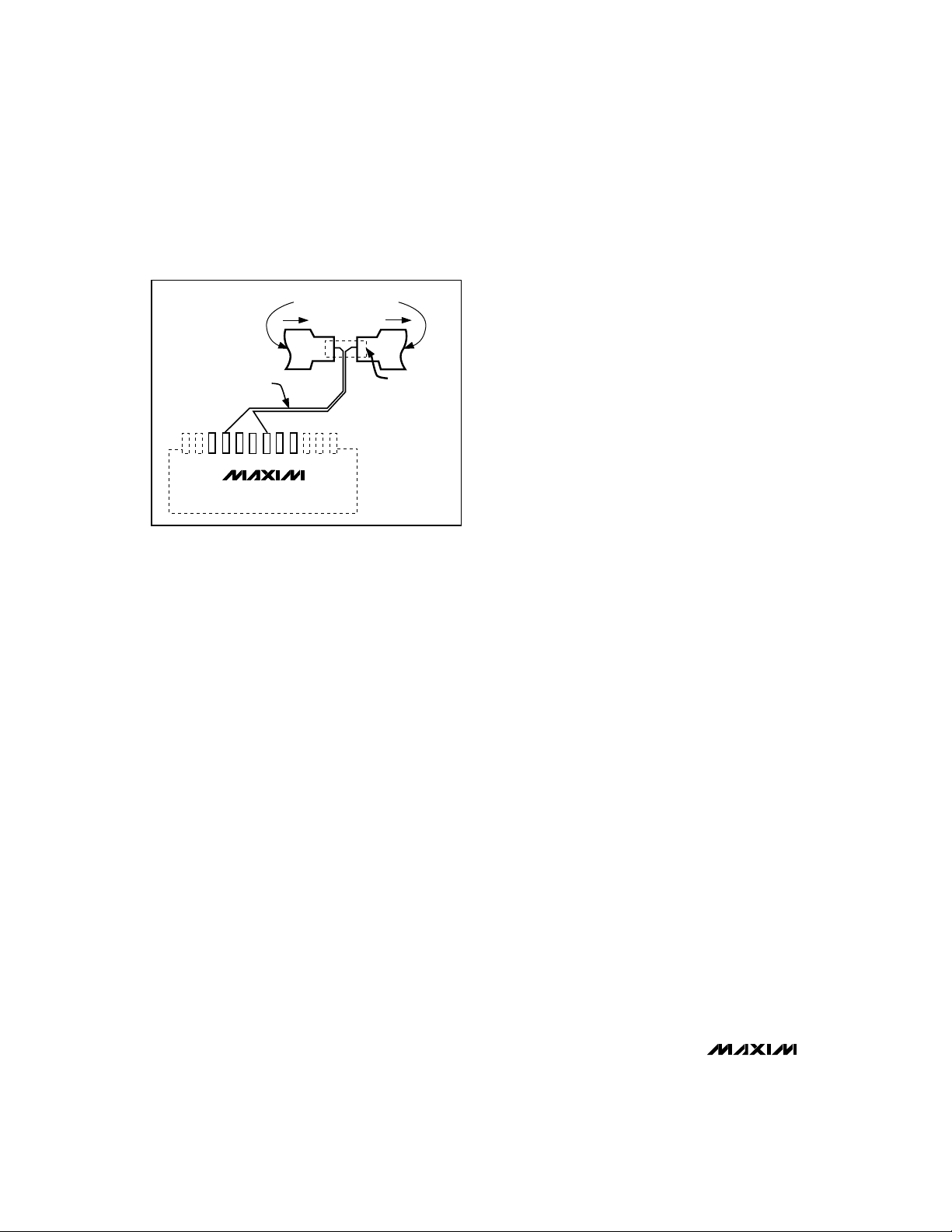
FAT, HIGH-CURRENT TRACES
MAIN CURRENT PATH
MAX783
KELVIN SENSE TRACES
MAX783
Figure 5. Kelvin Connections for the Current-Sense Resistors
SENSE RESISTOR
Ensure the transformer secondary is connected with the
right polarity: A VDD supply will be generated with either
polarity, but proper operation is possible only with the correct polarity. Test for correct connection by observing the
phase relationship between the LX3 switching node and
the transformer secondary under load. The two waveforms must be 180° out of phase.
Current-Sense Resistors (R1, R2)
The sense resistors must carry the peak current in the
inductor, which exceeds the full DC load current.
The internal current limiting starts when the voltage
across the sense resistors exceeds 100mV nominally,
80mV minimum. Use the minimum value to ensure
adequate output current capability: For the +5V supply, R1 = 80mV / (1.15 x I
R2 = 80mV/(1.15 x I
TOTAL
); for the +3.3V supply,
OUT
), assuming that LIR = 0.3.
Since the sense resistance values (e.g., R1 = 25mΩ for
I
= 3A) are similar to a few centimeters of narrow
OUT
traces on a printed circuit board, trace resistance can
contribute significant errors. To prevent this, Kelvin
connect the CS_ and FB_ pins to the sense resistors;
use separate traces not carrying any of the inductor or
load current, as shown in Figure 5. Run these traces
parallel at minimum spacing from one another. The
wiring layout for these traces is critical for stable, lowripple outputs (see the
Layout and Grounding
section).
MOSFET Switches (N1-N4)
The four N-channel power MOSFETs are usually identical and must be “logic-level” FETs; that is, they must be
fully on (have low r
drive voltage. The MOSFET r
) with only 4V gate-source
DS(ON)
should ideally be
DS(ON)
with even lower r
which increases switching time and transition losses.
DS(ON)
MOSFETs with low gate-threshold voltage specifications (i.e., maximum V
preferred, especially for high-current (5A) applications.
Output Filter Capacitors (C3–C6)
The output filter capacitors determine the loop stability
and output ripple voltage. To ensure stability, the minimum capacitance and maximum ESR values are:
CF> —————————————
(V
) (RCS) (2) (π) (GBWP)
OUT
and,
(V
ESRCF< ——————
OUT
where: CF= output filter capacitance, C6 or C7 (F)
= reference voltage, 3.3V
V
REF
= output voltage, 3.3V or 5V
V
OUT
= sense resistor (Ω)
R
CS
GBWP = gain-bandwidth product, 60kHz
= output filter capacitor ESR (Ω).
ESR
CF
Be sure to select output capacitors that satisfy both the
minimum capacitance and maximum ESR requirements. To achieve the low ESR required, it may be
appropriate to use a capacitance value 2 or 3 times
larger than the calculated minimum.
The output ripple in continuous-current mode is:
V
OUT(RPL)
= (I
) [(ESRCF+1/(2 x π x f x CF)].
LPP(MAX)
In idle-mode, the ripple has a capacitive and resistive
component:
V
(C) = ——————— x
OUT(RPL)
1 1
——— + ————— ) Volts
(
V
V
OUT(RPL)
The total ripple, V
lows:
if V
then V
otherwise, V
VIN- V
OUT
(R) = ——————- Volts
OUT(RPL)
OUT(RPL)
OUT(RPL)
OUT(RPL)
V
OUT(RPL)
have higher gate capacitance,
= 2V rather than 3V) are
GS(TH)
V
REF
) (RCS)
V
REF
(4 x 10⁻⁴) (L)
2
(R
) (CF)
CS
OUT
(0.02) (ESRCF)
R
CS
, can be approximated as fol-
(R) < 0.5 V
= V
OUT(RPL)
= 0.5 V
OUT(RPL)
(R).
OUT(RPL)
(C),
(C) +
(C),
16 _______________________________________________________________________________________
Page 17

Triple-Output Power-Supply Controller
for Notebook Computers
The voltage rating of D3 should be at least 4 x VIN+
Diode D3
5V plus a safety margin. A rating of at least 100V is
necessary for the maximum 20V supply. Use a highspeed silicon diode (with a higher breakdown voltage
and low capacitance) rather than a Schottky diode.
D3’s current rating should exceed twice the maximum
current load on VDD.
Diodes D2 and D5
Use 1N5819s or similar Schottky diodes. D2 and D5
conduct only about 3% of the time, so the 1N5819’s 1A
current rating is conservative. The voltage rating of D2
and D5 must exceed the maximum input supply voltage from the battery. These diodes must be Schottky
diodes to prevent the lossy MOSFET body diodes from
turning on, and they must be placed physically close to
their associated synchronous rectifier MOSFETs.
Soft-Start Capacitors (C13, C14)
A capacitor connected from GND to either SS pin causes that supply to ramp up slowly. The ramp time to full
current limit, tSS, is approximately 1ms for every nF of
capacitance on SS_, with a minimum value of 10µs.
Typical capacitor values are in the 10nF to 100nF range.
Because this ramp is applied to the current-limit circuit,
the actual time for the output voltage to ramp up
depends on the load current and output capacitor
value. Using Figure 1’s circuit with a 2A load and no
SS capacitor, full output voltage is reached in less than
1ms after ON_ is driven high.
Bypass Capacitors
Input Filter Capacitors (C1, C2)
Use at least 3µF/W of output power for the input filter
capacitors, C1 and C2. They should have less than
150mΩ ESR, and should be located no further than
10mm from N1 and N2 to prevent ringing. Connect the
negative terminals directly to PGND. Be careful not to
exceed the surge current ratings of the bypass capacitors. If the battery pack or AC adapter has very low
output impedance, tantalum capacitors may be damaged when initial connection is made. In this situation,
electrolytic capacitors such as Sanyo OS-CON may be
necessary. Also, take care that the RMS input current
of the MAX783 circuit does not exceed the bypass
capacitor ripple current rating. The RMS input current
(I
) can be calculated as shown below:
RMS
IRMS = RMS AC input current
= I
LOAD
————————
√V
OUT(VIN
———————–——
- V
)
OUT
V
IN
)(
Low-Voltage Operation
Low input voltages, such as the 6V end-of-life voltage
of a 6-cell NiCd battery, place extra demands on the
+5V buck regulator because of the very low input-output differential voltage. The standard application circuit works well with supply voltages down to 6V; at
input voltages less than 6V, the +5V filter capacitor
values must be increased. If the minimum battery
voltage is 6.5V or higher, the 660µF total 5V filter
capacitance can be reduced to 330µF.
The +5V supply’s load-transient response is
impaired due to reduced inductor-current slew rate,
which is in turn caused by reduced voltage applied
across the buck inductor during the high-side
switch-on time. So, the +5V output sags when hit
with an abrupt load current change, unless the +5V
filter capacitor value is increased. Only the capacitance is affected and ESR requirements don’t
change. Therefore, the added capacitance can be
supplied by an additional low-cost bulk capacitor in
parallel with the normal low-ESR switching-regulator
capacitor. The equation for voltage sag under a
step-load change follows:
2
(I
)(L)
V
= —————————————————
SAG
where DMAX is the maximum duty cycle. Higher duty
cycles are possible when the oscillator frequency is
reduced to 200kHz, due to fixed propagation delays
through the PWM comparator becoming a lesser part of
the whole period. The tested worst-case limit for DMAX
is 92% at 200kHz. Lower inductance values can reduce
the filter capacitance requirement, but only at the
expense of increased noise at high input voltages
(resulting from higher peak currents).
(2)(CF) (V
STEP
IN(MIN)
x DMAX - V
OUT
)
MAX783
______________________________________________________________________________________ 17
Page 18

Triple-Output Power-Supply Controller
for Notebook Computers
Good layout is necessary to achieve the designed out-
Layout and Grounding
put power, high efficiency, and low noise. Good layout
includes use of a ground plane, appropriate component placement, and correct routing of traces using
appropriate trace widths. The following points are in
order of importance:
1. A ground plane is essential for optimum performance.
MAX783
In most applications, the power supply is located on a
multilayer motherboard, and full use of the four or
more copper layers is recommended. Use the top
and bottom layers for interconnections, and the inner
layers for an uninterrupted ground plane.
2. Keep the Kelvin-connected current-sense traces
short, close together, and away from switching
nodes. See Figure 5. Important: Place the currentsense resistors close to the IC (less than 10mm
away if possible).
3. Place the LX node components N1, N2, D2, and L1
as close together as possible. This reduces resistive
and switching losses and keeps noise due to
ground inductance confined. Do the same with the
other LX node components N3, N4, D5, and L2.
4. The input filter capacitor C1 should be less than
10mm away from N1’s drain. The connecting copper trace carries large currents and must be at least
2mm wide, preferably 5mm.
Similarly, place C2 close to N3’s drain, and connect
them with a wide trace.
5. Keep the gate connections to the MOSFETs short for
low inductance (less than 20mm long and more than
0.5mm wide) to ensure clean switching.
6. To achieve good shielding, it is best to keep all
high-voltage switching signals (MOSFET gate drives DH3 and DH5, BST3 and BST5, and the two LX
nodes) on one side of the board and all sensitive
nodes (CS3, CS5, FB3, FB5 and REF) on the other
side.
7. Connect the GND and PGND pins directly to the
ground plane, which should ideally be an inner layer
of a multilayer board.
8. Connect the bypass capacitor C7 very close (less
than 10mm) to the VL pin.
9. Minimize the capacitance at the transformer secondary. Place D3 and C12 very close to each other
and to the secondary, then route the output to the
IC’s VDD pin with a short trace. Bypass with 0.1µF
close to the VDD pin if this trace is longer than
50mm.
The layout for the evaluation board is shown in the
Evaluation Kit
noise, high-efficiency example.
section. It provides an effective, low-
18 ______________________________________________________________________________________
Page 19
Triple-Output Power-Supply Controller
for Notebook Computers
Table 3. Surface-Mount Components
(See Figure 1 for schematic and Table 4 for manufacturers' telephone numbers.)
COMPONENT TYPE MANUFACTURER PART NUMBER
C1, C2
C3, C4
C5, C6
C7 4.7µF 16V tantalum Sprague 595D475X0016A
C8, C9, C15 1µF, 20V tantalum Sprague 595D105X0020T
C10, C11 0.1µF, 16V tantalum Murata-Erie GRM42-6X7R104K50V
C12 2.2µF, 25V tantalum Sprague 595D225X0025B
C13, C14 0.01µF, ceramic Murata-Erie GRM42-6X7R103K50V
D1 Dual low-power Schottky Central Semiconductor CMPSH-3A
D3 Fast silicon rectifier Nihon EC11FS1
D2, D5 1N5819 Schottky Nihon EC10QS04
D6 18V, 100mW zener diode Central Semiconductor CMPZ5248
R1 0.025Ω SMT resistor IRC LR2010-01-R025-F
R2 0.02Ω SMT resistor IRC LR2010-01-R020-F
N1-N4 N-channel MOSFETs International Rectifier IRF7101 (Note 1)
L1 10µH, 2.5A inductor Sumida CDR125-100
L2 10µH, 1:4 transformer (Note 2)
Note 1: Four IRF7101s total; each device has both sections connected in parallel.
Note 2: These transformers have different sizes and pinouts. The MAX783 EV kit has the correct pad layout for the TTI5902 trans-
former, but all the transformers listed can be wired in easily.
33µF, 35V tantalum Sprague 595D336X0035R2B
33µF, 25V tantalum
330µF, 10V tantalum Sprague 595DD337X0010R2B
330µF, 6.3V tantalum AVX TPSE337M006R0100
150µF, 10V tantalum Sprague 595D157X0010D2B
220µF, 10V tantalum AVX TPSE227M010R0100
AVX TPSE336M025R0300
Transpower TTI5897 (for 3.3V at 1A)
Transpower TTI5902 (for 3.3V at 3A)
Coiltronics CTX03-12210 (for 3.3V at 2A)
Table 4. Surface-Mount Component Suppliers
Company USA Phone
Factory Fax
[country code]
MAX783
AVX
Central Semi
Coiltronics
International Rectifier
IRC
Murata-Erie
Nihon
Sprague
Sumida
Transpower Tech.
*Distributor
[ 1 ] 207-283-1941
[ 1 ] 516-435-1824
[ 1 ] 407-241-9339
[ 1 ] 310-322-3332
[ 1 ] 512-992-3377
[ 1 ] 404-736-3030
[81] 3-3494-7414
[ 1 ] 508-339-5063
[81] 3-3607-5428
[ 1 ] 702-831-3521
______________________________________________________________________________________ 19
(207) 282-5111
(800) 282-4975
(516) 435-1110
(407) 241-7876
(310) 322-3331
(512) 992-7900
(404) 736-1300
(805) 867-2555*
(508) 339-8900
(708) 956-0666
(702) 831-0140
Page 20

Triple-Output Power-Supply Controller
for Notebook Computers
______________________________________________
___________EV Kit Standard Features
♦ Battery Range: 5.5V to 20V*
♦ Load Capability: 5V at 3A*
MAX783
♦ 3.3V and 5V Keep-Alive Linear Regulator Outputs
♦ Dual PCMCIA VPP Outputs
♦ Oscillator Sync Input
For wider input voltage range or higher load current,
*
see the Design Procedure.
3.3V at 3A*
12V at 120mA or
15V at 200mA
_________________EV Kit Description
The MAX783 evaluation kit (EV kit) is a preassembled
and tested demonstration board that embodies the
standard application circuit, with some extra pull-up
and pull-down resistors needed to set default logic signal levels. The board comes configured to accept battery voltages between 5.5V and 20V, but it can be
reconfigured for voltages between 5.5V and 30V. The
maximum voltage for safe operation (20V) is determined by the breakdown voltage rating of the external
MOSFETs and input filter capacitor (C1 and C2) voltage ratings; if these are replaced with high-voltage
devices, the board can tolerate 30V input without damage (36V absolute max).
Load current capability of the standard board is 3A at
each main output (5V and 3.3V) and 60mA at each 12V
VPP output. Load current capability can also be configured by selecting appropriate external components
and sense resistor values, with practical load capability
up to 7A at each main output and 500mA on the 15V
flyback output (see the
uring both load and input voltage capability). All functions are controlled by two on-board dipswitches,
which can be overridden by external CMOS/TTL logic
signals if desired (provided the dipswitches are set to
off first).
See Table 3 for the EV kit components. These components correspond exactly to Figure 1's Standard
Application Circuit, with the addition of the following
chip resistors (which are required only to set default
logic and supply levels). The comparator outputs both
swing 0V to 5V unless R14 is removed and R12 is
installed, in which case their output swing is 0V to 15V.
R3-R11 1MΩ 5% resistors (logic pull-down, usually not
needed and not installed in normal applications)
Design Procedure
for reconfig-
Evaluation Kit Information
R12 Open-circuit (no resistor installed)
R13 100kΩ 5% chip resistor (SYNC pull-down,
R14 560Ω 5% resistor (pull-up for comparator sup-
Connect a stiff (30W or better) bench power supply to the
+VINand GND pads found on the edge of the board.
Turn up the input voltage to somewhere between 5V and
20V. Set switches SW2A, SW2B, and SW2C on (if they
are not already on), taking the device out of shutdown
and turning on the main switching regulators. Set switch
SW2D off so that the oscillator is set to 200kHz, which is
the appropriate frequency for the 6V-20V input range.
The main outputs are now regulating and ready for heavy
loads. For best output accuracy and noise characteristics, loads should be returned separately to the GND
pad corresponding to and adjacent to each output
(+3OUT and +5OUT). Normal full-load regulation
error is typically -2.5% while keeping the outputs within tolerance. If the measured error is higher, there may
be drops in the wiring or ground. Ensure the voltmeter
is sensing directly at the output and ground pads.
To observe normal PWM switching action, place a 1A
load on either output and observe the corresponding
switching node (device LX_ pin) while varying the input
voltage. Without a load, the switching waveforms are
intermittent and difficult to trigger on and it may appear
that the board isn’t working (except for the presence of
output voltage).
To exercise the VPP controls, first ensure the 3.3V
switch-mode supply is ON. The loosely regulated flyback voltage (13V to 19V) will be present at the edge
pad marked “+15OUT”. Turn on each VPP output by
setting the appropriate code on SW1, where ON = HIGH
(see Table 1).
The 5V linear regulator output is always present, even in
shutdown mode, and can be measured at the VL pad. If
the battery is connected and VL is not at 5V or close to it,
something is wrong (excess VL load, possibly). The precision 3.3V linear regulator (REF) is activated by taking the
device out of shutdown mode (by turning SW2C on).
Turning on the SW2D sets the oscillator to 300kHz, but
the external component values should be changed first
(see the
chronized to an external clock signal by driving the
SYNC pad with a 240kHz to 350kHz pulse train of 5V
amplitude while SW2D is off.
usually shorted out)
ply, usually shorted out or left open)
___________EV Kit Quick Reference
Design Procedure
). The oscillator can be syn-
20 ______________________________________________________________________________________
Page 21
Triple-Output Power-Supply Controller
for Notebook Computers
MAX783
VPPA
VL
VPPB
+15OUT
+3.3OUT
C6
C5
Q1
VH
RDY5
150µF
150µF
SYNC
Q2
REF
D6
18V
R2
20mΩ
D1B
C12
D3
31
BST3
L2
2.2µF
N3
C11
33
DH3
D5
10µH
N4
0.1µF
32
30
35
LX3
DL3
CS3
MAX783
BST5
DH5
LX5
DL5
24
D1A
R6
R5R4
R3
23
22
C10
0.1µF
N1
L1
10µH
R1
25mΩ
C4
330µF
C3
330µF
+5OUT
CS5
25
21
N2
D2
C2
33µF
C7
4.7µF
C8
1µF
C9
1µF
11
VPPB
10
VDD
DB0
DB1
18
17
DB0
DB1
9
28
VPPA
29
V+ VL
DA0
DA1
16
15
C1
33µF
BC D
A
SW1
IN
+V
DA1
DA0
34
FB3
FB5
27
R14
TO VL
R12
C14
0.01µF
36
SS3
SS5
20
C13
0.01µF
BC
A
560Ω
OPEN
5VH8
ON31ON519SHDN2D1
SW2
ON3
RDY5
ON5
7
6
Q1
3
SHDN
SW2D
R13
100k
C15
13
R11R10
R8
1µF
REF
1226
PGND GND
R9
R3 - R11 = 1MΩ
R7
14
Q2
SYNC
D2
4
D1
D2
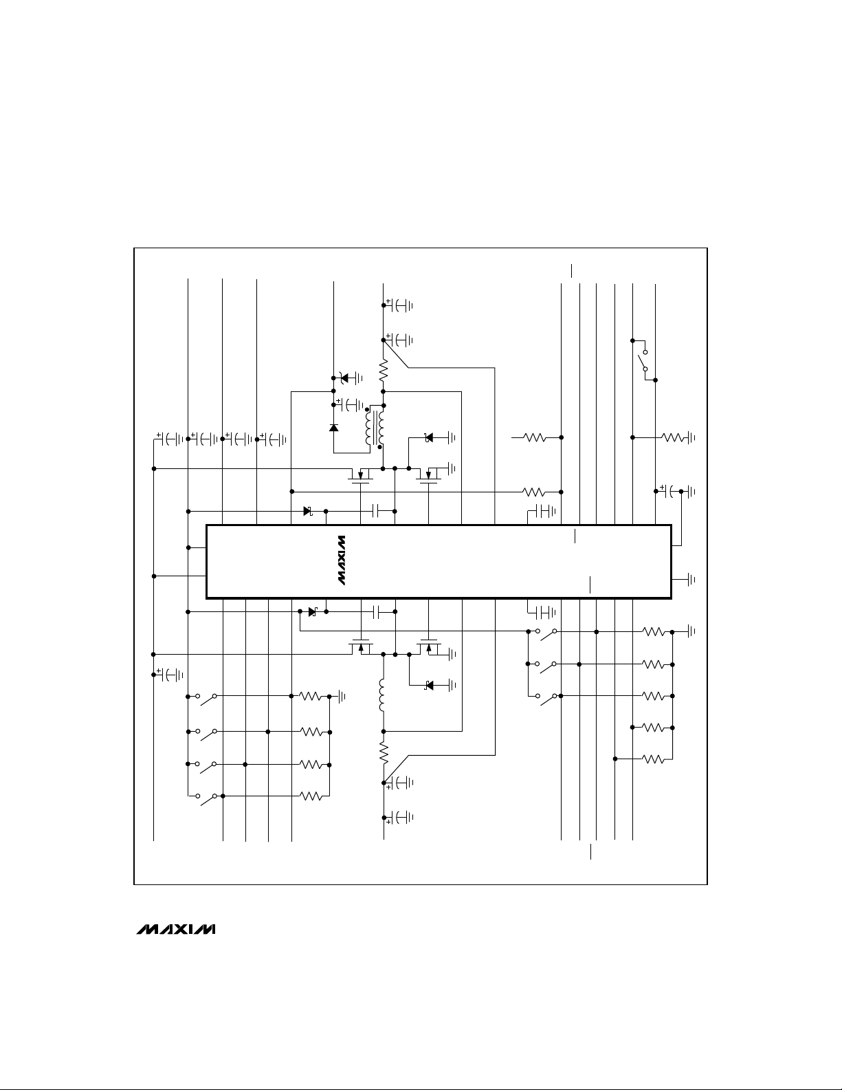
Figure 6. MAX783 EV Kit Schematic
______________________________________________________________________________________ 21
Page 22
Triple-Output Power-Supply Controller
for Notebook Computers
MAX783
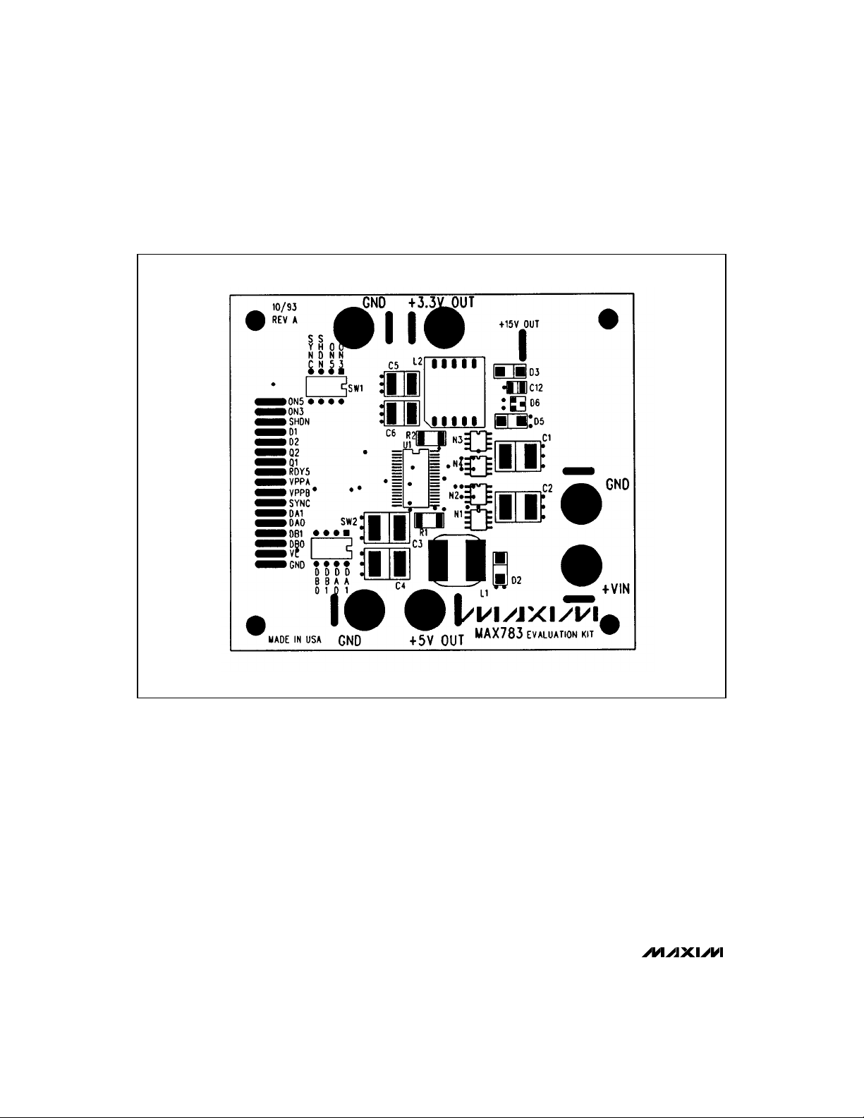
Figure 7. MAX783 EV Kit Top Component Layout and Silk Screen, Top View
22 ______________________________________________________________________________________
Page 23
Triple-Output Power-Supply Controller
for Notebook Computers
MAX783
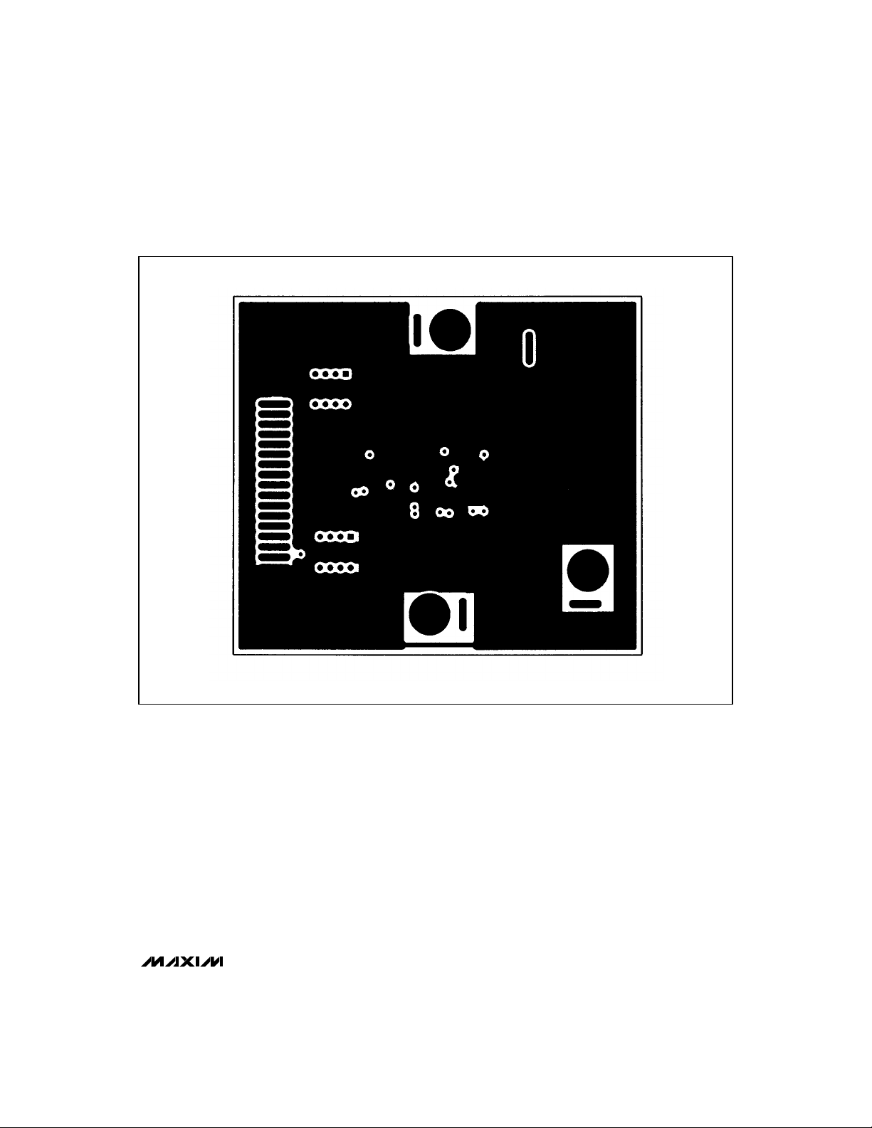
Figure 8. MAX783 EV Kit Ground Plane (Layers 2 and 3), Top View
______________________________________________________________________________________ 23
Page 24
Triple-Output Power-Supply Controller
for Notebook Computers
MAX783
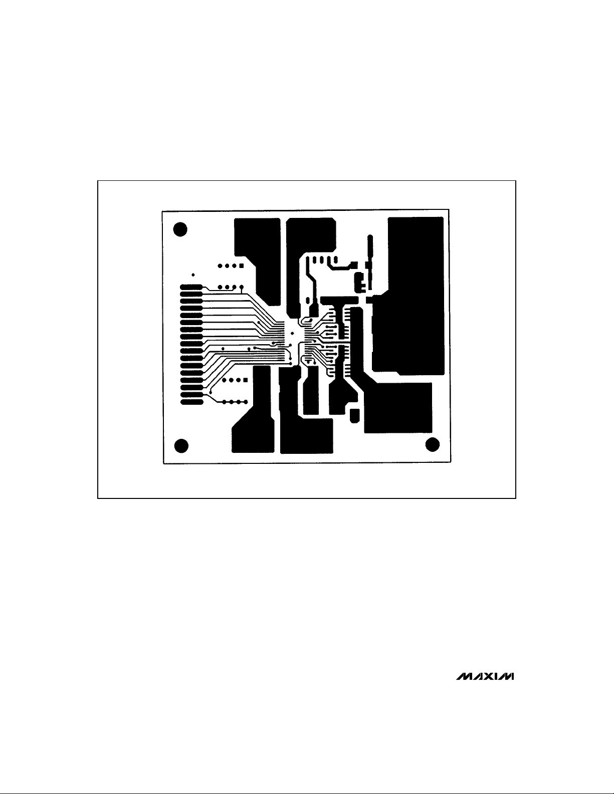
Figure 9. MAX783 EV Kit Top Layer (Layer 1), Top View
24 ______________________________________________________________________________________
Page 25
Triple-Output Power-Supply Controller
for Notebook Computers
MAX783
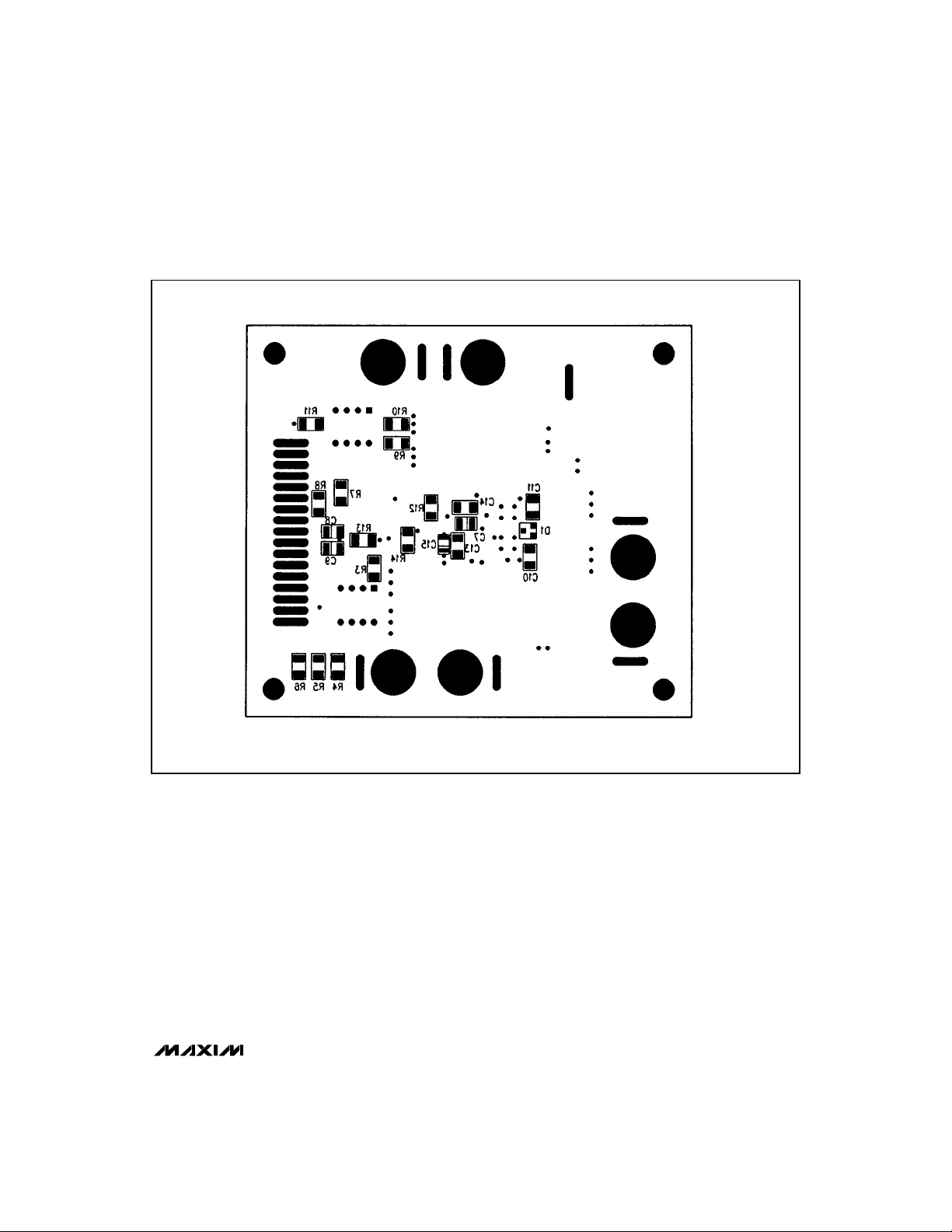
Figure 10. MAX783 EV Kit, Bottom Component Layout and Silk Screen, Bottom View
______________________________________________________________________________________ 25
Page 26

Triple-Output Power-Supply Controller
for Notebook Computers
MAX783
Figure 11. MAX783 EV Kit, Bottom Layer (Layer 4), Top View
26 ______________________________________________________________________________________
Page 27

Triple-Output Power-Supply Controller
for Notebook Computers
MAX783
Figure 12. MAX783 EV Kit, Drill Schedule
______________________________________________________________________________________ 27
Page 28

Triple-Output Power-Supply Controller
for Notebook Computers
___________________Chip Topography _Ordering Information (continued)
FB3
SS3
SHDN
D2
DH3
CS3
ON3
D1
VH
Q2
Q1
MAX783
RDY5
VPPA
VPPB
SYNC
VDD
GND
REF
DA1
DA0
DB1
DB0
SS5 DH5
ON5
0.132"
(3.353mm)
CS5
LX3
BST3
DL3
V+
VL
FB5
PGND
DL5
BST5
LX5
0.181"
(4.597mm)
TRANSISTOR COUNT: 1569
SUBSTRATE CONNECTED TO GND
________________________________________________________Package Information
HE
PART TEMP. RANGE PIN-PACKAGE
MAX783SCBX 0°C to +70°C 36 SSOP
MAX783C/D 0°C to +70°C Dice*
MAX783EBX -40°C to +85°C 36 SSOP
MAX783REBX -40°C to +85°C 36 SSOP
MAX783SEBX -40°C to +85°C 36 SSOP
EV KIT TEMP. RANGE BOARD TYPE
0°C to +70°C Surface MountMAX783EVKIT-SO
* Dice are specified at +25°C only.
INCHES MILLIMETERS
DIM
A
A1
B
C
D
E
e
H
L
α
MIN
0.094
0.004
0.011
0.009
0.604
0.292
0.398
0.020
0˚
MAX
MIN
0.104
2.39
0.011
0.10
0.017
0.30
0.012
0.23
0.610
15.34
0.298
7.42
0.80 BSC0.032 BSC
0.416
0.035
10.10
0.51
8˚
0˚
MAX
2.64
0.28
0.44
0.32
15.49
7.57
10.57
0.89
21-0032A
V
OUT
3.6V
—
3.3V
3.45V
3.6V
8˚
D
α
A
0.127mm
A1
e
B
0.004in.
C
L
36-PIN PLASTIC
SHRINK
SMALL-OUTLINE
PACKAGE
Maxim cannot assume responsibility for use of any circuitry other than circuitry entirely embodied in a Maxim product. No circuit patent licenses are
implied. Maxim reserves the right to change the circuitry and specifications without notice at any time.
28
__________________Maxim Integrated Products, 120 San Gabriel Drive, Sunnyvale, CA 94086 (408) 737-7600
© 1994 Maxim Integrated Products Printed USA is a registered trademark of Maxim Integrated Products.
 Loading...