

Page 1
19-0146; Rev 2; 5/94
Evaluation Kit
Information Included
Controller for Notebook Computers
_______________General Description
The MAX782 is a system-engineered power-supply controller for notebook computers or similar battery-powered
equipment. It provides two high-performance step-down
(buck) pulse-width modulators (PWMs) for +3.3V and +5V,
and dual PCMCIA VPP outputs powered by an integral flyback winding controller. Other functions include dual, lowdropout, micropower linear regulators for CMOS/RTC backup, and three precision low-battery-detection comparators.
High efficiency (95% at 2A; greater than 80% at loads
from 5mA to 3A) is achieved through synchronous rectification and PWM operation at heavy loads, and IdleModeTMoperation at light loads. It uses physically
small components, thanks to high operating frequencies (300kHz/200kHz) and a new current-mode PWM
architecture that allows for output filter capacitors as
small as 30µF per ampere of load. Line- and load-transient response are terrific, with a high 60kHz unity-gain
crossover frequency allowing output transients to be
corrected within four or five clock cycles. Low system
cost is achieved through a high level of integration and
the use of low-cost, external N-channel MOSFETs. The
integral flyback winding controller provides a low-cost,
+15V high-side output that regulates even in the
absence of a load on the main output.
Triple-Output Power-Supply
___________________________Features
♦ Dual PWM Buck Controllers (+3.3V and +5V)
♦ Dual PCMCIA VPP Outputs (0V/5V/12V)
♦ Three Precision Comparators or Level Translators
♦ 95% Efficiency
♦ 420µA Quiescent Current;
70µA in Standby (linear regulators alive)
♦ 5.5V to 30V Input Range
♦ Small SSOP Package
♦ Fixed Output Voltages Available:
3.3 (standard)
3.45 (High-Speed Pentium™)
3.6 (PowerPC™)
______________Ordering Information
PART TEMP. RANGE PIN-PACKAGE
MAX782CBX 0°C to +70°C 36 SSOP
MAX782RCBX 0°C to +70°C 36 SSOP
MAX782SCBX 0°C to +70°C 36 SSOP
Ordering Information continued on last page.
__________________Pin Configuration
TOP VIEW
Other features include low-noise, fixed-frequency PWM
operation at moderate to heavy loads and a synchronizable oscillator for noise-sensitive applications such as
electromagnetic pen-based systems and communicating computers. The MAX782 is a monolithic BiCMOS IC
available in fine-pitch, SSOP surface-mount packages.
_______________________Applications
Notebook Computers
Portable Data Terminals
Communicating Computers
Pen-Entry Systems
______Typical Application Diagram
+3.3V
+5V
µP
MEMORY
PERIPHERALS
DUAL
PCMCIA
SLOTS
5.5V
TO
30V
VPP
CONTROL
ON3
ON5
SYNC
Idle-Mode is a trademark of Maxim Integrated Products. Pentium is a trademark of Intel
™
MAX782
4
POWER
SECTION
SUSPEND POWER
LOW-BATTERY WARNING
VPP (0V/5V/12V)
VPP (0V/5V/12V)
ON3
1
D1
2
D2
3
D3
4
VH
5
Q3
Q2
Q1
VPPA
VDD
VPPB
GND
REF
SYNC
DA1
DA0
DB1
DB0
MAX782
6
7
8
9
10
11
12
13
14
15
16
17
18
SSOP
.
PowerPC is a trademark of IBM.
MAX782
V
OUT
3.3V
3.45V
3.6V
36
SS3
CS3
35
FB3
34
DH3
33
LX3
32
31
BST3
30
DL3
29
V+
28
VL
27
FB5
26
PGND
25
DL5
24
BST5
23
LX5
22
DH5
21
CS5
20
SS5
19
ON5
________________________________________________________________
Maxim Integrated Products
Call toll free 1-800-998-8800 for free samples or literature.
1
Page 2
Triple-Output Power-Supply
Controller for Notebook Computers
ABSOLUTE MAXIMUM RATINGS
V+ to GND.................................................................-0.3V, +36V
PGND to GND........................................................................±2V
VL to GND ...................................................................-0.3V, +7V
BST3, BST5 to GND ..................................................-0.3V, +36V
LX3 to BST3.................................................................-7V, +0.3V
LX5 to BST5.................................................................-7V, +0.3V
Inputs/Outputs to GND
MAX782
(D1-D3, ON5, REF, SYNC, DA1, DA0, DB1, DB0, ON5,
SS5, CS5, FB5, CS3, FB3, SS3, ON3)..........-0.3V, (VL + 0.3V)
VDD to GND.................................................................-0.3V, 20V
VPPA, VPPB to GND.....................................-0.3V, (VDD + 0.3V)
VH to GND...................................................................-0.3V, 20V
Q1-Q3 to GND.................................................-0.3V, (VH + 0.3V)
DL3, DL5 to PGND...........................................-0.3V, (VL + 0.3V)
Stresses beyond those listed under “Absolute Maximum Ratings‘” may cause permanent damage to the device. These are stress ratings only, and functional
operation of the device at these or any other conditions beyond those indicated in the operational sections of the specifications is not implied. Exposure to
absolute maximum rating conditions for extended periods may affect device reliability.
ELECTRICAL CHARACTERISTICS
(V+ = 15V, GND = PGND = 0V, IVL= I
unless otherwise noted.)
PARAMETER CONDITIONS MIN TYP MAX UNITS
+3.3V AND 5V STEP-DOWN CONTROLLERS
Input Supply Range 5.5 30 V
FB5 Output Voltage 4.80 5.08 5.20 V
FB3 Output Voltage
Load Regulation Either controller (CS_ - FB_ = 0mV to 70mV) 2 %
Line Regulation Either controller (V+ = 6V to 30V) 0.03 %/V
Current-Limit Voltage
SS3/SS5 Source Current 2.5 4.0 6.5 µA
SS3/SS5 Fault Sink Current 2 mA
15V FLYBACK CONTROLLER
VDD Regulation Setpoint Falling edge, hysteresis = 1% V
VDD Shunt Setpoint Rising edge, hysteresis = 1% V
VDD Shunt Current VDD = 20V 23 mA
Quiescent VDD Current 140 300 µA
VDD Off Current 15 30 µA
PCMCIA REGULATORS (Note 1)
VPPA/VPPB Output Voltage
VPPA/VPPB Off Input Current Program to Hi-Z, VDD = 19V, 0V < VPP < 12V 35 µA
= 0mA, ON3 = ON5 = 5V, other digital input levels are 0V or +5V, TA = T
REF
0mV < (CS5-FB5) < 70mV, 6V < V+ < 30V
(includes load and line regulation)
0mV < (CS3-FB3) < 70mV, 6V < V+ < 30V
(includes load and line regulation)
CS3-FB3 or CS5-FB5
CS5-FB5 (VDD < 13V, flyback mode) -50 -100 -160
VDD = 18V, ON3 = ON5 = 5V,
VPPA/B programmed to 12V with no external load
VDD = 18V, ON3 = ON5 = 5V,
VPPA/B programmed to Hi-Z or 0V
Program to 12V, 13V < VDD < 19V, 0mA < IL< 60mA 11.6 12.1 12.5
Program to 5V, 13V < VDD < 19V, 0mA < IL< 60mA 4.85 5.05 5.20
Program to 0V, 13V < VDD < 19V, -0.3mA < IL< 0.3mA -0.3 0.3
DH3 to LX3..................................................-0.3V, (BST3 + 0.3V)
DH5 to LX5..................................................-0.3V, (BST5 + 0.3V)
REF, VL, VPP Short to GND........................................Momentary
REF Current.........................................................................20mA
VL Current...........................................................................50mA
VPPA, VPPB Current.........................................................100mA
Continuous Power Dissipation (T
SSOP (derate 11.76mW/°C above +70°C) ...................941mW
Operating Temperature Ranges:
MAX782CBX/MAX782__CBX...............................0°C to +70°C
MAX782EBX/MAX782__EBX ............................-40°C to +85°C
Storage Temperature Range.............................-65°C to +160°C
Lead Temperature (soldering, 10sec).............................+300°C
MAX782
MAX782R
MAX782S
= +70°C)
A
3.17 3.35 3.46
3.32 3.50 3.60
3.46 3.65 3.75
80 100 120
13 14
18 20
MIN
to T
mV
V
V
V
V
MAX
,
2 _______________________________________________________________________________________
Page 3
Triple-Output Power-Supply
Controller for Notebook Computers
ELECTRICAL CHARACTERISTICS (continued)
(V+ = 15V, GND = PGND = 0V, IVL= I
unless otherwise noted.)
PARAMETER CONDITIONS MIN TYP MAX UNITS
INTERNAL REGULATOR AND REFERENCE
VL Output Voltage
VL Fault Lockout Voltage
VL/FB5 Switchover Voltage Rising edge of FB5, hysteresis = 1% 4.2 4.7 V
REF Output Voltage No external load (Note 2) 3.24 3.36 V
REF Fault Lockout Voltage Falling edge 2.4 3.2
REF Load Regulation 0mA < IL< 5mA 30 75 mV
V+ Standby Current 70 110 µA
Quiescent Power Consumption
(both PWM controllers on)
V+ Off Current
COMPARATORS
D1-D3 Trip Voltage Falling edge, hysteresis = 1%
D1-D3 Input Current D1 = D2 = D3 = 0V to 5V
Q1-Q3 Source Current VH = 15V, Q1-Q3 forced to 2.5V 12 20 30 µA
Q1-Q3 Sink Current
Q1-Q3 Output High Voltage
Q1-Q3 Output Low Voltage
Quiescent VH Current VH = 18V, D1 = D2 = D3 = 5V, no external load
OSCILLATOR AND INPUTS/OUTPUTS
Oscillator Frequency
SYNC High Pulse Width 200 ns
SYNC Low Pulse Width 200 ns
SYNC Rise/Fall Time Not tested 200 ns
Oscillator SYNC Range 240 350 kHz
Maximum Duty Cycle
Input Low Voltage ON3, ON5, DA0, DA1, DB0, DB1, SYNC 0.8 V
Input High Voltage
Input Current
DL3/DL5 Sink/Source Current DL3, DL5 forced to 2V 1 A
DH3/DH5 Sink/Source Current BST3-LX3 = BST5-LX5 = 4.5V, DH3, DH5 forced to 2V 1 A
DL3/DL5 On Resistance High or low 7 Ω
DH3/DH5 On Resistance High or low, BST3-LX3 = BST5-LX5 = 4.5V 7 Ω
Note 1: Output current is further limited by maximum allowable package power dissipation.
Note 2: Since the reference uses VL as its supply, V+ line regulation error is insignificant.
= 0mA, ON3 = ON5 = 5V, other digital input levels are 0V or +5V, TA = T
REF
ON5 = ON3 = 0V, 5.5V < V+ < 30V, 0mA < IL< 25mA
Falling edge, hysteresis = 1% 3.6 4.2 V
D1 = D2 = D3 = ON3 = ON5 = DA0 = DA1 = DB0 =
DB1 = 0V, V+ = 30V
D1 = D2 = D3 = DA0 = DA1 = DB0 = DB1 = 0V,
FB5 = CS5 = 5.25V, FB3 = CS3 = 3.5V
FB5 = CS5 = 5.25V, VL switched over to FB5 30 60 µA
VH = 15V, Q1-Q3 forced to 2.5V 200 500 1000 µA
I
= 5µA, VH = 3V
SOURCE
I
= 20µA, VH = 3V
SINK
SYNC = 3.3V 270 300 330
SYNC = 0V or 5V 170 200 230
SYNC = 3.3V 89 92
SYNC = 0V or 5V 92 95
ON3, ON5, DA0, DA1, DB0, DB1 2.4
SYNC VL-0.5
ON3, ON5, DA0, DA1, DB0, DB1, VIN= 0V or 5V
4.5 5.5
6.0 8.6
1.61 1.69 V
VH-0.5 V
610µA
MIN
±100
0.4 V
±1 µA
to T
V
V
mW
nA
kHz
%
V
MAX782
,
MAX
_______________________________________________________________________________________ 3
Page 4
Triple-Output Power-Supply
Controller for Notebook Computers
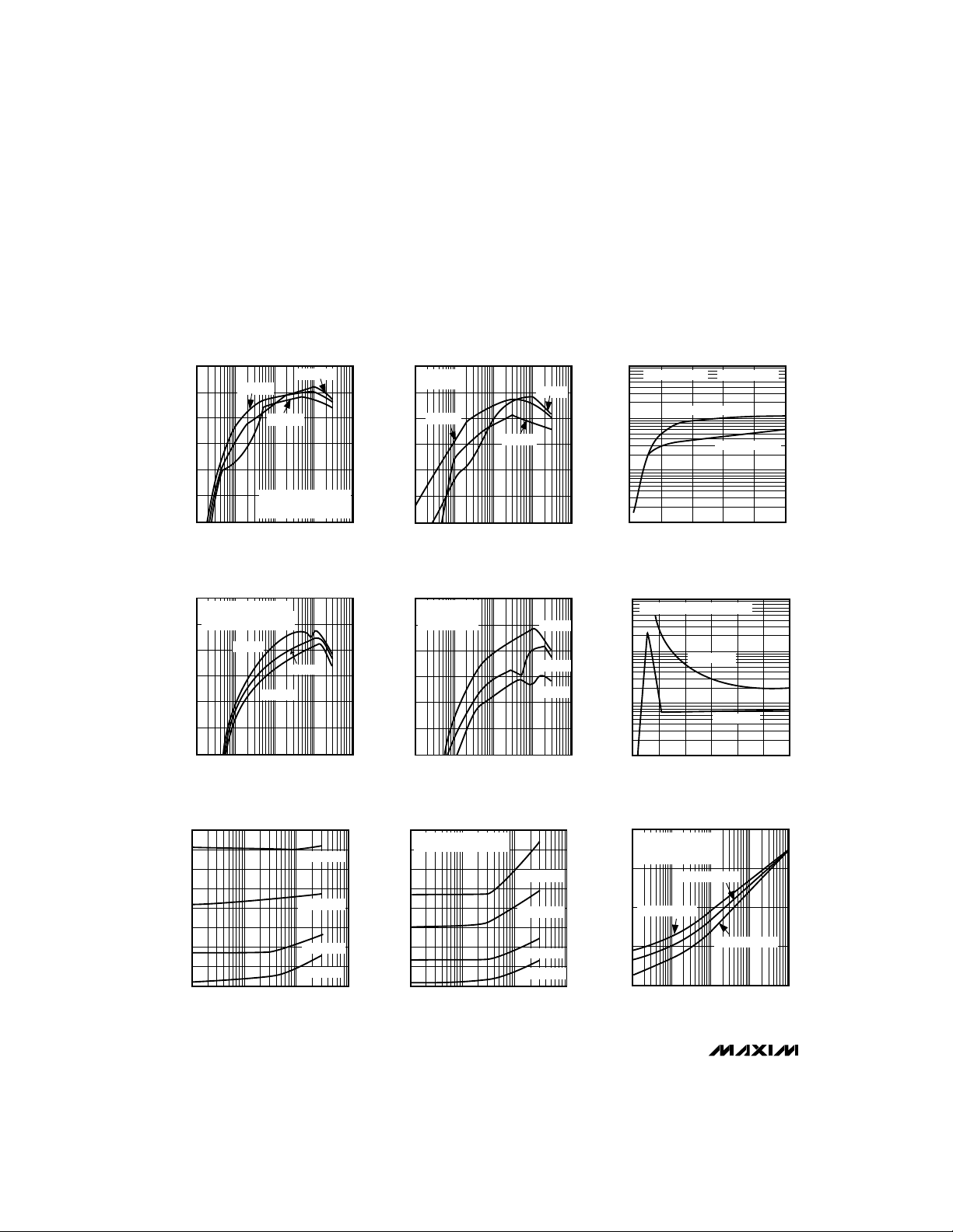
__________________________________________Typical Operating Characteristics
(Circuit of Figure 1, Transpower transformer type TTI5870, TA= +25°C, unless otherwise noted.)
+5V OUTPUT CURRENT, 200kHz
100
MAX782
90
EFFICIENCY (%)
80
70
0.001 0.1 10
0.01 1
+5V OUTPUT CURRENT (A)
+3.3V OUTPUT CURRENT, 200kHz
100
+5V ON, +5V LOAD = 0mA
IDD = 0mA,
COMPONENTS OF TABLE 5
90
EFFICIENCY (%)
80
70
0.001 0.1 10
0.01 1
+3.3V OUTPUT CURRENT (A)
+5V OUTPUT CURRENT vs.
MINIMUM INPUT VOLTAGE, 300kHz
9
8
EFFICIENCY vs.
VIN = 10V
VIN = 15V
COMPONENTS,
OF TABLE 5. SYNC = 0V,
+3.3V OFF, I
EFFICIENCY vs.
VIN = 6V
VIN = 15V
VIN = 6V
DD
VIN = 10V
IDD = 300mA
= 0mA
EFFICIENCY vs.
+5V OUTPUT CURRENT, 300kHz
100
IDD = 0mA
+3.3V OFF
VIN = 15V
90
EFFICIENCY (%)
80
70
0.001 0.01 1
+5V OUTPUT CURRENT (A)
EFFICIENCY vs.
+3.3V OUTPUT CURRENT, 300kHz
100
I
= 0mA
DD
+5V ON
+5V LOAD = 0mA
90
EFFICIENCY (%)
80
70
0.001 0.01 1
+3.3V OUTPUT CURRENT (A)
+5V OUTPUT CURRENT vs.
MINIMUM INPUT VOLTAGE, 200kHz
9
COMPONENTS OF TABLE 4,
SYNC = 0V
8
VIN = 6V
VIN = 30V
0.1 10
VIN = 6V
VIN = 15V
VIN = 30V
0.1 10
IDD = 300mA
IDD OUTPUT CURRENT vs. INPUT VOLTAGE
COILTRONIX CTX03-12062 TRANSFORMER
10
+3V LOAD = 0mA R
1
0.1
LOAD CURRENT (A)
DD
I
0.01
510 20 30
10000
1000
100
INPUT CURRENT (µA)
10
0 5 15 25
1000
100
+5V LOAD = 0A-1A
15 25
INPUT VOLTAGE (V)
QUIESCENT INPUT CURRENT vs.
INPUT VOLTAGE
+3.3V LOAD = +5V LOAD = 0mA
+5V, +3V ON
10 20 30
INPUT VOLTAGE (V)
SWITCHING FREQUENCY vs.
LOAD CURRENT
CIRCUIT OF FIGURE 1,
SYNC = REF (300kHz)
ON3 = ON5 = 5V
+5V, VIN = 7.5V
= 0.020Ω
SENSE
+5V LOAD = 3A
+5V, +3V OFF
7
6
MINIMUM INPUT VOLTAGE (V)
5
0.01 0.1 10
+5V OUTPUT CURRENT (A)
IDD = 140mA
IDD = 60mA
IDD = 0mA
1
7
6
MINIMUM INPUT VOLTAGE (V)
5
0.01 0.1 10
+5V LOAD CURRENT (A)
IDD = 140mA
I
= 60mA
DD
IDD = 0mA
1
10
+5V, VIN = 30V
1
SWITCHING FREQUENCY (kHz)
0.1
100µA 10mA 1A
1mA 100mA
LOAD CURRENT
4 _______________________________________________________________________________________
+3.3V, VIN = 7.5V
Page 5
Triple-Output Power-Supply
Controller for Notebook Computers
_____________________________Typical Operating Characteristics (continued)
(Circuit of Figure 1, Transpower transformer type TTI5870, TA= +25°C, unless otherwise noted.)
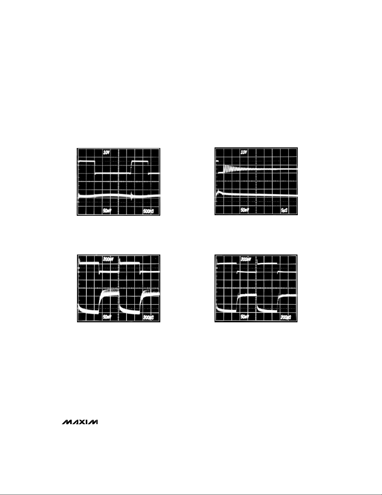
PULSE-WIDTH MODULATION MODE WAVEFORMS
HORIZONTAL = 500ns/div
+5V OUTPUT CURRENT = 1A
INPUT VOLTAGE = 16V
+5V LOAD-TRANSIENT RESPONSE
LX VOLTAGE
10V/div
+5V OUTPUT
VOLTAGE
50mV/div
3A
LOAD CURRENT
0A
HORIZONTAL = 5µs/div
+5V OUTPUT CURRENT = 42mA
INPUT VOLTAGE = 16V
IDLE-MODE WAVEFORMS
+3.3V LOAD-TRANSIENT RESPONSE
LX VOLTAGE
10V/div
+5V OUTPUT
VOLTAGE
50mV/div
3A
LOAD CURRENT
0A
MAX782
HORIZONTAL = 200µs/div
= 15V
V
IN
_______________________________________________________________________________________ 5
+5V OUTPUT
50mV/div
HORIZONTAL = 200µs/div
V
= 15V
IN
+3.3V OUTPUT
50mV/div
Page 6
Triple-Output Power-Supply
Controller for Notebook Computers
_____________________________Typical Operating Characteristics (continued)
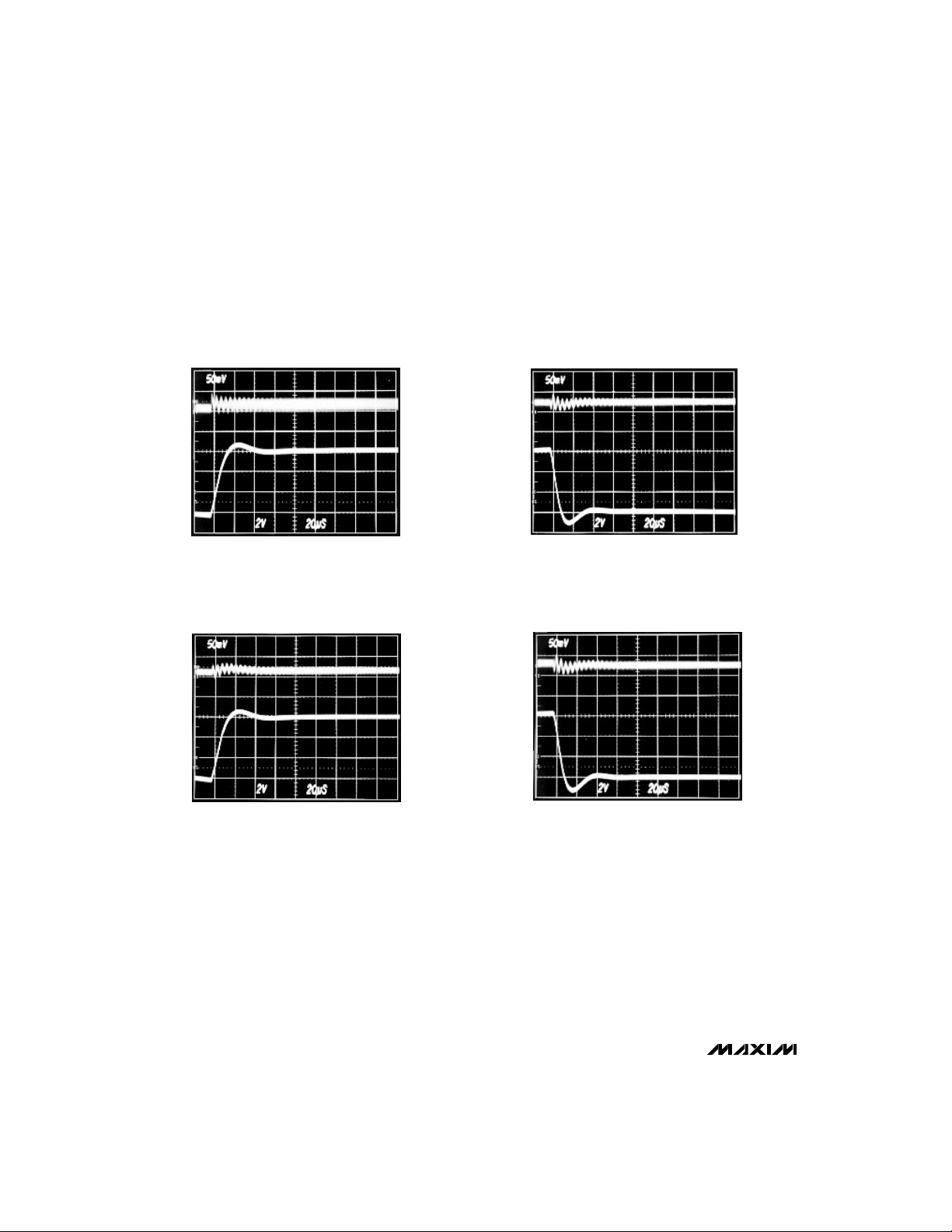
(Circuit of Figure 1, Transpower transformer type TTI5870, VDD ≥ 13V, TA= +25°C, unless otherwise noted.)
+5V LINE-TRANSIENT RESPONSE, RISING
MAX782
HORIZONTAL = 20µs/div
I
= 2A
LOAD
+3.3V LINE-TRANSIENT RESPONSE, RISING
+5V OUTPUT
50mV/div
VIN, 10V TO 16V
2V/div
+3.3V OUTPUT
50mV/div
, 10V TO 16V
V
IN
2V/div
+5V LINE-TRANSIENT RESPONSE, FALLING
HORIZONTAL = 20µs/div
I
= 2A
LOAD
+3.3V LINE-TRANSIENT RESPONSE, FALLING
+5V OUTPUT
50mV/div
VIN, 16V TO 10V
2V/div
+3.3V OUTPUT
50mV/div
, 16V TO 10V
V
IN
2V/div
HORIZONTAL = 20µs/div
I
= 2A
LOAD
HORIZONTAL = 20µs/div
I
= 2A
LOAD
6 _______________________________________________________________________________________
Page 7
Triple-Output Power-Supply
Controller for Notebook Computers
______________________________________________________________Pin Description
PIN
10
NAME FUNCTION
1
2
3
4
5
6
7
8
9
ON3 Logic input to turn on +3.3V. Logic high turns on the regulator. Connect to VL for automatic start-up.
D1
D2
D3
VH
Q3
Q2
Q1
VPPA 0V, 5V, 12V, Hi-Z PCMCIA VPP output. Sources up to 60mA. Controlled by DA0 and DA1.
VDD
VPPB 0V, 5V, 12V, Hi-Z PCMCIA VPP output. Sources up to 60mA. Controlled by DB0 and DB1.11
#1 level-translator/comparator noninverting input. Inverting comparator input is internally connected to
1.650V. Controls Q1. Connect to GND if unused.
#2 level-translator/comparator noninverting input. Inverting comparator input is internally connected to
1.650V. Controls Q2. Connect to GND if unused.
#3 level-translator/comparator noninverting input. Inverting comparator input is internally connected to
1.650V. Controls Q3. Connect to GND if unused.
External supply input for level-translator/comparator. For N-channel FET drive, connect to VDD or external
+13V to +18V supply. For low-battery comparators, connect to +3.3V or +5V (or to VL/REF).
#3 level-translator/comparator output. Sources 20µA from VH when D3 is high. Sinks 500µA to GND
when D3 is low, even with VH = 0V.
#2 level-translator/comparator output. Sources 20µA from VH when D2 is high. Sinks 500µA to GND
when D2 is low, even with VH = 0V.
#1 level-translator/comparator output. Sources 20µA from VH when D1 is high. Sinks 500µA to GND
when D1 is low, even with VH = 0V.
15V flyback input (feedback). A weak shunt regulator conducts 3mA to GND when VDD exceeds 19V.
Also the supply input to the VPP regulators.
MAX782
GND Low-current analog ground12
REF13
SYNC14
DA1, DA0,
DB1, DB0
SS520
21
23 LX5 +5V-supply inductor connection
CS5
DH5 +5V-supply external MOSFET high-side switch-drive output22
3.3V reference output. Sources up to 5mA for external loads. Bypass to GND with 1µF/mA load or
0.22µF minimum.
Oscillator frequency control and synchronization input: Connect to VL or to GND for f = 200kHz; connect
to REF for f = 300kHz. For external synchronization in the 240kHz to 350kHz range, a high-to-low transition causes the start of a new cycle.
Intel 82365 compatible PCMCIA VPP control inputs (see Table 1)15-18
Logic input to turn on +5V. Logic high turns on the regulator. Connect to VL for automatic startup.19 ON5
+5V-supply soft-start control input. Ramp time to full current limit is 1ms/nF of capacitance to GND.
+5V-supply current-sense input. +100mV = current limit in buck mode, -100mV = current limit in flyback
mode (where the ±100mV are referenced to FB5).
_______________________________________________________________________________________ 7
Page 8
Triple-Output Power-Supply
Controller for Notebook Computers
_________________________________________________Pin Description (continued)
PIN NAME FUNCTION
24
25
MAX782
26
27
28
29
30
31
32
33
34
BST5 +5V-supply boost capacitor connection (0.1µF to LX5)
DL5 +5V-supply external MOSFET synchronous-rectifier drive output
PGND Power ground
FB5 +5V-supply feedback input and low-side current-sense terminal
Internal 5V-supply output. Bypass with 4.7µF. This pin is linearly regulated from V+ or switched to the
VL
+5V output to improve efficiency. VL is always on and can source up to 5mA for external loads.
V+ Main (battery) input: 5.5V to 30V
DL3 +3.3V-supply external MOSFET synchronous-rectifier drive output
BST3 +3.3V-supply boost capacitor connection (0.1µF to LX3)
LX3 +3.3V-supply inductor connection
DH3
FB3
CS3 +3.3V-supply current-sense input. Maximum is +100mV referenced to FB3.35
SS3 +3.3V-supply soft-start control input. Ramp time to full current limit is 1ms/nF of capacitance to GND.36
+3.3V-supply external MOSFET high-side switch-drive output
+3.3V-supply feedback and low-side current-sense terminal
Table 1. Truth Table for VPP Control Pins
D_0 D_1 VPP_
0
0
1
1
0
1
0
1
0V
5V
12V
Hi-Z
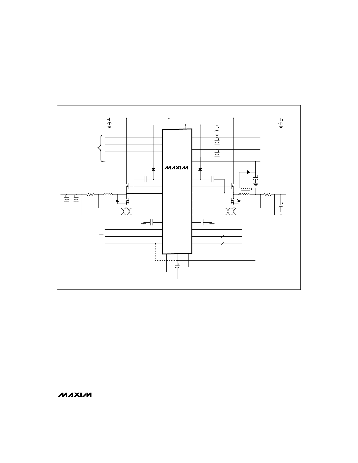
_______________Detailed Description
The MAX782 converts a 5.5V to 30V input to five outputs
(Figure 1). It produces two high-power, switch-mode,
pulse-width modulated (PWM) supplies, one at +5V and
the other at +3.3V. These two supplies operate at either
200kHz or 300kHz, allowing extremely small external
components to be used. Output current capability
depends on external components, and can exceed 5A
on each supply. A 15V high-side (VDD) supply is also
provided, delivering an output current that can exceed
300mA, depending on the external components chosen.
Two linear regulators supplied by the 15V VDD line create programmable VPP supplies for PCMCIA slots.
These supplies (VPPA, VPPB) can be programmed to be
grounded or high impedance, or to deliver 5V or 12V at
up to 60mA.
An internal 5V, 25mA supply (VL) and a 3.3V, 5mA reference voltage (REF) are also generated, as shown in
Figure 2. Fault-protection circuitry shuts off the PWM
and high-side supply when the internal supplies lose
regulation.
Three precision comparators are included. Their output stages permit them to be used as level translators
for driving high-side external power MOSFETs: For
example, to facilitate switching VCC lines to PCMCIA
slots.
8 _______________________________________________________________________________________
Page 9
Triple-Output Power-Supply
Controller for Notebook Computers
MAX782
BATTERY INPUT
5.5V TO 30V
(NOTE 1)
VPP
CONTROL
INPUTS
R1
+3.3V at 3A
C14
150µF
N1-N4 = Si9410DY
NOTE 1: BATTERY VOLTAGE RANGE 6.5V to 30V
WITH COMPONENTS SHOWN
SEE
NOTE 2: SEE FIGURE 5.
25mΩ
C7
150µF
+3.3V ON/OFF
+5V ON/OFF
OSC SYNC
LOW-VOLTAGE (6-CELL) OPERATION
L1
10µH
1N5819
C1
33µF
N1
D3
(NOTE 2)
0.1µF
N3
0.01µF
D1A
1N4148
C5
C9
SECTION.
29 28
V+ VL
16
15
DA1
18
DB0
17
DB1
MAX782
31
BST3
33
DH3
32
LX3
30
DL3
35
CS3
34
FB3
36
SS3
1
ON3
19
ON5
14
SYNC
GND REF PGND
12 13 26
D1-D3
Q1-Q3
C3
1µF
VPPADA0
VPPB
VDD
BST5
DH5
LX5
DL5
CS5
FB5
SS5
C13
+5V at 3A
C6
330µF
33µF
C2
D1B
1N4148
4.7µF
C11
1µF
C4
0.1µF
C8
0.01µF
3
3
C10
1µF
N4
(NOTE 2)
9
11
10
24
22
23
25
21
27
20
5
VH
2, 3, 4
8, 7, 6
+5V at 5mA
0V, 5V, 12V
0V, 5V, 12V
+15V AT 300mA, SEE
HIGH-SIDE SUPPLY (VDD)
D2
EC11FS1
1:2.2
N2
L2 10µH
D4
1N5819
COMPARATOR SUPPLY INPUT
COMPARATOR INPUTS
COMPARATOR OUTPUTS
SECTION.
C12
2.2µF
3.3V AT 5mA
R2
20mΩ
Figure 1. MAX782 Application Circuit
+3.3V Supply
The +3.3V supply is produced by a current-mode PWM
step-down regulator using two small N-channel MOSFETs,
a catch diode, an inductor, and a filter capacitor.
Efficiency is greatly enhanced by the use of the second
MOSFET (connected from LX3 to PGND), which acts as
a synchronous rectifier. A 100nF capacitor connected
to BST3 provides the drive voltage for the high-side
(upper) N-channel MOSFET.
A current limit set by an external sense resistor prevents
excessive inductor current during start-up or under
short-circuit conditions. A soft-start capacitor can be
chosen to tailor the rate at which the output ramps up.
This supply can be turned on by connecting ON3 to
logic high, or can be turned off by connecting ON3 to
GND. All logic levels are TTL and CMOS compatible.
_______________________________________________________________________________________ 9
The +5V output is produced by a current-mode PWM
+5V Supply
step-down regulator similar to the +3.3V supply. This
supply uses a transformer primary as its inductor, the
secondary of which is used for the high-side (VDD)
supply. It also has current limiting and soft-start. It can
be turned off by connecting ON5 to GND, or turned on
by connecting ON5 to logic high.
The +5V supply’s dropout voltage, as configured in
Figure 1, is typically 400mV at 2A. As VINapproaches
5V, the +5V output gracefully falls with VINuntil the VL
regulator output hits its undervoltage lockout threshold.
At this point, the +5V supply turns off.
The default frequency for both PWM controllers is
300kHz (with SYNC connected to REF), but 200kHz
may be used by connecting SYNC to GND or VL.
Page 10
Triple-Output Power-Supply
Controller for Notebook Computers
V+
VL
MAX782
REF
GND
SYNC
VPPA
DA0
DA1
VPPB
DB0
DB1
D3
5V
3.3V
1.65V
+5V LDO
LINEAR
REGULATOR
+3.3V
REFERENCE
300kHz/200kHz
OSCILLATOR
LINEAR
REGULATOR
LINEAR
REGULATOR
2.8V
P
3.3V
PWM
CONTROLLER
(SEE FIG. 3)
ON
5V
PWM
CONTROLLER
(SEE FIG. 3)
ON
4.5V
4V
STANDBY
ON
13V TO 19V
FAULT
VDD REG
13V
FB3
CS3
BST3
DH3
LX3
DL3
SS3
PGND
ON3
FB5
CS5
BST5
DH5
LX5
DL5
SS5
ON5
VDD
19V
Q3
D2
1.65V
D1
1.65V
VH
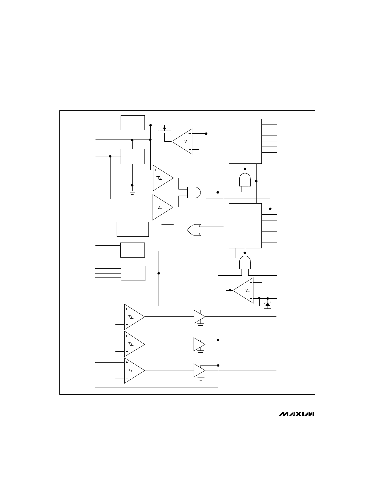
Figure 2. MAX782 Block Diagram
10 ______________________________________________________________________________________
Q2
Q1
Page 11

Triple-Output Power-Supply
Controller for Notebook Computers
CS_
1X
MAX782
REF, 3.3V
(OR INTERNAL
5V REFERENCE)
SS_
ON_
–100mV
60kHz
LPF
MAIN PWM
COMPARATOR
R
Q
S
SLOPE COMP
MINIMUM
CURRENT
N
(IDLE-MODE)
3.3V
VL
30R
1R
SYNCHRONOUS
RECTIFIER CONTROL
0mV-100mV
R
S
CURRENT
LIMIT
Q
25mV
4µA
N
OSC
LEVEL
SHIFT
SHOOT-
THROUGH
CONTROL
LEVEL
SHIFT
FB_
BST_
DH_
LX_
VL
DL_
PGND
N
VDD REG
(SEE FIG. 2)
SINGLE-SHOT
Figure 3. PWM Controller Block Diagram
______________________________________________________________________________________ 11
1µs
Page 12

Triple-Output Power-Supply
Controller for Notebook Computers
+3.3V and +5V PWM Buck Controllers
The two current-mode PWM controllers are identical
except for different preset output voltages and the
addition of a flyback winding control loop to the +5V
side (see Figure 3, +3.3V/+5V PWM Controller Block
Diagram). Each PWM is independent except for being
synchronized to a master oscillator and sharing a common reference (REF) and logic supply (VL). Each PWM
MAX782
can be turned on and off separately via ON3 and ON5.
The PWMs are a direct-summing type, lacking a traditional integrator-type error amplifier and the phase shift
associated with it. They therefore do not require any
external feedback compensation components if the filter capacitor ESR guidelines given in the
Procedure
The main gain block is an open-loop comparator that
sums four input signals: an output voltage error signal,
current-sense signal, slope-compensation ramp, and
precision voltage reference. This direct-summing
method approaches the ideal of cycle-by-cycle control
of the output voltage. Under heavy loads, the controller
operates in full PWM mode. Every pulse from the oscillator sets the output latch and turns on the high-side
switch for a period determined by the duty cycle
(approximately V
off, the synchronous rectifier latch is set and, 60ns later,
the low-side switch turns on (and stays on until the
beginning of the next clock cycle, in continuous mode,
or until the inductor current crosses through zero, in
discontinuous mode). Under fault conditions where the
inductor current exceeds the 100mV current-limit
threshold, the high-side latch is reset and the high-side
switch is turned off.
At light loads, the inductor current fails to exceed the
25mV threshold set by the minimum current comparator. When this occurs, the PWM goes into idle-mode,
skipping most of the oscillator pulses in order to reduce
the switching frequency and cut back switching losses.
The oscillator is effectively gated off at light loads
because the minimum current comparator immediately
resets the high-side latch at the beginning of each
cycle, unless the FB_ signal falls below the reference
voltage level.
A flyback winding controller regulates the +15V VDD
supply in the absence of a load on the main +5V output. If VDD falls below the preset +13V VDD regulation
threshold, a 1µs one-shot is triggered that extends the
on-time of the low-side switch beyond the point where
the inductor current crosses zero (in discontinuous
mode). This causes inductor (primary) current to
reverse, pulling current out of the output filter capacitor
and causing the flyback transformer to operate in the
are followed.
OUT/VIN
). As the high-side switch turns
Design
forward mode. The low impedance presented by the
transformer secondary in forward mode allows the
+15V filter capacitor to be quickly charged again,
bringing VDD into regulation.
Connecting capacitors to SS3 and SS5 allows gradual
build-up of the +3.3V and +5V supplies after ON3 and
ON5 are driven high. When ON3 or ON5 is low, the
appropriate SS capacitors are discharged to GND.
When ON3 or ON5 is driven high, a 4µA constant current source charges these capacitors up to 4V. The
resulting ramp voltage on the SS_ pins linearly increases the current-limit comparator setpoint so as to
increase the duty cycle to the external power MOSFETs
up to the maximum output. With no SS capacitors, the
circuit will reach maximum current limit within 10µs.
Soft-start greatly reduces initial in-rush current peaks
and allows start-up time to be programmed externally.
Synchronous rectification allows for high efficiency by
reducing the losses associated with the Schottky rectifiers. Also, the synchronous rectifier MOSFETS are
necessary for correct operation of the MAX782's boost
gate-drive and VDD supplies.
When the external power MOSFET N1 (or N2) turns off,
energy stored in the inductor causes its terminal voltage to reverse instantly. Current flows in the loop
formed by the inductor, Schottky diode, and load, an
action that charges up the filter capacitor. The Schottky
diode has a forward voltage of about 0.5V which,
although small, represents a significant power loss,
degrading efficiency. A synchronous rectifier, N3 (or
N4), parallels the diode and is turned on by DL3 (or
DL5) shortly after the diode conducts. Since the on
resistance (r
low, the losses are reduced.
The synchronous rectifier MOSFET is turned off when
the inductor current falls to zero.
Cross conduction (or “shoot-through”) is said to occur
if the high-side switch turns on at the same time as the
synchronous rectifier. The MAX782’s internal breakbefore-make timing ensures that shoot-through does not
occur. The Schottky rectifier conducts during the time
that neither MOSFET is on, which improves efficiency
by preventing the synchronous-rectifier MOSFET’s
lossy body diode from conducting.
The synchronous rectifier works under all operating conditions, including discontinuous-conduction and idle-mode.
The +5V synchronous rectifier also controls the 15V VDD
voltage (see the
) of the synchronous rectifier is very
DS(ON)
High-Side Supply (VDD)
Soft-Start/SS_ Inputs
Synchronous Rectifiers
section).
12 ______________________________________________________________________________________
Page 13

Triple-Output Power-Supply
Controller for Notebook Computers
Gate-drive voltage for the high-side N-channel switch is
Boost Gate-Driver Supply
generated with a flying-capacitor boost circuit as shown
in Figure 4. The capacitor is alternately charged from
the VL supply via the diode and placed in parallel with
the high-side MOSFET’s gate-source terminals. On startup, the synchronous rectifier (low-side) MOSFET forces
LX_ to 0V and charges the BST_ capacitor to 5V. On the
second half-cycle, the PWM turns on the high-side
MOSFET by connecting the capacitor to the MOSFET
gate by closing an internal switch between BST_ and
DH_. This provides the necessary enhancement voltage
to turn on the high-side switch, an action that “boosts”
the 5V gate-drive signal above the battery voltage.
Ringing seen at the high-side MOSFET gates (DH3 and
DH5) in discontinuous-conduction mode (light loads) is
a natural operating condition caused by the residual
energy in the tank circuit formed by the inductor and
stray capacitance at the LX_ nodes. The gate driver
negative rail is referred to LX_, so any ringing there is
directly coupled to the gate-drive supply.
Modes of Operation
PWM Mode
Under heavy loads – over approximately 25% of full load
– the +3.3V and +5V supplies operate as continuous-current PWM supplies (see
Characteristics
). The duty cycle (%ON) is approximately:
%ON = V
Typical Operating
OUT/VIN
Current flows continuously in the inductor: First, it
ramps up when the power MOSFET conducts; then, it
ramps down during the flyback portion of each cycle
as energy is put into the inductor and then discharged into the load. Note that the current flowing
into the inductor when it is being charged is also
flowing into the load, so the load is continuously
receiving current from the inductor. This minimizes
output ripple and maximizes inductor use, allowing
very small physical and electrical sizes. Output ripple is primarily a function of the filter capacitor (C7 or
C6) effective series resistance (ESR) and is typically
under 50mV (see the
Design Procedure
section).
Output ripple is worst at light load and maximum
input voltage.
Idle Mode
Under light loads (<25% of full load), efficiency is further enhanced by turning the drive voltage on and off
for only a single clock period, skipping most of the
clock pulses entirely. Asynchronous switching, seen as
“ghosting” on an oscilloscope, is thus a normal operating
BATTERY
INPUT
VL
VL
LEVEL
TRANSLATOR
PWM
Figure 4. Boost Supply for Gate Drivers
BST_
DH_
LX_
VL
DL_
condition whenever the load current is less than
approximately 25% of full load.
At certain input voltage and load conditions, a transition
region exists where the controller can pass back and
forth from idle-mode to PWM mode. In this situation,
short bursts of pulses occur that make the current
waveform look erratic, but do not materially affect the
output ripple. Efficiency remains high.
Current Limiting
The voltage between CS3 (CS5) and FB3 (FB5) is continuously monitored. An external, low-value shunt resistor is
connected between these pins, in series with the inductor, allowing the inductor current to be continuously measured throughout the switching cycle. Whenever this
voltage exceeds 100mV, the drive voltage to the external
high-side MOSFET is cut off. This protects the MOSFET,
the load, and the battery in case of short circuits or temporary load surges. The current-limiting resistor R1 (R2)
is typically 25mΩ (20mΩ) for 3A load current.
Oscillator Frequency; SYNC Input
The SYNC input controls the oscillator frequency.
Connecting SYNC to GND or to VL selects 200kHz operation; connecting to REF selects 300kHz operation. SYNC
can also be driven with an external 240kHz to 350kHz
CMOS/TTL source to synchronize the internal oscillator.
Normally, 300kHz is used to minimize the inductor and
filter capacitor sizes, but 200kHz may be necessary for
low input voltages (see
Low-Voltage (6-cell) Operation
MAX782
).
______________________________________________________________________________________ 13
Page 14

Triple-Output Power-Supply
Controller for Notebook Computers
The 15V VDD supply is obtained from the rectified and
filtered secondary of transformer L2. VDD is enabled
whenever the +5V supply is on (ON5 = high). The primary and secondary of L2 are connected so that, during the flyback portion of each cycle (when MOSFET
N2 is off and N4 is on), energy stored in the core is
transferred into the +5V load through the primary and
MAX782
into VDD through the secondary, as determined by the
turns ratio. The secondary voltage is added to the +5V
to make VDD. See the
Characteristics
Unlike other coupled-inductor flyback converters, the
VDD voltage is regulated regardless of the loading on
the +5V output. (Most coupled-inductor converters can
only support the auxiliary output when the main output
is loaded.) When the +5V supply is lightly loaded, the
circuit achieves good control of VDD by pulsing the
MOSFET normally used as the synchronous rectifier.
This draws energy from the +5V supply’s output capacitor and uses the transformer in a forward-converter
mode (i.e., the +15V output takes energy out of the
secondary when current is flowing in the primary).
Note that these forward-converter pulses are interspersed with normal synchronous-rectifier pulses, and
they only occur at light loads on the +5V rail.
The transformer secondary’s rectified and filtered output is only roughly regulated, and may be between 13V
and 19V. It is brought back into VDD, which is also the
feedback input, and used as the source for the PCMCIA
VPP regulators (see
for the VDD supply’s load capability.
Generating Additional VPP Outputs
Using External Linear Regulators
as the VH power supply for the comparators or any
external MOSFET drivers.
When the input voltage is above 20V, or when the +5V
supply is heavily loaded and VDD is lightly loaded, L2’s
interwinding capacitance and leakage inductance can
produce voltages above that calculated from the turns
ratio. A 3mA shunt regulator limits VDD to 19V.
Clock-frequency noise on the VDD rail of up to 3Vp-p is
a facet of normal operation, and can be reduced by
adding more output capacitance.
Typical Operating
). It can also be used
PCMCIA-Compatible
Programmable VPP Supplies
Two independent regulators are provided to furnish
PCMCIA VPP supplies. The VPPA and VPPB outputs
can be programmed to deliver 0V, 5V, 12V, or to be high
impedance. The 0V output mode has a 250Ω pull-down
to discharge external filter capacitors and ensure that
flash EPROMs cannot be accidentally programmed.
These linear regulators operate from the high-side sup-
High-Side Supply (VDD)
Table 2. VPP Program Codes
DA0 DA1 VPPA
0
0
1
1
DB0 DB1 VPPB
0
0
1
1
ply (VDD), and each can furnish up to 60mA. Bypass
VPPA and VPPB to GND with at least 1µF, with the
bypass capacitors less than 20mm from the VPP pins.
The outputs are programmed with DA0, DA1, DB0 and
DB1, as shown in Table 2.
These codes are Intel 82365 (PCMCIA digital controller)
compatible. For other interfaces, one of the inputs can
be permanently wired high or low and the other toggled
to turn the supply on and off. The truth table shows that
either a “0” or “1” can be used to turn each supply on.
The high-impedance state is to accomodate external
programming voltages. The two VPP outputs can be
safely connected in parallel for increased load capability
if the control inputs are also tied together (i.e., DA0 to
DB0, DA1 to DB1). If VPAA and VPPB are connected in
parallel, some devices may exhibit several milliamps of
increased quiescent supply current when enabled, due
to slightly mismatched output voltage set points.
Three noninverting comparators can be used as precision voltage comparators or high-side drivers. The
supply for these comparators (VH) is brought out and
may be connected to any voltage between +3V and
+19V. The noninverting inputs (D1-D3) are high impedance, and the inverting input is internally connected to
a 1.650V reference. Each output (Q1-Q3) sources
20µA from VH when its input is above 1.650V, and
sinks 500µA to GND when its input is below 1.650V.
The Q1-Q3 outputs can be fixed together in wired-OR
configuration since the pull-up current is only 20µA.
Connecting VH to a logic supply (5V or 3V) allows the
comparators to be used as low-battery detectors. For driving N-channel power MOSFETs to turn external loads on
and off, VH should be 6V to 12V higher than the load voltage. This enables the MOSFETs to be fully turned on and
results in low r
DS(ON)
0
1
0
1
0
1
0
1
. VDD is a convenient source for VH.
0V
5V
12V
Hi-Z
0V
5V
12V
Hi-Z
Comparators
14 ______________________________________________________________________________________
Page 15

Triple-Output Power-Supply
Controller for Notebook Computers
The comparators are always active when V+ is above
+4V, even when VH is 0V. Thus, Q1-Q3 will sink current
to GND even when VH is 0V, but they will only source
current from VH when VH is above approximately 1.5V.
If Q1, Q2, or Q3 is externally pulled above VH, an internal diode conducts, pulling VH a diode drop below the
output and powering anything connected to VH. This
voltage will also power the other comparator outputs.
Internal VL and REF Supplies
An internal linear regulator produces the 5V used by the
internal control circuits. This regulator’s output is available on pin VL and can source 5mA for external loads.
Bypass VL to GND with 4.7µF. To save power, when
the +5V switch-mode supply is above 4.5V, the internal
linear regulator is turned off and the high-efficiency +5V
switch-mode supply output is connected to VL.
The internal 3.3V bandgap reference (REF) is powered
by the internal 5V VL supply, and is always on. It can
furnish up to 5mA. Bypass REF to GND with 0.22µF,
plus 1µF/mA of load current.
Both the VL and REF outputs remain active, even when
the switching regulators are turned off, to supply memory keep-alive power.
These linear-regulator ouputs can be directly connected
to the corresponding step-down regulator outputs (i.e.,
REF to +3.3V, VL to +5V) to keep the main supplies alive
in standby mode. However, to ensure start-up, standby
load currents must not exceed 5mA on each supply.
Fault Protection
The +3.3V and +5V PWM supplies, the high-side supply, and the comparators are disabled when either of
two faults is present: VL < +4.0V or REF < +2.8V (85%
of its nominal value).
__________________Design Procedure
Figure 1’s schematic and Table 2’s component list
show values suitable for a 3A, +5V supply and a 3A,
+3.3V supply. This circuit operates with input voltages
from 6.5V to 30V, and maintains high efficiency with
output currents between 5mA and 3A (see the
Operating Characteristics
). This circuit’s components
may be changed if the design guidelines described in
this section are used – but before beginning the design,
the following information should be firmly established:
V
, the maximum input (battery) voltage. This
IN(MAX)
value should include the worst-case conditions under
which the power supply is expected to function, such
Typical
as no-load (standby) operation when a battery charger
is connected but no battery is installed. V
not exceed 30V.
V
, the minimum input (battery) voltage. This
IN(MIN)
value should be taken at the full-load operating current under the lowest battery conditions. If V
is below about 6.5V, the power available from the
IN(MAX)
can-
IN(MIN)
VDD supply will be reduced. In addition, the filter
capacitance required to maintain good AC load regulation increases, and the current limit for the +5V
supply has to be increased for the same load level.
+3.3V Inductor (L1)
Three inductor parameters are required: the inductance
value (L), the peak inductor current (I
coil resistance (RL). The inductance is:
V
where: V
x (V
OUT
L = ————————————-
V
IN(MAX)
= output voltage, 3.3V;
OUT
V
f = switching frequency, normally 300kHz;
I
LIR = ratio of inductor peak-to-peak AC
= maximum input voltage (V);
IN(MAX)
= maximum +3.3V DC load current (A);
OUT
IN(MAX)
x f x I
OUT
- V
OUT
x LIR
)
LPEAK
), and the
current to average DC load current, typically 0.3.
A higher value of LIR allows smaller inductance, but
results in higher losses and higher ripple.
The highest peak inductor current (I
DC load current (I
inductor current (I
current is typically chosen as 30% of the maximum DC
) plus half the peak-to-peak AC
OUT
). The peak-to-peak AC inductor
LPP
LPEAK
) equals the
load current, so the peak inductor current is 1.15 times
I
.
OUT
The peak inductor current at full load is given by:
I
LPEAK
x (V
= I
OUT
OUT
+ —————————————.
2 x f x L x V
IN(MAX)
- V
IN(MAX)
OUT
)
V
The coil resistance should be as low as possible,
preferably in the low milliohms. The coil is effectively in
series with the load at all times, so the wire losses alone
are approximately:
Power loss = I
OUT
2
x R
L
In general, select a standard inductor that meets the L,
I
, and RLrequirements (see Tables 3 and 4). If a
LPEAK
standard inductor is unavailable, choose a core with an
LI2parameter greater than L x I
largest wire that will fit the core.
LPEAK
2
, and use the
MAX782
______________________________________________________________________________________ 15
Page 16

Triple-Output Power-Supply
Controller for Notebook Computers
Table 3 lists two commercially available transformers
+5V Transformer (T1)
and parts for a custom transformer. The following
instructions show how to determine the transformer
parameters required for a custom design:
LP, the primary inductance value
I
, the peak primary current
LPEAK
LI2, the core’s energy rating
MAX782
RPand RS, the primary and secondary resistances
N, the primary-to-secondary turns ratio.
The transformer primary is specified just as the +3.3V
inductor, using V
(VDD)
power
= +5.0V; but the secondary output
OUT
must be added in as if it were part of the
primary. VDD current (IDD) usually includes the VPPA
and VPPB output currents. The total +5V power, P
is the sum of these powers:
P
= P5 + P
where: P5 = V
TOTAL
PDD= VDD x IDD;
and: V
OUT
I
OUT
VDD = VDD output voltage, 15V;
OUT
= output voltage, 5V;
= maximum +5V load current (A);
x I
OUT
DD
;
IDD= maximum VDD load current (A);
so: P
and the equivalent +5V output current, I
TOTAL
I
TOTAL
= (5V x I
= P
TOTAL
= [(5V x I
) + (15V x IDD)
OUT
/ 5V
) + (15V x IDD)] / 5V.
OUT
TOTAL
, is:
The primary inductance, LP, is given by:
V
where: V
x (V
OUT
LP= ———————————————
V
= output voltage, 5V;
OUT
V
IN(MAX)
f = switching frequency, normally 300kHz;
I
= maximum equivalent load current (A);
TOTAL
LIR = ratio of primary peak-to-peak AC
x f x I
IN(MAX)
= maximum input voltage;
IN(MAX)
TOTAL
- V
OUT
x LIR
)
current to average DC load current, typically 0.3.
The highest peak primary current (I
total DC load current (I
AC primary current (I
current is typically chosen as 30% of the maximum DC
) plus half the peak-to-peak
TOTAL
). The peak-to-peak AC primary
LPP
LPEAK
) equals the
load current, so the peak primary current is 1.15 times
I
. A higher value of LIR allows smaller inductance,
TOTAL
but results in higher losses and higher ripple.
The peak current in the primary at full load is given by:
V
x (V
I
= I
LPEAK
Choose a core with an LI2parameter greater than LPx
I
LPEAK
TOTAL
2
.
OUT
+ —————————————.
2 x f x LPx V
IN(MAX
) - V
OUT
IN(MAX)
)
TOTAL
The winding resistances, RPand RS, should be as low
as possible, preferably in the low milliohms. Use the
largest gauge wire that will fit on the core. The coil is
effectively in series with the load at all times, so the
resistive losses in the primary winding alone are
approximately (I
The minimum turns ratio, N
to accommodate the tolerance of the +5V supply. A
TOTAL
)2x RP.
, is 5V:(15V-5V). Use 1:2.2
MIN
greater ratio will reduce efficiency of the VPP regulators.
Minimize the diode capacitance and the interwinding
capacitance, since they create losses through the
VDD shunt regulator. These are most significant when
the input voltage is high, the +5V load is heavy, and
there is no load on VDD.
,
Ensure the transformer secondary is connected with the
right polarity: A VDD supply will be generated with either
polarity, but proper operation is possible only with the correct polarity. Test for correct connection by measuring the
VDD voltage when VDD is unloaded and the input voltage
(VIN) is varied over its full range. Correct connection is
indicated if VDD is maintained between 13V and 20V.
Current-Sense Resistors (R1, R2)
The sense resistors must carry the peak current in the
inductor, which exceeds the full DC load current.
The internal current limiting starts when the voltage
across the sense resistors exceeds 100mV nominally,
80mV minimum. Use the minimum value to ensure
adequate output current capability: For the +3.3V
supply, R1 = 80mV / (1.15 x I
R2 = 80mV/(1.15 x I
TOTAL
); for the +5V supply,
OUT
), assuming that LIR = 0.3.
Since the sense resistance values (e.g. R1 = 25mΩ for
I
= 3A) are similar to a few centimeters of narrow
OUT
traces on a printed circuit board, trace resistance can
contribute significant errors. To prevent this, Kelvin
connect the CS_ and FB_ pins to the sense resistors;
i.e., use separate traces not carrying any of the inductor or load current, as shown in Figure 5.
Run these traces parallel at minimum spacing from one
another. The wiring layout for these traces is critical for
stable, low-ripple outputs (see the
Grounding
section).
Layout and
MOSFET Switches (N1-N4)
The four N-channel power MOSFETs are usually identical and must be “logic-level” FETs; that is, they must
be fully on (have low r
source drive voltage. The MOSFET r
ideally be about twice the value of the sense resistor.
MOSFETs with even lower r
capacitance, which increases switching time and
) with only 4V gate-
DS(ON)
have higher gate
DS(ON)
DS(ON)
transition losses.
should
16 ______________________________________________________________________________________
Page 17

Triple-Output Power-Supply
Controller for Notebook Computers
FAT, HIGH-CURRENT TRACES
MAIN CURRENT PATH
KELVIN SENSE TRACES
MAX782
Figure 5. Kelvin Connections for the Current-Sense Resistors
SENSE RESISTOR
MOSFETs with low gate-threshold voltage specifications (i.e., maximum V
preferred, especially for high-current (5A) applications.
= 2V rather than 3V) are
GS(TH)
Output Filter Capacitors (C6, C7, C14)
The output filter capacitors determine the loop stability
and output ripple voltage. To ensure stability, the minimum capacitance and maximum ESR values are:
V
CF> —————————————
V
OUT
REF
x RCSx 2 x π x GBWP
and,
V
x R
OUT
ESRCF< ——————
CS
V
REF
where: CF= output filter capacitance, C6 or C7 (F);
= reference voltage, 3.3V;
V
REF
= output voltage, 3.3V or 5V;
V
OUT
= sense resistor (Ω);
R
CS
GBWP = gain-bandwidth product, 60kHz;
= output filter capacitor ESR (Ω).
ESR
CF
Be sure to select output capacitors that satisfy both the
minimum capacitance and maximum ESR requirements. To achieve the low ESR required, it may be
appropriate to use a capacitance value 2 or 3 times
larger than the calculated minimum.
The output ripple in continuous-current mode is:
V
OUT(RPL)
= I
LPP(MAX)
x (ESRCF+1/(2 x π x f x CF)).
In idle-mode, the ripple has a capacitive and resistive
component:
4 x 10⁻⁴x L
V
(C) = ——————— x
OUT(RPL)
2
R
x C
CS
F
1 1
——— + ————— ) Volts
(
V
OUTVIN
V
OUT(RPL)
The total ripple, V
lows:
if V
OUT(RPL)
then V
OUT(RPL)
otherwise, V
OUT(RPL)
V
OUT(RPL)
- V
OUT
0.02 x ESR
(R) = ——————- Volts
, can be approximated as fol-
OUT(RPL)
(R) < 0.5 V
= V
OUT(RPL)
= 0.5 V
(R).
R
CS
OUT(RPL)
(C),
OUT(RPL)
CF
(C),
(C) +
Diode D2
The voltage rating of D2 should be at least 2 x VIN+
5V plus a safety margin. A rating of at least 75V is
necessary for the maximum 30V supply. A Schottky
diode is preferable for lower input voltages, and is
required for input voltages under 7V. Use a highspeed silicon diode (with a higher breakdown voltage
and lower capacitance) for high input voltages. D2’s
current rating should exceed twice the maximum current load on VDD.
Diodes D3 and D4
Use 1N5819s or similar Schottky diodes. D3 and D4
conduct only about 3% of the time, so the 1N5819’s
1A current rating is conservative. The voltage rating
of D3 and D4 must exceed the maximum input supply
voltage from the battery. These diodes must be
Schottky diodes to prevent the lossy MOSFET body
diodes from turning on, and they must be placed
physically close to their associated synchronous rectifier MOSFETs.
Soft-Start Capacitors (C8, C9)
A capacitor connected from GND to either SS pin causes that supply to ramp up slowly. The ramp time to full
current limit, tSS, is approximately 1ms for every nF of
capacitance on SS_, with a minimum value of 10µs.
Typical capacitor values are in the 10nF to 100nF
range; a 5V rating is sufficient.
MAX782
______________________________________________________________________________________ 17
Page 18

Triple-Output Power-Supply
Controller for Notebook Computers
Because this ramp is applied to the current-limit circuit,
the actual time for the output voltage to ramp up
depends on the load current and output capacitor
value. Using Figure 1’s circuit with a 2A load and no
SS capacitor, full output voltage is reached about
600µs after ON_ is driven high.
MAX782
Capacitors C4 and C5 store the boost voltage and pro-
Boost Capacitors (C4, C5)
vide the supply for the DH3 and DH5 drivers. Use 0.1µF
and place each within 10mm of the BST_ and LX_ pins.
Boost Diodes (D1A, D1B)
Use high-speed signal diodes; e.g., 1N4148 or equivalent.
Table 3. Surface-Mount Components
(See Figure 1 for schematic diagram and Table 4 for phone numbers.)
33µF, 35V tantalum capacitors
1N4148SMTN diodes (fast recovery)
Transformer (these two have different
sizes and pinouts)
Transformer (for 5.5V, 200kHz operation)
Custom Transformer:
L2
Core Set
Bobbin
Clamp
Primary
Secondary
Bypass Capacitors
Input Filter Capacitors (C1, C13)
Use at least 3µF/W of output power for the input filter
capacitors, C1 and C13. They should have less than
150mΩ ESR, and should be located no further than
10mm from N1 and N2 to prevent ringing. Connect
the negative terminals directly to PGND. Do not
exceed the surge current ratings of input bypass
capacitors.
VPP and VDD Bypass Capacitors (C10, C11, C12)
Use 2.2µF for VDD, and 1µF for VPPA and VPPB.
PART NO.MANUFACTURERSPECIFICATIONCOMPONENT
595D336X0035R2BSpragueC1, C13
Sprague
Sprague
Murata-Erie
Sprague
Sprague
NihonFast-recovery high voltage diodeD2
Coiltronics
Transpower Technologies
TDK
TDK
TDK
595D475X0016A2B4.7µF, 16V tantalum capacitorC2
595D475X0016A2B1µF, 20V tantalum capacitorC3
GRM42-6X7R104K50V0.1µF, 16V ceramic capacitorsC4, C5
595D337X0010R2BSprague330µF, 10V tantalum capacitorC6
595D157X0010D2BSprague150µF, 10V tantalum capacitorsC7, C14
GRM42-6X7R103K50VMurata-Erie0.01µF, 16V ceramic capacitorsC8, C9
595DD105X0035A2B1µF, 35V tantalum capacitorsC10, C11
595DD225X0025B2B2.2µF, 25V tantalum capacitorC12
BAW56PhilipsD1A, D1B
EC11FS1
EC10QS04Nihon1N5819 SMT diodesD3, D4
CDR125-100Sumida10µH, 2.65A inductorL1
Si9410DYSiliconixN-channel MOSFETs (SO-8)N1-N4
LR2010-01-R025-FIRC0.025Ω, 1% (SMT) resistorR1
LR2010-01-R020-FIRC0.020Ω, 1% (SMT) resistorR2
CTX03-12067-1
TTI5870
CTX03-12062-1Coiltronics
PC40EEM12.7/13.7-A160
BEM12.7/13.7-118G
FEM12.7/13.7-A
8 turns #24 AWG
18 turns #26 AWG
18 ______________________________________________________________________________________
Page 19

Triple-Output Power-Supply
Controller for Notebook Computers
Table 4. Surface-Mount Components
Company USA Phone
Central Semi
Coiltronics
IRC
Murata-Erie
Nihon
Siliconix
Sprague
Sumida
TDK
Transpower Tech.
Factory FAX
[country code]
[ 1] (516) 435-1824
[ 1] (407) 241-9339
[ 1] (213) 772-9028
[ 1] 404 736-3030
[81] 3-3494-7414
[ 1] (408) 727-5414
[ 1] (603) 224-1430
[81] 3-3607-5144
[81] 3-3278-5358
[ 1] 702 831-3521
(516) 435-1110
(407) 241-7876
(512) 992-7900
(404) 736-1300
(805) 867-2555
(408) 988-8000
(603) 224-1961
(708) 956-0666
(708) 803-6100
(702) 831-0140
__________Applications Information
Achieving outstanding efficiency over a wide range of
loads is a result of balanced design rather than bruteforce overkill, particularly with regard to selecting the
power MOSFETs. Generally, the best approach is to
design for two loading conditions, light load and heavy
load (corresponding to suspend and run modes in the
host computer), at some nominal battery voltage (such
as 1.2V/cell for NiCd or NiMH). Efficiency improves as
the input voltage is reduced, as long as the high-side
switch saturation voltage is low relative to the input voltage. If there is a choice, use the lowest-voltage battery
pack possible, but with at least six cells.
Losses due to parasitic resistances in the switches,
coil, and sense resistor dominate at high load-current
levels. Under heavy loads, the MAX782 operates in the
continuous-conduction mode, where there is a large
DC offset to the inductor current plus a small sawtooth
AC component (see the
DC current is exactly equal to the load current – a fact
that makes it easy to estimate resistive losses through
the assumption that total inductor current is equal to
this DC offset current.
Efficiency Considerations
Heavy-Load Efficiency
+3.3V Inductor
section). This
The major loss mechanisms under heavy loads are, in
usual order of importance:
2
● I
R losses
● gate-charge losses
● diode-conduction losses
● transition losses
● capacitor-ESR losses
● losses due to the operating supply current of the IC.
Inductor core losses are fairly low at heavy loads
because the inductor current’s AC component is small.
Therefore, they are not accounted for in this analysis.
Efficiency = P
PD
TOTAL
PD
= resistive loss = (I
(I2R)
where R
COIL
the drain-source on resistance of the MOSFET, and
OUT/PIN
PD
= PD
(I2R)
PD
CAP
is the DC resistance of the coil, r
TOTAL
+ PD
+ PD
x 100% = P
) x 100%
+ PD
GATE
IC
2
) x (R
LOAD
RCS)
DIODE
COIL
OUT
+ PD
/(P
+ r
OUT
TRAN
DS(ON)
DS(ON)
RCSis the current-sense resistor value. Note that the
r
employed for both the synchronous rectifier and high-
term assumes that identical MOSFETs are
DS(ON)
side switch, because they time-share the inductor current. If the MOSFETs are not identical, losses can be
estimated by averaging the two individual r
terms according to duty factor.
PD
= gate driver loss = qGx f x VL
GATE
DS(ON)
where VL is the MAX782’s logic supply voltage (nominally 5V) and qGis sum of the gate charge for lowside and high-side switches. Note that gate charge
losses are dissipated in the IC, not the MOSFETs,
and therefore contribute to package temperature rise.
For matched MOSFETs, qGis simply twice the gate
charge of a single MOSFET (a data sheet specification). If the +5V buck SMPS is turned off, replace VL
in this equation with VIN.
P
= diode conduction losses = I
DIODE
LOAD
x VDx tDx f
where tDis the diode’s conduction time (typically
110ns), VDis the forward voltage of the Schottky diode,
and f is the switching frequency.
2
V
x C
x I
PD
= transition loss = ———————————
TRAN
IN
RSS
I
DRIVE
LOAD
x f
MAX782
+
+
+
is
______________________________________________________________________________________ 19
Page 20

Triple-Output Power-Supply
Controller for Notebook Computers
where C
high-side MOSFET (a data sheet parameter), f is the
switching frequency, and I
available from the MAX782’s large high-side gate dri-
is the reverse transfer capacitance of the
RSS
is the peak current
DRIVE
ver outputs (DH5 or DH3, approximately 1A).
Additional switching losses are introduced by other
sources of stray capacitance at the switching node,
including the catch diode capacitance, coil interwind-
MAX782
ing capacitance, and low-side switch-drain capacitance. They are given as PDSW= V
but are usually negligible compared to C
The low-side switch introduces only tiny switching
2
x C
IN
STRAY
RSS
losses, since its drain-source voltage is already low
when it turns on.
PD
= capacitor ESR loss = I
CAP
RMS
2
x ESR
and,
I
= RMS AC input current
RMS
= I
√ V
x ————————
LOAD
OUT(VIN
V
IN
- V
OUT
)
where ESR is the equivalent series resistance of the
input bypass capacitor. Note that losses in the output
filter capacitors are small when the circuit is heavily
loaded, because the current into the capacitor is not
chopped. The output capacitor sees only the small AC
sawtooth ripple current. Ensure that the input bypass
capacitor has a ripple current rating that exceeds the
value of I
RMS
.
PDICis the IC’s quiescent power dissipation and is a data
sheet parameter (6mW typically for the entire IC at VIN=
15V). This power dissipation is almost completely independent of supply voltage whenever the +5V step-down
switch-mode power supply is on, since power to the chip
is bootstrapped from the +5V output. When calculating
the efficiency of each individual buck controller, use 3mW
for PDIC, since each controller consumes approximately
half of the total quiescent supply current.
Example: +5V buck SMPS at 300kHz, VIN= 15V, I
= 2A, RCS= R
Si9410DY with r
= 30nC.
PD
(DIODE) + 22mW (TRAN) + 22mW (CAP) + 3mW (IC)
= 400mW (I2R) + 90mW (GATE) + 36mW
TOTAL
= ESR = 25mΩ, both transistors are
COIL
DS(ON)
= 0.05Ω, C
= 160pF, and q
RSS
= 573mW
Efficiency = 10W/(10W + 573mW) x 100% = 94.6%
(actual measured value = 94%).
Light-Load Efficiency
Under light loads, the PWMs operate in the discontinuous-conduction mode, where the inductor current discharges to zero at some point during each switching
x f,
losses.
LOAD
cycle. New loss mechanisms, insignificant at heavy
loads, start to become important. The basic difference
is that, in discontinuous mode, the inductor current’s
AC component is large compared to the load current.
This increases core losses and losses in the output filter capacitors. Ferrite cores are recommended over
powdered toroid types for best light-load efficiency.
At light loads, the inductor delivers triangular current
pulses rather than the nearly constant current found in
continuous mode. These pulses ramp up to a point set
by the idle-mode current comparator, which is internally
fixed at approximately 25% of the full-scale current-limit
level. This 25% threshold provides an optimum balance between low-current efficiency and output voltage
noise (the efficiency curve would actually look better if
this threshold were set at about 45%, but the output
noise would then be too high).
Reducing I
specifying huge, low-r
atrocious efficiency, especially at mid-range and light-
2
R losses though the brute-force method of
MOSFETs can result in
DS(ON)
load conditions. Even at heavy loads, the gate charge
losses introduced by huge 50A MOSFETs usually more
than offset any gain obtained through lower r
Layout and Grounding
Good layout is necessary to achieve the designed output power, high efficiency, and low noise. Good layout
includes use of a ground plane, appropriate component placement, and correct routing of traces using
appropriate trace widths. The following points are in
order of importance:
1. A ground plane is essential for optimum performance.
In most applications, the power supply is located on a
multilayer motherboard, and full use of the four or
more copper layers is recommended. Use the top
and bottom layers for interconnections, and the inner
layers for an uninterrupted ground plane.
2. Keep the Kelvin-connected current-sense traces
short, close together, and away from switching
nodes. See Figure 5.
G
3. Place the LX node components N1, N3, D3, and L1
as close together as possible. This reduces resistive
and switching losses and keeps noise due to
ground inductance confined. Do the same with the
other LX node components N2, N4, D4, and L2.
4. The input filter capacitor C1 should be less than
10mm away from N1’s drain. The connecting copper trace carries large currents and must be at least
2mm wide, preferably 5mm.
Similarly, place C13 close to N2’s drain, and connect them with a wide trace.
DS(ON)
.
20 ______________________________________________________________________________________
Page 21

Triple-Output Power-Supply
Controller for Notebook Computers
5. Keep the gate connections to the MOSFETs short for
low inductance (less than 20mm long and more than
0.5mm wide) to ensure clean switching.
6. To achieve good shielding, it is best to keep all
high-voltage switching signals (MOSFET gate drives DH3 and DH5, BST3 and BST5, and the two LX
nodes) on one side of the board and all sensitive
nodes (CS3, CS5, FB3, FB5 and REF) on the other
side.
7. Connect the GND and PGND pins directly to the
ground plane, which should ideally be an inner layer
of a multilayer board.
8. Connect the bypass capacitor C2 very close (less
than 10mm) to the VL pin.
9. Minimize the capacitance at the transformer secondary. Place D5 and C12 very close to each other
and to the secondary, then route the output to the IC’s
VDD pin with a short trace. Bypass with 0.1µF close
to the VDD pin if this trace is longer than 50mm.
The layout for the evaluation board is shown in the
Evaluation Kit
section. It provides an effective, low-
noise, high-efficiency example.
Power-Ready and Power Sequencing
A “power-ready” signal can be generated from one of
the comparator outputs by connecting one of the supplies (e.g., the +5V output – see Figure 6) through a
high-resistance voltage divider to the comparator input.
The threshold for the +5V-output comparator is set by
R1 and R2 according to the formula: VTH= 1.65V x (R1
+ R2) / R2. For example, choosing R1 = 1MΩ and R2 =
604kΩ sets the nominal threshold to 4.38V.
If the power-ready signal is required to indicate when
both the +3.3V and the +5V supplies have come up,
use the MAX707 supervisory circuit shown in Figure 7.
The threshold for the +3.3V-line comparator is set by
R1 and R2 according to the formula: VTH= 1.25V x (R1
+ R2) / R2. For example, choosing R1 = 1.2MΩ and R2
= 1MΩ sets the nominal threshold to 2.75V. The threshold for the +5V supply is preset inside the MAX707,
and is typically 4.65V. The reset outputs remain asserted while either supply line is below its threshold, and
for at least 140ms after both lines are fully up.
If sequencing of the +3.3V and +5V supplies is critical,
several approaches are possible. For example, the
SS3 and SS5 capacitors can be sized to ensure that
the two supplies come up in the desired order. This
technique requires that the SS capacitors be selected
specifically for each individual situation, because the
loading on each supply affects its power-up speed.
+5V
SUPPLY
FB5
1M
R1
D_
604k
R2
Figure 6. Power-Ready Signal for the +5V Supply
+5V
SUPPLY
+3.3V
SUPPLY
R1
1.24M
R2
1M
Figure 7. Power-Ready Signal Covers Both +3.3V and +5V
Supplies with External Voltage Monitor IC (MAX707)
V
CC
4.65V
PFI
1.25V
GND
1.65V
MAX782
GND
RESET
MAX707
Q_
RESET
RESET
MR
PFO
+5V
POWER-READY
POWER READY
POWER READY
Another approach uses the “power-ready” comparator
output signal (see Figure 6) from one supply as a control input to the ON_ pin of the other supply.
MAX782
______________________________________________________________________________________ 21
Page 22

Triple-Output Power-Supply
Controller for Notebook Computers
+5V SUPPLY
VCC
GND
C4
100nF
P
HYST1
OUT2
N
POWER READY
R6
R3
C1
22nF
1M
1M
+3.3V SUPPLY
R4
1M
MAX782
SET1
C2
100
nF
R5
820k
R1
1M
SET2
R2
390k
ICL7665
1.3V
Figure 8. Power-Up Sequencing for the Intel 486SL
Figure 8 shows a more complex example of power
sequencing. On power-up, the Intel 486SL computer
requires the +5V supply to come up before the +3.3V
supply. A power-ready signal is required ≥50ms later.
This circuit’s ON3 output connects to the MAX782’s
ON3 pin, and can be wire-OR connected with an opendrain output to enable another circuit to turn the +3.3V
supply off.
PCMCIA Slot +3.3V/+5V VCC Switching
The MAX782 contains level shifters that simplify driving
external power MOSFETs to switch PCMCIA card VCC
to 3.3V and 5V. While a PCMCIA card is being inserted
into the socket, the VCC pins on the card edge should
be powered down to 0V so “hot insertion” does not
damage the PCMCIA card. The simplest way to do this
is to use a mechanical switch that has to be physically
opened before the PCMCIA card can be inserted. The
switch, which disconnects VCC, can be closed only
when the card has been fitted snugly into its socket.
Figure 9’s circuit illustrates this approach and correctly
shows the connections to both MOSFETs: N2 appears
to be inserted with drain and source the wrong way
around, but this is necessary to prevent its body diode
from pulling the +3.3V supply up to 5V when VCC is
connected to the +5V supply.
ON3
C3
100nF
g
+3.3V SUPPLY
s
N2
d
+5V SUPPLY
d
N1
s
SLOT
VCC
MECHANICAL
SWITCH
VDD VH
FB5
PCMCIA 2.0
DIGITAL
CONTROLLER
VCC_EN0
VCC_EN1
NOTE: MOSFET BODY DIODES SHOWN FOR CLARITY.
D1
D2
MAX782
FB3
Q1
Q2
g
Figure 9. Simple Switching for PCMCIA Slot VCC
FB5
PCMCIA 2.0
DIGITAL
CONTROLLER
VCC_EN0
VCC_EN1
NOTE: MOSFET BODY DIODES SHOWN FOR CLARITY.
D1
D2
MAX782
VDD
FB3
VH
+5V
Q1
+3.3V
Q2
N3
SLOT
VCC
N1
N2
100µF
Figure 10. Using the Level Shifters to Switch PCMCIA Slot VCC
Figure 10’s circuit provides an alternative method of
connecting the VCC supply to the PCMCIA slot. While
it avoids using a mechanical switch, it does not provide
the security of a physical interlock. Placing the two
MOSFETs N1 and N2 with their body diodes facing in
opposite directions allows VCC to be shut down to 0V
without using a mechanical switch, and allows VCC to
be driven to 5V without the +3.3V supply being pulled
up to 5V.
22 ______________________________________________________________________________________
Page 23

Triple-Output Power-Supply
Controller for Notebook Computers
Table 5. Components for Low-Voltage
Operation
(Circuit of Figure 1, f = 200kHz, VINRange = 5.5V to 12V)
Coiltronics CTX03-12062
Transformer L2:
Filter Capacitor C6: 660µF
Sense Resistor: 25mΩ
Flyback Rectifier D2:
The MAX782 has three comparators/level-shifters that
can be used for this purpose, and two that are needed for
each PCMCIA port. Two transistors can be used as
shown in Figure 11 to provide two additional TTL-input
MOSFET gate drivers for a second PCMCIA slot. The
component values have been carefully chosen to provide
smooth switching from 5V to 3.3V without make-beforebreak glitches, and without a break in the VCC supply.
Low-Voltage (6-Cell) Operation
Low input voltages, such as the 6V end-of-life voltage of
a 6-cell NiCd battery, place extra demands on the +5V
buck regulator because of the very low input-output differential voltage. The standard application circuit works
well with supply voltages down to 6.5V; at input voltages
less than 6.5V, some component changes are needed
(see Table 5), and the operating frequency must be set
to 200kHz. The two main issues are load-transient
response and load capability of the +15V VDD supply.
The +5V supply’s load-transient response is impaired due
to reduced inductor-current slew rate, which is in turn
caused by reduced voltage applied across the buck inductor during the high-side switch-on time. So, the +5V output
sags when hit with an abrupt load current change, unless
the +5V filter capacitor value is increased. Note that only the
capacitance is affected and ESR requirements don’t
change. Therefore, the added capacitance can be supplied by an additional low-cost bulk capacitor in parallel with
the normal low-ESR switching-regulator capacitor. The
equation for voltage sag under a step-load change follows:
V
= —————————————————
SAG
2 x CFx (V
where DMAX is the maximum duty cycle. Higher duty
cycles are possible when the oscillator frequency is
reduced to 200kHz, due to fixed propagation delays
through the PWM comparator becoming a lesser part of
the whole period. The tested worst-case limit for DMAX
is 92% at 200kHz. Lower inductance values can reduce
(low-leakage inductance,
10µH primary)
1N5819 or equivalent
Schottky diode
2
I
x L
STEP
x DMAX - V
IN(MIN)
OUT
)
MAX782
VDD FB5 FB3
1M
+5V
+3.3V
PCMCIA 2.0
DIGITAL
CONTROLLER
VCC_EN0
VCC_EN1
NOTE: MOSFET BODY DIODES SHOWN FOR CLARITY.
Figure 11. Using Discrete Circuitry to Switch PCMCIA 2.0 Slot VCC
1M
1M
510k
2N3904
2N3904
SLOT
VCC
100µF
the filter capacitance requirement, but only at the
expense of increased noise at high input voltages (due
to higher peak currents).
The components shown in Table 5 allow the main +5V
supply to deliver 2A from V
allow the +15V supply to deliver 70mA while simultane-
= 5.5V, or alternatively
IN
ously providing +5V at 2A from VIN= 5.7V. Note:
Components for +3.3V don’t need to be changed.
The +15V supply’s load capability is also affected by
low input voltages, especially under heavy loads. When
the +5V supply is heavily loaded, there simply isn’t
enough extra duty cycle left for the flyback winding
controller to deliver energy to the secondary. VDD loadcurrent limitations are thus determined by the worstcase duty-cycle limits, and also by any parasitic resistance or inductance on the transformer secondary.
These parasitics, most notably the transformer leakage
inductance and the forward impedance of the +15V
rectifier diode, limit the rate-of-rise of current in the secondary during the brief interval when primary current
reverses and the transformer conducts in the forward
mode. See the
Typical Operating Characteristics
. For
low-voltage applications that require heavy +15V load
currents (for example, 6-cell circuits where +12V VPP
must deliver 120mA or more), see the MAX783 data
sheet. This device is similar to the MAX782 except the
+15V flyback winding controller has been shifted from
the +5V side to the +3.3V side.
MAX782
______________________________________________________________________________________ 23
Page 24

Triple-Output Power-Supply
Controller for Notebook Computers
When the +5V and +3.3V supplies are off, the complete
Total Shutdown Circuits
MAX782 circuit consumes only about 70µA, plus any
leakage through the off MOSFETs. Some NiCd batteries can be damaged if they are fully discharged and
then left for long periods (months) under load. Even
100µA can do damage if left long enough.
The complete power-supply system can be shut down
MAX782
by taking ON5 low, cutting the supply to the MAX782’s
V+ pin, while the bootstrapped +5V supply is turned
off. This removes the supply from the controller, and
turns off all the supplies. In this condition, the current
consumption drops to the level of the leakage currents
in the off transistors. Switching the V+ supply off is
easy because the V+ line draws very little power;
switching the entire power input from the battery would
be more difficult.
Figure 12 shows a logic interface for a momentary
switch that toggles the whole system on and off. The
logic circuit runs from the battery supply, so the input
voltage from the battery is limited to the normal operating range for the flip-flop gates, which is usually 18V for
4000-series CMOS circuits. The active-high OFF input
permits the supplies to be turned off under logic control
as well as when the switch is pushed. If this logic input
is not required, omit R1 and Q1. The supplies can only
be turned on using the hardware switch. For automatic
turn-off, connect the OFF input to a battery-voltage
sensing comparator or to a timer powered from VL.
Ensure that any signal connected to OFF does not
glitch high at power-up.
Generating Additional VPP Outputs
Using External Linear Regulators
Figure 13 shows a low-dropout linear regulator
designed to provide an additional VPP output from the
VDD line. It can be turned off with a logic-level signal;
its output can be switched to 5V or 12V; and it provides excellent rejection of the high-frequency noise
on VDD. If a monolithic linear regulator is used,
choose one having good PSRR performance at
300kHz.
(+5.5V TO +18V)
V
BATT
OFF
1µF
CD4011B
1N4148
1M
1M
1N4148
1M
R1
1M
S
R
Q1
2N4401
1N4148
1N4148
ON
ON
1M
VL
MAX782
ON5
PGND
ON5
ON/
OFF
1M
1µF
Figure 12. Hardware/Software Total Shutdown Circuit
VDD
FROM MAX782
100nF
FROM MAX782
REF
R5
100k
OFF/ON
C1
3
OP27
2
C4
10nF
Q2
2N7002
Q1
2N4403
R4
C3
1k
10nF
7
U1
6
4
12/5
R1
16.9k
Q3
2N7002
6.8µF
R2
6.34k
R3
26.7k
ZETEX
ZVP2106G
SOT 223
V+
C2
OUT
OFF/ON
1
00 5
01 12
X = DON'T CARE
12/5 V
X0
Figure 13. External Regulator For Additional VPP Outputs
24 ______________________________________________________________________________________
(V)
OUT
Page 25

Triple-Output Power-Supply
Controller for Notebook Computers
________Evaluation Kit Information
The MAX782 evaluation kit (EV kit) is an assembled,
surface-mount demonstration board. The kit embodies
the standard application circuit and uses dip switches
to control the 3V, 5V, and VPP outputs. The board
accepts battery input voltages between 6.5V and 30V,
and provides up to 30W of output power. All functions
are controlled by standard CMOS/TTL logic levels.
___________Ev Kit Quick Reference
To set up the EV kit, use the following procedure:
1. Connect a power supply to the BATT IN terminals.
The supply voltage should be between 6.5V and 30V.
Input current may be several amps, depending on the
input voltage and the output power demanded.
2. Turn on the +5V output by setting the ON5 dip
switch to ON. The 5V OUT edge pad now supplies
+5V at up to 3A, and +15V is now available at the
+15V OUT edge pad.
3. Turn on the +3.3V output by setting the ON3 dip
switch to ON. The 3.3V OUT edge pad now supplies +3.3V at up to 3A. The two regulators may be
operated independently.
4. To use the VPPA/VPPB programmable voltage outputs, ON5 must be enabled. Set the four-circuit dip
switch to the desired code and measure the output at
the VPPA and VPPB edge pads. DA0 and DA1 control VPPA’s state; DB0 and DB1 control VPPB’s state.
_______Ev Kit Detailed Description
Battery Input
BATT IN – Battery input, 6.5V to 30V
GND – Ground
The battery input voltage should be between 6.5V and
30V. The input voltage upper limit is set by the voltage
rating of the input bypass capacitors, C1 and C13, and
may not exceed the MAX782’s 30V maximum rating.
Higher input voltages generally require physically larger input capacitors.
Low-Battery Detection Comparators
To demonstrate the level shifters / high-side drivers,
ON5 must be enabled so the +15V (VDD) is available
to pull up the Q1-Q3 outputs. Measure the high-side
driver supply at the VH edge pad. Logic-level edge
pads D1-D3 control the outputs Q1-Q3. Q1-Q3 pull up
to VH whenever the corresponding input D1-D3 is at a
logic-high level.
When active, outputs Q1-Q3 pull up to VH. Resistor
R16, located on the back of the board, pulls the highside driver voltage VH up to +15V. By removing R16
and installing a resistor at the empty R15 site, VH may
be tied to the +3.3V output. Alternately, both R15 and
R16 may be omitted and the user may supply an arbitrary voltage between 3V and 20V at the VH edge pad.
Note that Q1-Q3 are not meant to drive high-current
loads directly.
The D1-D3 comparators can be used as precision voltage detectors by installing resistor dividers at each
input (R11/R12, R10/R13, R9/R14).
Power-Supply Controls
ON3 – Enable 3.3V power supply
ON5 – Enable 5.0V power supply
SYNC – Switch-mode power-supply frequency input
(optional)
VPP Voltage Outputs
The PCMCIA-compatible programmable voltage outputs are controlled by the DA0, DA1, DB0, and DB1
logic-level inputs. The MAX782 provides industrystandard Intel 82365-comptaible VPPA/VPPB PCMCIA
controls (see
switch connects the same way as the edge pads.
From left to right, switch 1 controls DA1, switch 2 controls DA0, switch 3 controls DB1, and switch 4 controls
DB0. VPPA and VPPB are capable of supplying 60mA
each.
Pin Description
). The four-circuit dip
MAX782
______________________________________________________________________________________ 25
Page 26

Triple-Output Power-Supply
Controller for Notebook Computers
5V
C6
D2
25V
2.2µF
L2
EC11FS1
N2
22
DH5
OUT
C6
330µF
10V
R2
0.02Ω
D4
1N5819
N4
23
25
21
27
LX5
DL5
DL335CS3
30
CS5
FB513REF
FB3
34
MAX782
BATT IN
VPPB
VH
35V
C13
33µF
C1
35V
33µF
R15
OPEN
5VH28VL9
29
V+
VPPA
R16
560Ω
C2
4.7µF
16V
11
VPPA
VPPB
+15V
OUT
35V
C11
1µF
35V
C10
1µF
C4
0.1µF
D1
10
24
VDD
BST5
MAX782
DA116DA017DB118DB0
15
BST333DH332LX3
31
D1
SYNC
N1–N4 = Si9410DY
D1 = BAW56L OR TWO 1N4148s
C3
1µF
20V
R17
100k
14
SYNC
ON3
ON5
1
19
Q1
8
Q1
2D13
Q2
7Q26
D2
Q3
C8
0.01µF
Q3
12 26 20
SS3 GND PGND SS5
36
D3
C9
4
0.01µF
C5
0.1µF
R6
1M
R5
1M
R4
1M
R3
1M
DA1
DA0
DB1
DB0
X2A
X2B
X2C
X2D
N1
R1
N3
D3
L1
1N5819
10µH
0.025Ω
X1A
X1B
R12 OPEN
10V
C16
150µF
C7
10V
150µF
3.3V
OUT
ON3
ON5
D18
Figure 14. MAX782 EV Kit Schematic
26 ______________________________________________________________________________________
R13 OPEN
D2B
R14 OPEN
D3B
1M
R11
1M
R10
R9
1M
R7
1M
R8
1M
Page 27

Triple-Output Power-Supply
Controller for Notebook Computers
MAX782
Figure 15. MAX782 EV Kit Top Component Layout and Silk Screen, Top View
______________________________________________________________________________________ 27
Page 28

Triple-Output Power-Supply
Controller for Notebook Computers
MAX782
Figure 16. MAX782 EV Kit Ground Plane (Layers 2 and 3), Top View
28 ______________________________________________________________________________________
Page 29

Triple-Output Power-Supply
Controller for Notebook Computers
MAX782
Figure 17. MAX782 EV Kit Top Layer (Layer 1), Top View
______________________________________________________________________________________ 29
Page 30

Triple-Output Power-Supply
Controller for Notebook Computers
MAX782
Figure 18. MAX782 EV Kit, Bottom Component Layout and Silk Screen, Bottom View
30 ______________________________________________________________________________________
Page 31

Triple-Output Power-Supply
Controller for Notebook Computers
MAX782
Figure 19. MAX782 EV Kit Bottom Layer (Layer 4), Top View
______________________________________________________________________________________ 31
Page 32

Triple-Output Power-Supply
Controller for Notebook Computers
___________________Chip Topography _Ordering Information (continued)
D2
ON3
D3
VH
Q3
Q2
Q1
MAX782
VPPA
VDD
VPPB
GND
CS3
DH3
SS3
FB3
LX3
BST3
DL3
V+
VL
FB5
PGND
DL5
0.181"
(4.597mm)
* Contact factory for dice specifications.
D1
PIN-PACKAGETEMP. RANGEPART
Dice*0°C to +70°CMAX782C/D
36 SSOP-40°C to +85°CMAX782EBX
36 SSOP-40°C to +85°CMAX782REBX
BOARD TYPETEMP. RANGEEV KIT
Surface Mount0°C to +70°CMAX782EVKIT-SO
V
OUT
—
3.3V
3.45V
3.6V36 SSOP-40°C to +85°CMAX782SEBX
SYNC
REF
DA1
DA0
DB1
ON5
DB0
0.132"
(3.353mm)
SS5
CS5
DH5
BST5
LX5
TRANSISTOR COUNT: 1569
SUBSTRATE CONNECTED TO GND
________________________________________________________Package Information
INCHES MILLIMETERS
DIM
A
A1
B
C
HE
D
D
E
e
H
L
α
α
A
0.127mm
A1
e
B
0.004in.
C
L
MAX
MIN
0.094
0.004
0.011
0.009
0.604
0.292
0.398
0.020
0˚
0.104
0.011
0.017
0.012
0.610
0.298
0.416
0.035
8˚
MIN
2.39
0.10
0.30
0.23
15.34
7.42
10.10
0.51
0˚
0.80 BSC0.032 BSC
36-PIN PLASTIC
SHRINK
SMALL-OUTLINE
PACKAGE
MAX
2.64
0.28
0.44
0.32
15.49
7.57
10.57
0.89
8˚
21-0032A
Maxim cannot assume responsibility for use of any circuitry other than circuitry entirely embodied in a Maxim product. No circuit patent licenses are
implied. Maxim reserves the right to change the circuitry and specifications without notice at any time.
32
__________________Maxim Integrated Products, 120 San Gabriel Drive, Sunnyvale, CA 94086 (408) 737-7600
© 1994 Maxim Integrated Products Printed USA is a registered trademark of Maxim Integrated Products.
 Loading...