

Page 1
19-0205; Rev 0; 7/94
EVALUATION KIT
AVAILABLE
PDA/Hand-Held Computer Power Controller
_______________General Description
The MAX781 is a system-engineered power-supply controller for subnotebook computers, PDAs, or similar battery-powered equipment. It provides high-performance,
step-down (buck), pulse-width modulated (PWM) control
for generating +3.3V and constant-current battery charging. Dual PCMCIA VPP outputs are powered by a regulated flyback winding. Five high-side gate drivers and a
buffered analog multiplexer are also included. All functions are controlled by an SPI/Microwire™ compatible
four-wire serial interface.
The MAX781 generates +3.3V with high efficiency through
synchronous rectification and PWM operation at heavy
loads. It uses Idle Mode™ operation at light loads. Only
small external components are required because of the
device’s high switching frequency (300kHz) and advanced
current-mode PWM architecture that allows for output
capacitance as low as 50µF per ampere of load.
The MAX781 is configured by 32 bits of serial data. These
bits select the operating mode, set the switch-mode battery charger current level, select one of eight analog multiplexer channels, and turn on/off the five high-side gate
drivers. A status byte read from the serial interface indicates if the battery has been removed, if the DC charging
source has been connected, or if there is a fault condition
on the +3.3V output. An interrupt output signals the CPU if
a status signal changes.
____________________________Features
♦ +3.3V Step-Down Controller
♦ Dual PCMCIA 2.0 Compatible VPP Outputs
(0V/3.3V/5V/12V)
♦ Digitally Adjustable Switching Current Source for
Battery Charging
♦ 5 High-Side Switch Gate-Driver Outputs
♦ SPI Serial Interface
♦ 300kHz Switching Frequency
♦ Oscillator SYNC Input
♦ 2.5V ±1.5% Reference Output
♦ 36-Pin SSOP Package
________________________Applications
Subnotebook Computers
PDAs
Communicating Computers
Handy-Terminals
______________Ordering Information
PART
MAX781CBX
MAX781EBX -40°C to +85°C
TEMP. RANGE PIN-PACKAGE
0°C to +70°C
36 SSOP
36 SSOP
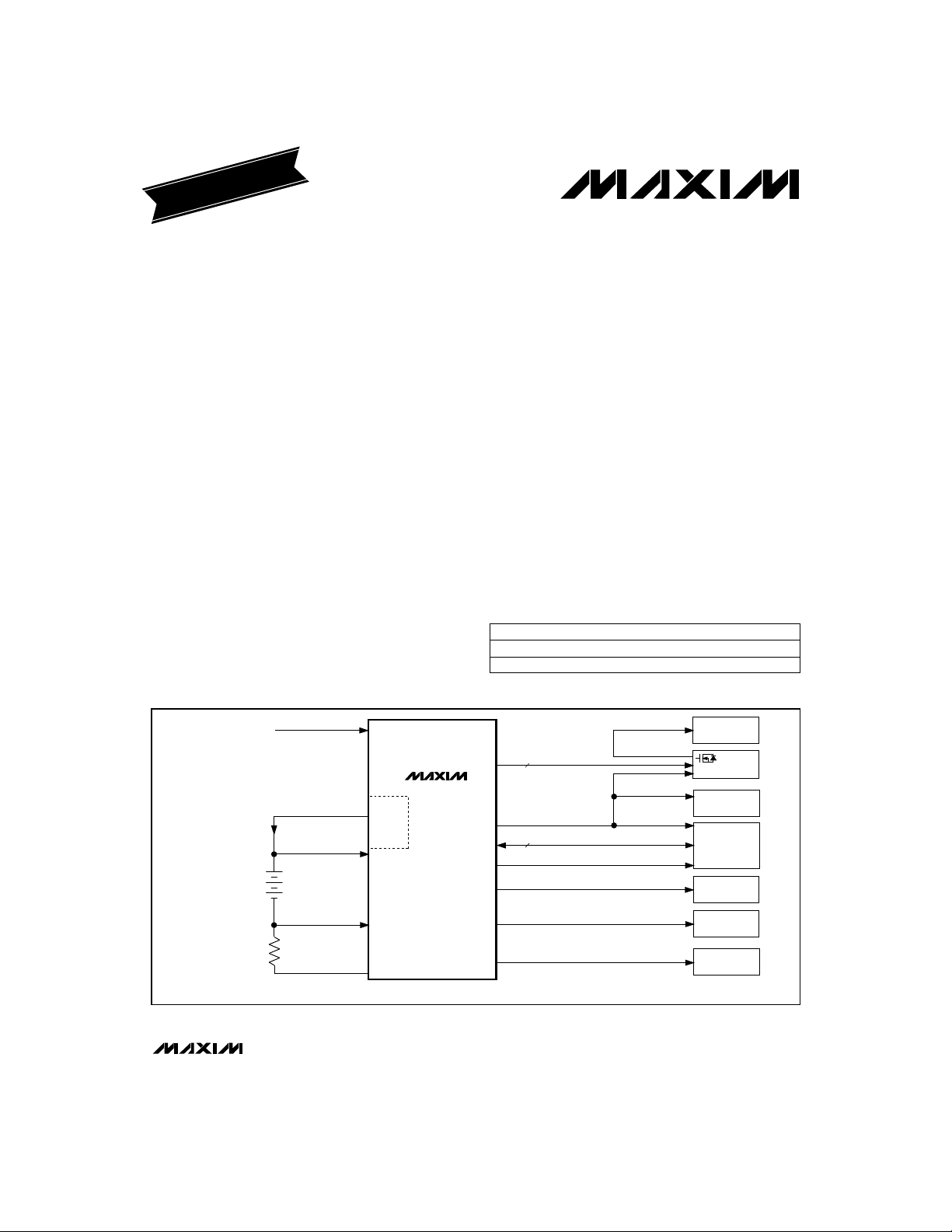
________________________________________________Typical Application Diagram
(up to 18V)
5 to 8
NiCd/NiMH
CELLS
or
2 LION
CELLS
DCIN
DIGITALLY
ADJUSTABLE
SWITCHING
CURRENT
SOURCE
MAX781
HIGH-SIDE GATE DRIVERS
5
+3.3V AT 1A OR MORE
SERIAL INTERFACE
4
INTERRUPT
VPPA
VPPB
ANALOG MULTIPLEXER OUTPUT
SUBSYSTEMS
LOAD
SWITCHES
SELF REFRESH
DRAM
CPU
PCMCIA
SLOT A
PCMCIA
SLOT B
ADC
MAX781
Pin Configuration on last page.
™
SPI is a trademark of Motorola Inc. Microwire is a trademark of National Semiconductor Corp.
Idle Mode is a trademark of Maxim Integrated Porducts.
________________________________________________________________
Maxim Integrated Products
Call toll free 1-800-998-8800 for free samples or literature.
1
Page 2
PDA/Hand-Held Computer Power Controller
ABSOLUTE MAXIMUM RATINGS
BATT, VCHG, VHI to AGND.........................................-0.3V, 20V
VPPA, VPPB to AGND..................................................-0.3V, 20V
FAST, GD1, GD2, GD3, GD4, GD5 to AGND..............-0.3V, 20V
BST to AGND...............................................................-0.3V, 30V
BST to LX.......................................................................-0.3V, 7V
DHI to LX.......................................................-0.3V, (BST + 0.3V)
PGND to AGND........................................................-0.3V, +0.3V
MAX781
All Other Pins to AGND or PGND ..................................-0.3V, 7V
VPPA, VPPB Current.........................................................100mA
Stresses beyond those listed under “Absolute Maximum Ratings” may cause permanent damage to the device. These are stress ratings only, and functional
operation of the device at these or any other conditions beyond those indicated in the operational sections of the specifications is not implied. Exposure to
absolute maximum rating conditions for extended periods may affect device reliability.
ELECTRICAL CHARACTERISTICS
(BATT = 6V, power-on reset state, TA= T
MIN
to T
, unless otherwise noted.)
MAX
5OUT Current....................................................................100mA
3OUT Current......................................................................40mA
Continuous Power Dissipation (T
SSOP (derate 11.76mW/°C above +70°C) ....................941mW
Operating Temperature Ranges
MAX781CBX .........................................................0°C to +70°C
MAX781EBX......................................................-40°C to +85°C
Storage Temperature Range.............................-65°C to +150°C
Lead Temperature (soldering, 10sec).............................+300°C
= +70°C)
A
SUPPLY AND REFERENCE
BATT Quiescent Supply Current
5OUT Output Voltage
Internal Undervoltage Lockout
Threshold (measured at 5OUT,
UVLO = AGND)
UVLO Threshold
(measured at UVLO)
INTERNAL OSCILLATOR
Internal Oscillator Frequency
CONDITIONS
Shutdown mode, –S—H—D—N–= 0V
Low-power mode, –S—H—D—N–= BATT = 18V
Standby mode, –S—H—D—N–= BATT = 18V
Operate mode, –S—H—D—N–= BATT = 18V
No load
I
= -20µA to 100µA
SOURCE
Operate or standby mode, 5.5V < BATT < 18V,
0mA < I
Low-power mode, 5.5V < BATT < 18V,
0mA < I
V
5OUT
V
5OUT
V
UVLO
V
UVLO
SYNC = REF
SYNC = AGND or 5OUT
5OUT
5OUT
rising
falling
rising
falling
< 25mA
< 10mA
10
60 120
250 750
4.8 5.2
4.8 5.2
4.30 4.60 4.80
4.10 4.35 4.50
97 103
90 96
270 300 340
170 230 260
UNITSMIN TYP MAXPARAMETER
µA
mA12
V2.463 2.5 2.537REF Output Voltage
mV-20 20REF Load Regulation
V
V
%REF
nA50UVLO Input Bias Current
kHz
kHz270 350SYNC Capture Range (Note 1)
ns500SYNC Minimum Pulse Width (Note1)
ns200SYNC Fall Time (Note 1)
µs1SYNC Rise Time (Note 1)
V0.75SYNC Input Voltage Low
V3.8SYNC Input Voltage High
nA-100 100SYNC Leakage Current
2 _______________________________________________________________________________________
Page 3
PDA/Hand-Held Computer Power Controller
ELECTRICAL CHARACTERISTICS (continued)
(BATT = 6V, power-on reset state, TA= T
3.3V OUTPUT
DLO On-Resistance
BATTINT Battery-Detect
Threshold (measured at TEMP)
VPP REGULATOR
VPP_Output Voltage
HIGH-SIDE GATE DRIVERS
to T
MIN
Low-power mode, 4V < BATT < 18V, 0mA < I
Standby mode, 4V < BATT < 18V, 0mA < I
Operate mode, 4V < BATT < 18V,
CS to 3OUT = 0mV to 80mV
3OUT falling
High, 5OUT = 4.75V
Low, 5OUT = 4.75V
High or low, BST - LX = 4.5V
TEMP falling
TEMP rising
Operate mode V12.8 13.5 14.2VHI Regulation Threshold
Operate mode,
I
SINK
VPPA1 = VPPA0 = 0,
VPPB1 = VPPB0 = 0,
GDSEL1 to GDSEL5 = 0
VHI = 20V
Operate mode,
VHI = 18V,
VPPA1 = VPPA0 = 0,
VPPB1 = VPPB0 = 0,
GDSEL1 to GDSEL5 = 0
I
SINK
VPP_1 = 0, VPP_0 = 0
14.2V < VHI < 18V, VPP_1 = 0, VPP_0 = 1,
0mA < IVPP_ < 60mA
14.2V < VHI < 18V, VPP_1 = 1, VPP_0 = 0,
0mA < IVPP_ < 60mA
14.2V < VHI < 18V, VPP_1 = 1, VPP_0 = 1,
0mA < IVPP_ < 60mA
VHI = 14.2V, GDSEL_ = 1,
I
SOURCE
VHI = 14.2V, GDSEL_ = 0,
I
SINK
GD_ = 2.5V, GDSEL_ = 1,
VHI = 14.2V
GD_ = 2.5V, GDSEL_ = 0,
VHI = 14.2V
, unless otherwise noted.)
MAX
= 200µA,
= 1mA,
= 1µA
= 20µA
CONDITIONS
3OUT
3OUT
< 1mA
< 10mA
3.17 3.43
3.17 3.43
3.17 3.43
15
10
75 81
83 89
0.25
4.75 5.0 5.25
11.4 12.0 12.6
3.14 3.3 3.49
MAX781
UNITSMIN TYP MAXPARAMETER
V3OUT Output Voltage
mV80 100 130CS to 3OUT Current-Limit Threshold
V2.9 3.0 3.13VINT Fault-Detect Threshold
mV1503VINT Fault-Detect Hysteresis
Ω
Ω10DHI On-Resistance
%3OUT
V20VHI Clamp Voltage
mA1VHI Clamp Current
µA45VHI Input Bias Current
V
V14GD_ Output High Voltage
V0.25GD_ Output Low Voltage
µA61018GD_ Source Current
µA200 450 900GD_ Sink Current
_______________________________________________________________________________________ 3
Page 4
PDA/Hand-Held Computer Power Controller
ELECTRICAL CHARACTERISTICS (continued)
(BATT = 6V, power-on reset state, TA= T
ANALOG MULTIPLEXER
MAX781
AOUT Output Voltage
SERIAL INTERFACE
CE, SCLK, DIN Logic Input High
Voltage
CE, SCLK, DIN Logic Input Low
Voltage
DOUT, INT Logic Output High
Voltage
DOUT, INT Logic Output Low
Voltage
CE, SCLK, DIN Logic Input
Rise/Fall Time (Note 1)
BATTERY CHARGER
CSBAT Full-Scale Current-Sense
Voltage
COMP Current-Sense Amplifier
Offset Voltage
Current-Sense Amplifier CSBAT to
COMP Transconductance (gm)
FAST OUTPUT
Output Sink Current
to T
MIN
MUX2 = 0, MUX1 = 0, MUX0 = 0
MUX2 = 0, MUX1 = 0, MUX0 = 1
MUX2 = 0, MUX1 = 1, MUX0 = 0
MUX2 = 0, MUX1 = 1, MUX0 = 1
MUX2 = 1, MUX1 = 0, MUX0 = 0
MUX2 = 1, MUX1 = 0, MUX0 = 1
MUX2 = 1, MUX1 = 1, MUX0 = 0
MUX2 = 1, MUX1 = 1, MUX0 = 1
I
SINK
I
SOURCE
I
SINK
High or low, 5OUT = 4.75V
CHG6 to CHG0 = 1,
CHARGE = 1
CSBAT = 0V mV-2 0 2
FAST = 3V, FASTON = 1
FAST = 18V, FASTON = 0
, unless otherwise noted.)
MAX
= 10µA
= 1mA
= 1.6mA
CONDITIONS
UNITSMIN TYP MAXPARAMETER
%3OUT65.33 66.67 68.00
%5OUT44.54 45.45 46.36
%BATT19.90 20.00 20.10
%TEMP65.33 66.67 68.00
%VPPA18.49 18.87 19.25
%VPPB18.49 18.87 19.25
%VREF99.8 100 100.2
%AUXIN65.33 66.67 68.00
mV10AOUT Output Low
V2
V0.8
nA-100 100SCLK, DIN Leakage Current
kΩ60 100 140CE Internal Pull-Down Resistance
V2.7
V0.4
ns50
Ω10DCHG On Resistance
mV190 200 210
µmho400 600 750
mA1.0 2.0
nA±1.0
4 _______________________________________________________________________________________
Page 5
PDA/Hand-Held Computer Power Controller
TIMING CHARACTERISTICS (Note 1)
PARAMETER MIN TYP MAX UNITS
DIN to SCLK Data Setup Time 125 ns
DIN to SCLK Data Hold Time
SCLK to DOUT Valid Propagation Delay 30 200 ns
SCLK Clock Period 400 ns
SCLK High Pulse Width 125 ns
SCLK Low Pulse Width 125 ns
CE Assertion to DOUT Enable 120 ns
CE Deassertion to DOUT Disable 120 ns
CE Assertion to SCLK Rising-Edge
Setup Time
SCLK Rising Edge to CE Deassertion 200 ns
CE High Pulse Width 300 ns
SCLK Rising Edge to CE Assertion 200 ns
CE Deassertion to SCLK Rising Edge 200 nst
Note 1: Guaranteed by design.
SYMBOL
t
DS
t
DH
t
DO
t
CP
t
CH
t
CL
t
DV
t
TR
t
CSS
t
CSH
t
CSW
t
CS0
CS1
0 ns
200 ns
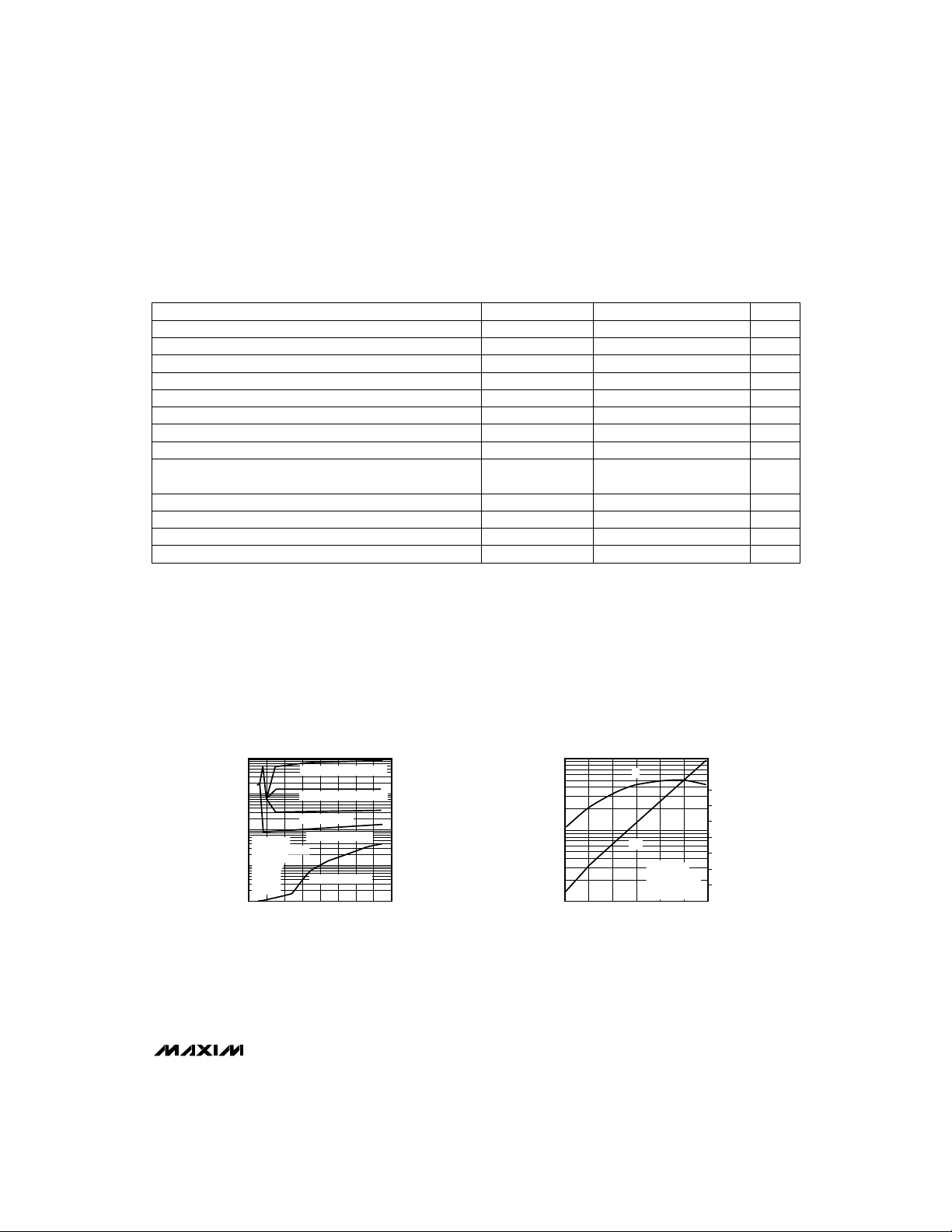
__________________________________________Typical Operating Characteristics
(TA = +25°C, unless otherwise noted.)
MAX781
NO LOAD SUPPLY CURRENT
10
1
0.1
(I
=0mA)
3OUT
SYNC=UVLO=AGND,
CHARGE=0
GDSEL_=0
0.01
QUIESCENT CURRENT (mA)
MUX_=0
5ON=1
VPP_=0
0.001
2 4 6 8 10 12 14 16 18
OPERATE MODE (IDLE = 0)
OPERATE MODE (IDLE = 1)
STANDBY MODE
LOW-POWER MODE
SHUTDOWN MODE
BATT INPUT VOLTAGE (V)
MAX781-01
CHARGER OUTPUT CURRENT
1000
100
CURRENT INTO BATT (mA)
10
1
3 7 15 31 12763
CHARGER CODE (CHG6–CHG0 VALUE)
%
mA
R4 = 0.2Ω
SYNC = AGND
BATT = 7V TO 8V
VCHG = 12V
100
90
MAX781-03
80
70
60
50
40
30
20
10
_______________________________________________________________________________________ 5
EFFICIENCY (%)
Page 6
PDA/Hand-Held Computer Power Controller
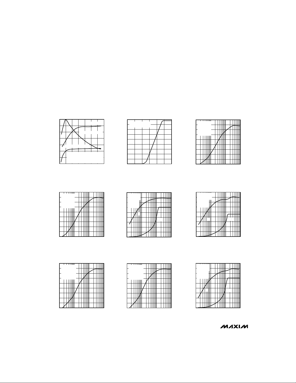
____________________________Typical Operating Characteristics (continued)
(TA = +25°C, unless otherwise noted.)
VPPA AND VPPB OUTPUT POWER
VPPA SHORTED TO VPPB AND
400
MAX781
350
300
250
200
CURRENT (mA)
150
100
CLAMPED TO 11.5V
VPPA + VPPB CURRENT
CONFIGURATION = $FF, $00, $02, $6A,
SYNC = AGND, NO 3OUT LOAD
T1 TURNS RATIO (SECONDARY
TURNS / PRIMARY TURNS) = 3.5
50
4
6 8 10 12 14 16 18
VHI VOLTAGE
BATT INPUT CURRENT
BATT VOLTAGE (V)
14.0
MAX781-02
13.5
13.0
12.5
12.0
11.5
11.0
10.5
DCHG DUTY CYCLE vs. COMP VOLTAGE
90
AT 0% DUTY CYCLE,
80
DCHG = 5OUT
70
60
50
40
VHI VOLTAGE (V)
30
DCHG DUTY CYCLE (%)
20
10
0
0.5 1.0 1.5 2.0 2.5 3.0
0
COMP VOLTAGE (V)
MAX781-04
3OUT OPERATE MODE POWER EFFICIENCY
(FIXED 300kHz SWITCHING FREQUENCY)
100
BATT = 5.5V
90
SYNC = REF
IDLE = 0
80
MODE1 = 1
MODE0 = 0
70
60
50
40
POWER EFFICIENCY (%)
30
20
10
1 10 100 1000
3OUT OUTPUT CURRENT (mA)
MAX781-05
3OUT OPERATE MODE POWER EFFICIENCY
(FIXED 230kHz SWITCHING FREQUENCY)
100
BATT = 5.5V
90
SYNC = AGND
IDLE = 0
80
MODE1 = 1
MODE0 = 0
70
60
50
40
POWER EFFICIENCY (%)
30
20
10
1 10 100 1000
3OUT OUTPUT CURRENT (mA)
3OUT OPERATE MODE POWER EFFICIENCY
(FIXED 300kHz SWITCHING FREQUENCY)
100
BATT = 7.5V
90
SYNC = REF
IDLE = 0
80
MODE1 = 1
MODE0 = 0
70
60
50
40
POWER EFFICIENCY (%)
30
20
10
1 10 100 1000
3OUT OUTPUT CURRENT (mA)
MAX781-06
MAX781-08
3OUT OPERATE MODE POWER EFFICIENCY
(VARIABLE SWITCHING FREQUENCY)
100
BATT = 5.5V
90
SYNC = REF
IDLE = 1
80
MODE1 = 1
MODE0 = 0
70
60
50
40
POWER EFFICIENCY (%)
30
20
10
100
90
80
70
60
50
40
POWER EFFICIENCY (%)
30
20
10
%
1 10 100 1000
3OUT OUTPUT CURRENT (mA)
3OUT OPERATE MODE POWER EFFICIENCY
(FIXED 230kHz SWITCHING FREQUENCY)
BATT = 7.5V
SYNC = AGND
IDLE = 0
MODE1 = 1
MODE0 = 0
1 10 100 1000
3OUT OUTPUT CURRENT (mA)
3OUT OPERATE MODE POWER EFFICIENCY
(VARIABLE SWITCHING FREQUENCY)
450
400
MAX781-12
350
300
250
kHz
200
150
100
50
0
MAX781-07
100
BATT = 5.5V
90
SYNC = AGND
IDLE = 1
80
MODE1 = 1
MODE0 = 0
70
60
50
40
POWER EFFICIENCY (%)
30
SWITCHING FREQUENCY (kHz)
20
10
100
90
80
70
60
50
40
POWER EFFICIENCY (%)
30
20
10
%
1 10 100 1000
3OUT OUTPUT CURRENT (mA)
3OUT OPERATE MODE POWER EFFICIENCY
(VARIABLE SWITCHING FREQUENCY)
BATT = 7.5V
SYNC = REF
IDLE = 1
MODE1 = 1
MODE0 = 0
%
1 10 100 1000
3OUT OUTPUT CURRENT (mA)
kHz
450
400
MAX781-10
350
300
250
200
kHz
150
100
SWITCHING FREQUENCY (kHz)
50
0
450
400
MAX781-11
350
300
250
200
150
100
SWITCHING FREQUENCY (kHz)
50
0
6 _______________________________________________________________________________________
Page 7
PDA/Hand-Held Computer Power Controller
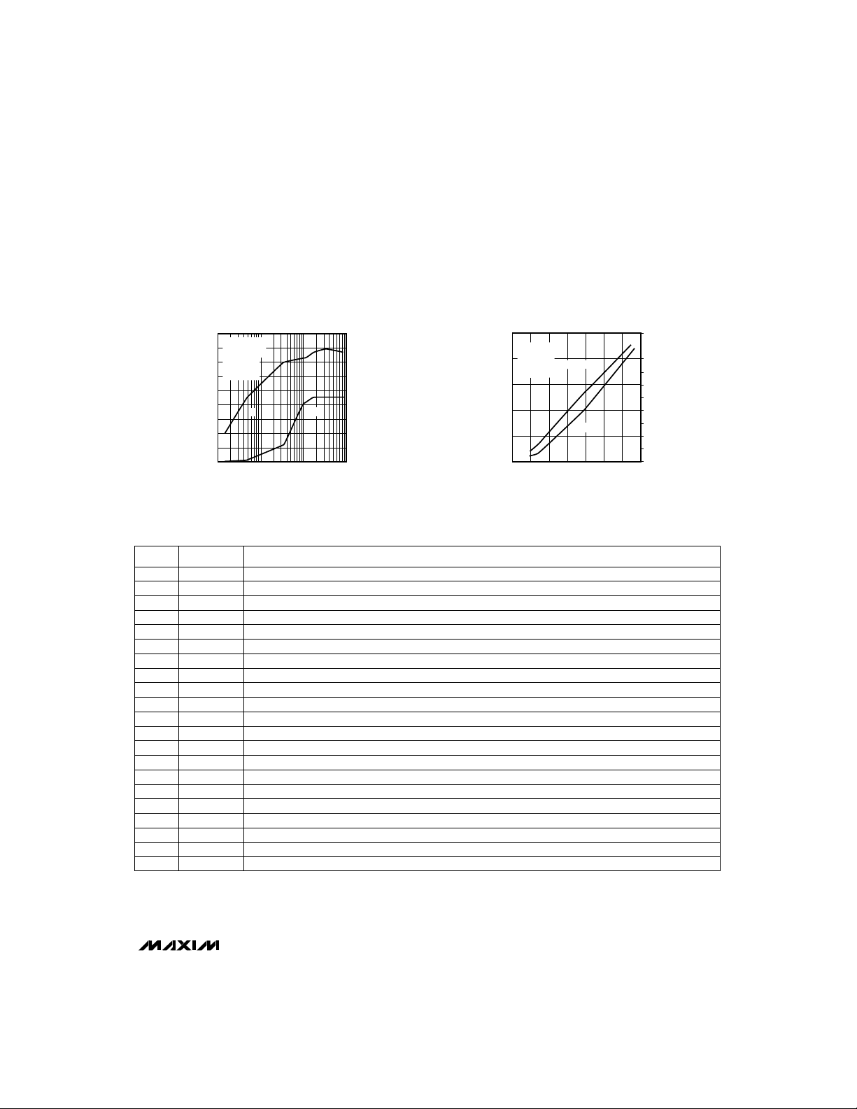
____________________________Typical Operating Characteristics (continued)
(TA = +25°C, unless otherwise noted.)
3OUT OPERATE MODE POWER EFFICIENCY
VARIABLE SWITCHING FREQUENCY
100
BATT = 7.5V
90
SYNC = AGND
IDLE = 1
80
MODE1 = 1
MODE0 = 0
70
60
50
40
POWER EFFICIENCY (%)
30
20
10
%
1 10 100 1000
3OUT OUTPUT CURRENT (mA)
kHz
450
400
MAX781-09
350
300
250
200
150
100
SWITCHING EFFICIENCY (kHz)
50
0
USING THE BATTERY CHARGER TO DRIVE
A CCFL BACKLIGHT ROYER OSCILLATOR
2.5
SYNC = REF
VCHG = 7V
2.0
BATT = VCHG - DIODE DROP
R4 = 0.47Ω
1.5
1.0
0.5
CCFL TUBE CURRENT (mA, rms)
0
0
mV
mA, rms
10 20 30 40 50 60 70
CHG6–CHG0 BITS VALUE
110
100
MAX781-01
90
80
70
60
50
40
30
CSBAT AVERAGE VOLTAGE (mV)
20
10
______________________________________________________________Pin Description
PIN
1–4 GD2–GD5 High-Side Gate-Driver Outputs
5 VPPA VPP-Programming Voltage Output A
6 VHI VPPA, VPPB Linear-Regulator Input Power
7 VPPB VPP-Programming Voltage Output B
8 AGND Analog Ground
9 SYNC Oscillator Frequency Control and Synchronization Input
10 CE Serial-Interface Chip-Enable Input—active high
11 SCLK Serial-Interface Clock Input
12 DOUT Serial-Interface Data Output
13 DIN Serial-Interface Data Input
14 INT Interrupt Output
15 FAST General-purpose open-drain output
16 COMP Battery-Charger Compensation
17 CSBAT Battery-Charger Current-Sense Input
18 5OUT Linear-Regulated +5V Output
19 DCHG Battery-Charger MOSFET Gate-Driver Output
20 PGND Power Ground
21 DLO +3.3V Regulator, Synchronous Rectifier, Gate-Driver Output
22 BST +3.3V Regulator Boost Capacitor Connection (0.1µF to LX)
23 DHI +3.3V Regulator High-Side Gate-Driver Output
24 LX +3.3V Regulator Inductor Connection
NAME FUNCTION
MAX781
_______________________________________________________________________________________
7
Page 8
PDA/Hand-Held Computer Power Controller
_________________________________________________Pin Description (continued)
25 3OUT +3.3V Regulator Feedback Connection and Linear-Regulated + 3.3V Output
26 CS +3.3V Regulator Current-Sense Input
27 SS +3.3V Regulator Soft-Start Capacitor Connection
28 BATT Battery Voltage Input
29 VCHG Charger Voltage Input
MAX781
30 UVLO Undervoltage Lockout Threshold Input
31 REF +2.5V Reference Output
32 AOUT Analog Multiplexer Buffered Output
33 TEMP Analog Multiplexer Input and Battery Sense Input
34 AUXIN Analog Multiplexer Input
35
36 GD1 High-Side Gate-Driver Output
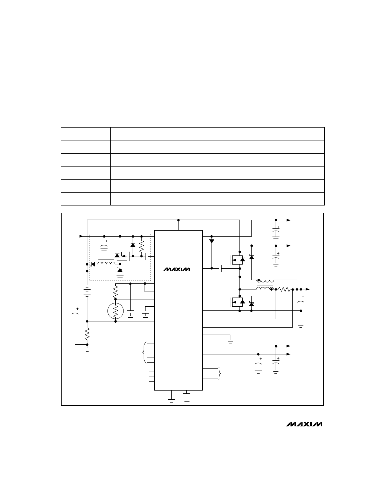
BATTERY
CHARGER
DC INPUT
C10
–S—H—D—N–
D3
R4
Shutdown-Mode Control Input
C14 D1
L1
R8
T
D2
COMPATIBLE
INTERFACE
M3
SPI
SERIAL
R1
C1
BATTERY
CHARGER
SECTION
C3 C2
VCHG
DCHG
REF
SYNC
TEMP
COMP
CSBAT
CE
SCLK
DIN
DOUT
INT
FAST
AUXIN
AOUT
SHDN
MAX781
UVLO SS
C5
5OUT
BATT
BST
DLO
PGND
3OUT
AGND
VPPA
VPPB
GD1
GD5
VHI
DHI
+5V LOW
CURRENT OUTPUT
C12
D7
M1
C7
LX
M2
CS
GATE DRIVERS
FOR POWER
SWITCHING
D6
T1
D5
C8
C11
R7
C9
+14V OUTPUT
PCMCIA 2.0
CARD SLOT
VPPs
C6
+3.3V
OUTPUT
Figure 1. Typical Operating Circuit
8 _______________________________________________________________________________________
Page 9

PDA/Hand-Held Computer Power Controller
MAX781
VCHG
BATT
UVLO
SHDN
AGND
SCLK
DIN
+3.3V LINEAR
REGULATOR
2.5V
REFERENCE
+5V LINEAR
REGULATOR
+3.3V SWITCHING
CHGSTAT
50N
CE
UNDERVOLTAGE
BIAS
GEN
MODE1
MODE0
SERIAL INTERFACE
IDLE
REGULATOR
3VSTAT
AVPP1
INREG
VPP LINEAR
REGULATORS
AVPP0
BVPP1
BVPP0
3OUT
REF
CS3
SS
BST
DHI
LX
DLO
PGND
SYNC
VHI
VPPA
VPPB
INT
DOUT
FAST
MUX_
BATTSTAT
AUXIN
AOUT
TEMP
ANALOG
MULTIPLEXER
Figure 2. MAX781 Block Diagram
_______________________________________________________________________________________ 9
CHG_
BATTERY
CHARGER
CHGON
DCHG
COMP
CSBAT
GATE
DRIVERS
GDON
5
MUXON
37
GDSEL_
5
Page 10

PDA/Hand-Held Computer Power Controller
_______________Detailed Description
Table 1 describes the MAX781’s four modes of operation, and Table 2 shows how to select the desired
mode. MODE1 and MODE0 are the two bits, out of a
total of 32 bits of configuration data, which select the
operational mode. See Table 3 for a complete list of
MAX781
the 32 bits of configuration data.
Table 1. MAX781 Modes of Operation
MODE DESCRIPTION
• Entire chip shut down
Shutdown
Low
Power
Standby
Operate
With –S—H—D—N–pulled up to the battery voltage, the
MAX781 powers on in low-power mode. After powerup, pulling CE high temporaily places the MAX781 into
operate mode and allows data to be shifted into the
internal shift register. As soon as CE goes low, the
MAX781 enters the mode programmed by the MODE1
and MODE0 bits.
• All blocks turned off
• I
< 10µA
Q
• 3OUT, 5OUT, REF off
• Default on power-up
• 3OUT supplies 10mA at +3.3V linear
regulated from BATT
• VPP outputs off (VPPA = VPPB = High-Z)
• Analog multiplexer off (AOUT = High-Z)
• High-side gate drivers off
(GD1 = GD2 = GD3 = GD4 = GD5 = 0V)
• Battery-charging current source off
(DCHG = 5OUT)
• 3OUT supplies 10mA at +3.3V linear
regulated from BATT
• VPP outputs off (VPPA = VPPB = High-Z)
• Analog multiplexer enabled
• High-side gate drivers off
• Battery-charging current source enabled
• Buck switching regulator on
• 3OUT regulated to +3.3V
• VPP outputs enabled
• VHI regulated to +14V
• Analog multiplexer enabled
• High-side gate drivers enabled
• Battery-charging current source enabled
Modes of Operation
Table 2. Operating Modes
–S—H—D—N–
MODE1 MODE0
0 x x
1 1 1
1 1 1 0
1 0 1
1 0 1
1 0 0
1 1 0
CE
x
Shutdown
1
Operate
Low Power (default
on power-up)
1
Standby
0
Low Power
x
Standby
x
Operate
Resulting Mode
Serial Interface
The MAX781 is controlled by 32 bits of configuration
data. These 32 bits must be written, MSB first, into the
MAX781 using a synchronous serial interface. Table 3
describes the function of each bit of configuration data.
To turn the gate drivers on/off, select VPP voltages or
program the analog multiplexer. CE, SCLK, DIN, and
DOUT are the synchronous serial-interface pins. Figure
3 shows an example of the signal timing necessary to
send 32 bits of data to the MAX781. The first six bits
clocked out of DOUT are the status bits, and the
remaining 26 bits clocked out of DOUT should be
ignored. Figure 4 shows the detailed timing requirements of the synchronous serial interface.
To write the last eight bits of the configuration data
without affecting the rest of the configuration bits, clock
eight bits instead of 32 into DIN. This allows the
CHARGE, IDLE, MODE1, MODE0, and VPP control bits
to be updated in only eight serial clock cycles. As the
eight bits are clocked into DIN, the status bits are
clocked out of DOUT. Figure 5 shows an example of
such a quick access. If eight zeros are sent in a quick
access, no configuration data is updated. This allows
the status bits to be read quickly without affecting the
last byte of configuration data.
Status Bits
As the 32 bits of serial-configuration data are written
into the MAX781, 32 bits of data are read out of DOUT.
The first six bits contain status information, and the
remaining 26 bits should be ignored.
BATTINT and BATTSTAT (Table 3) indicate battery status. It is assumed that the battery pack used with the
MAX781 has a thermistor attached to its negative termi-
10 ______________________________________________________________________________________
Page 11

PDA/Hand-Held Computer Power Controller
Table 3. Configuration Data-Bit Assignments
NAME
BIT
*
0
0
0
0
0
0
0
0
0
0
1
0
1
0
0
0
0
0
0
1
0
1
0
1
1
1
1
0
0
0
0
BATTINT
BATTSTAT
3VINT
3VSTAT
CHGINT
CHGSTAT
GDSEL5
GDSEL4
GDSEL3
GDSEL2
GDSEL1
MUX2
MUX1
MUX0
CHG6
CHG5
CHG4
CHG3
CHG2
CHG1
CHG0
50N
FASTON
CHARGE
IDLE
MODE1
MODE0
VPPB1
VPPB0
VPPA1
VPPA0
1 = TEMP pin voltage crossed 0.82* 3OUTR/W31
1 = TEMP > 0.82*3OUT, 0 = TEMP < 0.82*3OUTR30
1 = 3OUT fault detectedR/W29
1 = 3OUT out of regulation, 0 = in regulationR28
1 = VCHG > BATT detectedR/W27
1 = VCHG > BATT, 0 = VCHG < BATTR26
Unused25
1 = GD5 sources from VHI, 0 = GD5 sinks to AGNDW24
1 = GD4 sources from VHI, 0 = GD4 sinks to AGNDW23
1 = GD3 sources from VHI, 0 = GD3 sinks to AGNDW22
1 = GD2 sources from VHI, 0 = GD2 sinks to AGNDW21
1 = GD1 sources from VHI, 0 = GD1 sinks to AGNDW20
Analog multiplexer bit 2W19
Analog multiplexer bit 1W18
Analog multiplexer bit 0W17
Charger current setting DAC bit 6W16
Charger current setting DAC bit 5W15
Charger current setting DAC bit 4W14
Charger current setting DAC bit 3W13
Charger current setting DAC bit 2W12
Charger current setting DAC bit 1W11
Charger current setting DAC bit 0W10
1 = 5OUT linear regulator on, 0 = offW9
1 = FAST sinks current, 0 = FAST open drainW8
1 = DCHG switching current source on, 0 = offW7
1 = Idle regulation, 0 = PWM regulationW6
Operating mode select bit, 1, see Table 2W5
Operating mode select bit, 0, see Table 2W4
VPPB voltage select bit 1, see Table 5W3
VPPB voltage select bit 0, see Table 5W2
VPPA voltage select bit 1, see Table 5W1
VPPA voltage select bit 0, see Table 5W0
MAX781
DESCRIPTIONR/W
* = Power-on reset default state
nal, causing the battery pack to need at least three terminals: BATT+, BATT,- and THERM. The MAX781’s
TEMP pin connects to the battery pack’s thermistor
(Figure 6). Without the battery pack installed, R8 pulls
the MAX781’s TEMP pin up to 3OUT, and BATTSTAT =
1. When the battery pack is inserted, the resistive
divider formed by the thermistor and R8 pulls the TEMP
pin below 3OUT, forcing BATTSTAT = 0. Any transition
of BATTSTAT sets BATTINT. Clear BATTINT by writting
a logic 1 in bit 31 of the serial-configuration data. The
______________________________________________________________________________________ 11
BATTSTAT comparator is disabled in low-power and
shutdown modes, and outputs a logic zero regardless
of the state of its inputs.
3VINT and 3VSTAT indicate the status of the 3OUT
output (+3.3V ±4%). 3OUT is out of regulation when
its output voltage falls below +3.1V. 3VSTAT = 0 when
3OUT is in regulation, and 3VSTAT = 1 when 3OUT is
out of regulation. A rising edge on 3VSTAT sets
3VINT; thus, 3OUT going out of regulation sets 3VINT.
Page 12

PDA/Hand-Held Computer Power Controller
TIME
OUTPUT FROM CPU
INPUT TO MAX781
OUTPUT FROM CPU
INPUT TO MAX781
CE
SCLK
MAX781
OUTPUT FROM CPU
INPUT TO MAX781
INPUT TO CPU
OUTPUT FROM MAX781
DATA CLOCKED INTO MAX781
ON RISING EDGE OF SCLK
DIN
DATA CLOCKED OUT OF MAX781
ON FALLING EDGE OF SCLK
DOUT
Figure 3. Serial Configuration Data Example Timing
CE
SCLK
DOUT
DIN
t
CSO
t
CSS
t
DV
Figure 4. Detailed Timing Diagram
CE
SCLK
BATTINT 3VINT VPPA1 VPPA0
BATTSTATBATTINT 3VINT
XXX XXX XXX
• • •
t
CP
t
CH
t
CSH
• • •
t
DS
t
DH
t
CL
• • •
t
DO
t
TR
• • •
TIME
t
CSW
t
CS1
DIN
DOUT
CHARGE MODE1 MODE0IDLE VPPA1VPPB0VPPB1 VPPA0
BATTSTAT 3VSTAT CHGINT CHGSTATBATTINT 3VINT
XXX XXX XXX
Figure 5. Quick-Access Example Timing
12 ______________________________________________________________________________________
Page 13

PDA/Hand-Held Computer Power Controller
The 3VSTAT comparator is disabled in the low-power,
standby, and shutdown modes, and outputs a logic
zero regardless of the state of its inputs. The MAX781
serial-interface outputs are powered from 3OUT. If
3OUT is short circuited to ground, then neither DOUT
nor INT will be able to source current.
CHGINT and CHGSTAT indicate the status of the
charging voltage applied to VCHG. The MAX781 powers itself from either BATT or VCHG, whichever has the
higher voltage. CHGSTAT = 0 when BATT is approximately 200mV greater than VCHG. CHGSTAT = 1
when BATT falls below VCHG plus approximately
200mV. Any transition on CHGSTAT sets CHGINT.
The CHGSTAT comparator is disabled only in shutdown mode.
At power-up, BATTINT is set if the charger is not connected, CHGINT is set if the charger is connected.
Table 4. Status Detection in the Four Operating
Modes
Low
Power
R
TEMP
MODE
Standby
Enabled
Enabled
Enabled
BATT
3OUT
TEMP
Operate
Enabled
Enabled
Enabled
83kR8
STATUS
BIT
BATTSTAT Disabled Disabled
3VSTAT Disabled Disabled
CHGSTAT Disabled Enabled
BATT+
Shutdown
BATTERY
PACK
THERM
T
The INT pin outputs the logical OR of the BATTINT,
3VINT, and CHGINT status bits. The INT pin generates
an interrupt on the CPU that controls the MAX781.
Supply and Reference
5OUT outputs +5V, linear regulated from either BATT or
VCHG, in all modes except shutdown. 5OUT can
source up to 25mA. Power comes from BATT as long
as the BATT voltage is greater than the VCHG voltage.
When the VCHG voltage exceeds BATT, VCHG supplies the 5OUT linear regulator.
The MAX781’s internal circuitry is powered from 5OUT.
When the DLO pin drives high, it sources current from
5OUT. The DOUT and INT pin output drivers are powered from 3OUT. If an external 5V supply is available
and connected to the 5OUT pin, the 5OUT linear regulator can be disabled by clearing the 5ON bit. If 5ON is
cleared without an external +5V supply connected to
5OUT, or if 5OUT is shorted to ground, the MAX781
internal registers will be cleared to their power-on state.
3.3V Output
3OUT outputs +3.3V in all modes except for shutdown.
In low-power and standby modes, 3OUT is linear regulated from either BATT or VCHG, whichever has the
higher voltage. In operate mode, the switch-mode
buck (step-down) converter is activated to regulate
3OUT to 3.3V. In operate mode, the 3OUT linear regulator is off.
WRITING A "1" TO BATTINT
CLEARS THE FLIP FLOP
TO ANALOG MULTIPLEXER
COMPARATOR DISABLED IN
LOW-POWER MODE; OUTPUTS "0"
REGARDLESS OF STATE OF INPUTS
CLR
D
>
>
BATTINT
Q
BATTSTAT
MAX781
BATT-
R4
Figure 6. BATTINT, BATTSTAT Status Circuitry
______________________________________________________________________________________ 13
1µF
AGND,
PGND
14.1k
MAX781
402k
Page 14

PDA/Hand-Held Computer Power Controller
DHI high-side drives an external N-channel power
MOSFET, M1. Inside the MAX781, the DHI driver is
well-isolated so it can be powered separately from the
rest of the chip. The DHI driver is powered by current
that flows into BST and out of LX. Thus, BST is the
“power” connection and LX is the “ground” connection
for the DHI driver. An internal level shifter allows the
MAX781 internal circuitry to communicate with the DHI
MAX781
driver.
R
, connected from CS to 3OUT, senses current in
SENSE
the primary of transformer T1. With no load on VHI, the
primary of T1 can be treated as the inductor in a current-mode buck converter. R
the primary and turns off M1 when the current limit is
reached. The current limit is adjusted to ensure that
3OUT stays at 3.3V. With M1 off, M2 stays on until the
voltage on R
current limit that protects the output in the event 3OUT
is short circuited to ground. When the voltage from
3OUT to CS reaches 100mV, M1 is turned off whether
or not 3OUT is in regulation.
A capacitor (C5) on the soft-start (SS) pin allows the
current limit to slowly ramp up when power is first
applied. A 4µA current source from 3OUT feeds the SS
pin. The ramp time to full current limit is approximately
1ms for every nanofarad of capacitance on SS, with a
minimum value of 10ns. Once the SS pin reaches 3.3V,
the maximum peak current is available.
UVLO prevents the buck regulator and battery charger
from switching if 5OUT is out of regulation. The voltage
on UVLO is compared to REF. If UVLO is greater than
REF, the buck regulator and battery charger will function normally. With UVLO less than REF, the buck regulator and battery charger stay off and the low-power
mode linear regulator supplies 3OUT, whether or not
operate mode has been set. Tying UVLO to AGND
allows an internal resistive divider to feed the UVLO comparator, preventing operation of the buck regulator and
battery charger for 5OUT voltages less than approximately
4.35V (see the
The MAX781 3.3V buck regulator is similar to the 3.3V
buck regulator on the MAX783. For further information,
refer to the MAX783 data sheet
reaches zero. There is an absolute
SENSE
Electrical Characteristics
detects current in
SENSE
).
Idle Regulation vs. PWM Regulation
In operate mode, 3OUT can be regulated using pulseskipping (Idle-Mode™ regulation) or pulse-width-modulation (PWM) regulation. The IDLE bit selects the
regulation scheme used for load current below about
25% of current limit.
Idle-Mode™ regulation pulses M1 until 25% of the
absolute current limit is reached, at which point M1
turns off. M1 does not turn on again until 3OUT falls
below 3.3V. This scheme improves light-load efficiency
by minimizing the number of times M1 needs to be
turned on to keep 3OUT in regulation. However, the
operating frequency varies with load. At load currents
above 25% of current limit, the regulator uses resonant
frequency PWM regulation independent of the idle bit.
PWM regulation turns M1 on at a constant frequency
and modulates M1’s duty cycle to maintain the current
required to keep 3OUT in regulation. The switching frequency remains constant regardless of the load current. Operating with a constant frequency results in
lower amplitude and more easily filtered output ripple.
The SYNC pin either sets the internal switching frequency or synchronizes the MAX781 to an external
oscillator. Tying SYNC to REF sets a switching frequency of 300kHz. Tying SYNC to 5V or AGND sets a
230kHz switching frequency. Driving SYNC with an
external oscillator synchronizes the PWM switching with
the external oscillator.
VPP Regulator
VPPA and VPPB linear regulate VHI down to
0V/+3.3V/+5V/+12V for use as a PCMCIA VPP voltage.
The VPPB0, VPPB1, VPPA0, VPPA1 bits control the
VPPB and VPPA output voltage. Programming VPPA or
VPPB to 0V shuts off the linear regulator and saves quiescient supply current. Table 5 shows how to program
the VPPA and VPPB control bits.
During the flyback phase of the buck converter (DLO
on), VHI loads 3OUT. As long as DLO is on, power can
be supplied to VHI. When 3OUT has a light load, DLO
may not stay on long enough to supply power to VHI.
To prevent VHI from sagging, an internal comparator
checks VHI. If VHI sags below 12.8V, DLO is turned on
for 1µs to provide power to VHI, regardless of the voltage on RSENSE. Power can only be delivered to VHI in
operate mode when the buck switching regulator is
active.
The VHI pin includes an overvoltage clamp that sinks
current if VHI exceeds 19V.
This prevents the parasitic capacitance in transformer
T1 from causing the VHI voltage to climb without limit.
™Idle-Mode is a trademark of Maxim Integrated Products.
14 ______________________________________________________________________________________
Page 15

PDA/Hand-Held Computer Power Controller
Table 5. VPPA and VPPB Control Bits
VPPA1
0 0
0 1
1 0
1 1
VPPB1 VPPB0
0 0
0
1
1 1 3.3
VPPA0
1
0
VPPA Voltage (V)
0
5
12
3.3
VPPB Voltage (V)
0
5
12
Gate Drivers
GD1 through GD5 are gate-driver outputs that highside drive external N-channel power MOSFETs. Loads
connected to 3OUT can be connected or disconnected
by using the circuitry shown in Figure 7. Clearing
GDSEL1 (GDSEL1 = 0) causes GD1 to sink up to
450µA to AGND. Setting GDSEL1 (GDSEL = 1) causes
GD1 to source up to 10µA from VHI. GD2–GD5 operate the same way. VHI is active (i.e., regulated to at
least 12.8V) only in operate mode, so the gate drivers
also only function in operate mode. GDSEL1 defaults
to a 1 on power-up. GDSEL2 through GDSEL5 default
to 0 on power-up.
FAST is a general-purpose output pin that sinks current
when FASTON = 1 and goes open drain when FASTON
= 0. FAST can be pulled up to any voltage up to 19V.
To use FAST as a general-purpose 3.3V logic output,
pull it up to 3OUT with a 100kΩ resistor. FAST may be
used to pull the gate of M3 down to connect the battery
to the input supply. The MAX781 does not limit the battery current when FAST is used in this way.
...TO REST OF 3OUT CIRCUIT
3OUT
GD_
MAX781
NEEDS TO BE TURNED
AGND
...TO REST OF AGND CONNECTIONS
Figure 7. Using the Gate Drivers for High-Side Load Switching
N-CHANNEL
POWER MOSFET
3.3V LOAD THAT
ON/OFF
The battery charger is a voltage-mode average current
Battery Charger
regulator. Figure 8 shows a functional diagram of the
battery charger circuitry. The GMAMP is a transconductance amplifer with approximately 62dB of openloop DC gain. Set the GMAMP bandwidth with the
capacitor on COMP.
GMAMP bandwidth in hertz = gm / C
where gm = 0.0006 mho (mho = 1/Ω) and C = capacitance on COMP in farads.
Average the current-sense signal by setting the
GMAMP bandwidth much lower than the battery-charger switching frequency. The voltage output of the
GMAMP at COMP is converted to a duty cycle, which is
driven out of DCHG.
Serial-configuration bits CHG6–CHG0 set the average
current level. When CHG6–CHG0 are all set (1111111),
CSBAT is regulated to an average of 200mV. When
CHG6–CHG0 equals binary 0111111, CSBAT is regulated to an average of 100mV.
CHG6–CHG0
DACOUT
(0mV TO 200mV)
GMAMP
CSBAT
Figure 8. Battery-Charger Block Diagram
7-BIT DAC
AT 0% DUTY CYCLE, DCHG = 5OUT
VOLTAGE TO
DUTY CYCLE
CONVERTER
5OUT
DCHG = 5OUT
EXTERNAL SWITCH OFF
DCHG = AGND
EXTERNAL SWITCH ON
PGNDCOMP
DCHG
Analog Multiplexer
The MAX781’s built-in buffered analog multiplexer
selects one of eight different signal sources to be output from the AOUT pin. Figure 9 shows the analog multiplexer circuitry. The AOUT buffer amplifier is disabled
in the shutdown and low-power modes, leaving the
89.7kΩ resistor to pull AOUT down to ground. Program
the MUX0, MUX1, MUX2 bits in the serial-configuration
data to select the analog multiplexer channel (Table 6).
Resistive dividers in the signal paths scale the channels to ensure that AOUT is scaled to REF. The AOUT
buffer amplifier can sink or source 1mA.
MAX781
______________________________________________________________________________________ 15
Page 16

PDA/Hand-Held Computer Power Controller
Table 6. Analog Multiplexer Channel Selection
MUX2
MAX781
0
0
AUXIN
REF
VPPB
VPPA
TEMP
BATT
5OUT
3OUT
MUX0
MUX1
MUX2
Figure 9. Analog Multiplexer Circuitry
A0
A1
A2
MUX1
3-to-8
DECODER
11
11
01
10
10
0
0
498.4k
116k
498.4k
116k
500k
125k359k
200k
183.3k
150k
300k
Y0
Y1
Y2
Y3
Y4
Y5
Y6
Y7
MUX0
1
0
1
0
1
0
1
0
AOUT
OUTPUTS
AUXIN/1.5
REF
VPPB/5.3
VPPA/5.301
TEMP/1.5
BATT/5
5OUT/2.2
3OUT/1.5
89.7k
AOUT
_Component Selection and Layout
3.3V Output
Input and Output Bypass Capacitors
Capacitor C15 ensures that the buck regulator has a
low AC-impedance power source. C15’s root mean
square ripple-current rating must be greater than 0.5 x
(maximum power output capability of the system) /
3.3V. Capacitor C6 keeps 3OUT output ripple low and
stabilizes the regulation loop. C15 and C6 must have
low equivalent series resistance (ESR), preferably with
less than 0.2Ω of ESR at 200kHz. Tantalum capacitors
typically have the lowest ESR. C15’s ground connection must be as close as possible to C6’s ground connection; ideally, the two capacitors will be grounded at
the same point. The MAX781’s AGND pin should only
connect to system ground at the ground connection of
C15 and C6. If the PC board has a ground plane, a
separate trace should directly connect AGND to the
ground connections of C15 and C6. Likewise, the
BATT pin should only connect to the battery at C15’s
positive terminal.
The capacitance and ESR of C6 determine loop stability. To ensure loop stability, the minimum capacitance
and maximum ESR values are:
C6 > 2.5V / (3.3V x R7 x 2 x p x GBWP)
with C6 specified in Farads, R7 specified in ohms,
GBWP = gain bandwidth product of 60,000Hz, and:
C6 ESR < (3.3V x R7) / 2.5V
with C6 ESR specified in ohms, and R7 specified in
ohms.
In order to achieve the required low ESR, it may be
appropriate to select a value greater than the minimum
for C6, or to construct a composite C6 by paralleling
several smaller capacitors.
Current-Sense Resistor
Current-sense resistor R7 sets the maximum peak current through power switch M1 and the primary of transformer T1. The MAX781’s maximum peak current limit
is 120mV / R, where R is the minimum possible resistance for R7, and 120mV is the maximum electrical
specification for the current-limit threshold. For example, selecting a 0.082Ω ±1% resistor for R7 yields a
maximum peak current limit of 120mV / 0.082Ω x 0.99 =
1.478A. The maximum peak current limit must be less
than or equal to the maximum allowed continuous DC
current through either M1 or the primary of T1.
R7 also determines how much power 3OUT, VPPA, and
VPPB can deliver. The current-limit threshold can be
as small as 80mV and, using a 0.082Ω ±1% resistor,
16 ______________________________________________________________________________________
Page 17

PDA/Hand-Held Computer Power Controller
R7 can be as large as 0.082Ω x 1.01 = 0.0828Ω, yielding a minimum peak current limit of 80mV / 0.0828Ω =
0.966A.
Use the spreadsheet in Listings 1 and 2 to calculate the
power available at 3OUT as a function of the currentsense resistor choice.
Listing 1. Spreadsheet for Calculating 3OUT
Current Capability
Parameter Min Max Units
(Cell A1) (Cell B1) (Cell C1)
Current-Limit Threshold 80 120 mV
Current Sense R7 81 83 mΩ
Current Limit 0.964 1.481 A
Switching Frequency 270 340 kHz
Switching Period 2.941 3.704 µs
T1 Primary Inductance 16 24 µH
3OUT Regulation Point 3.170 3.430 V
BATT Input Range 5.000 17.500 V
(Cell A10)
Current Limit 0.964 A
Switching Period 3.704 µs
T1 Primary Inductance 16 µH
3OUT 3.430
BATT 17.500
VHI Load Current 60 mA
T1 Turns Ratio 3.5
T1 Coupling Loss 80 %
(Cell A20)
T1 Ripple Current 0.638 A
T1 Continuous Current 0.325 A
3OUT Current, No VHI load 0.645 A
VHI Load Power 0.926 W
3OUT Guaranteed Current 0.307 A
(Cell A26) (Cell B26) (Cell C26)
Listing 2. Calculating 3OUT Current-Capability
Formulas
B4: +B2/C3
C4: +C2/B3
B6: 1/C5*1000
C6: 1/B5*1000
B12: +B4
C13: +C6
B14: +B7
C15: +C8
C16: +C9
C21: @MIN(+C15/C16*C13*(C16-C15)/B14,B12)
C22: +B12-C21
C23: @IF(C22=0,0.5*(B14/1000000)*C21^2*1000000/
C13/C15,C22+C21/2)
C24: +C15*(C18+1)*C17/1000
C25: +C23-C24/(C19/100)/C15
R7 must have as little series inductance as possible
and be as physically small as possible. 3OUT and CS3
need to Kelvin sense R7. A pair of traces running in
parallel should leave 3OUT and CS3 and diverge only
when they meet R7. Minimize the distance between
R7 and the positive terminal of C6.
Power MOSFETs
M1 and M2 must be logic level, low r
DS(ON)
, N-channel
power MOSFETs. M1’s drain should be as close as
possible to C15’s positive terminal and M2’s source
should be as close as possible to C15’s ground connection point.
Transformer T1
T1’s primary inductance must be between 10µH and
100µH. The peak current allowed through the primary
with the secondary open circuited must be greater than
the worst-case peak current set by R7. T1’s turns ratio
(number of turns on secondary / number of turns on primary) should be 3.5. If VHI rises up to 20V when 3OUT
is loaded in operate mode, T1 may have too much
interwinding capacitance. Minimize interwinding
capacitance to prevent energy waste in the VHI clamp
(which clamps VHI to 19V to protect the MAX781).
__________Applications Information
Table 7 shows the targets for a typical design requirement. Since both PCMCIA slots will not be programmed at the same time, VPPA and VPPB will never
be at +12V at the same time; thus the worst case for
power consumption is when both 3.3V and VPPA or
VPPB is fully loaded.
Total power consumption = (max 3OUT voltage) x (max
3OUT load current) + (VHI voltage) x (max VPP or load
current) / (transformer efficiency).
Design Example
MAX781
______________________________________________________________________________________ 17
Page 18

PDA/Hand-Held Computer Power Controller
Table 7. Specifications for a Typical Design
PARAMETER
Input Power
3.3V Output
MAX781
Current
VPPA Output
Current
VPPB Output
Current
Charge Current
VPPA and VPPB are linear regulated from VHI, so the
power consumed by loads on VPPA or VPPB equals
the VHI voltage times the load current. Barring a
Schottky diode drop, VHI equals the 3OUT voltage x (1
+ turns ratio). With the specifications of Table 7 and
an 80% transformer efficiency, the total power consumption works out to 2.037W; thus the average current through the primary of T1 is 594mA. The peak
current through the primary of T1 will depend on the
minimum primary inductance. As a rule of thumb, the
peak current will be about 1.5 times the average current. For an average current of 594mA, the peak current would be about 900mA. To achieve a 900mA peak
current, select R7 to be 80mV / 900mA = 0.088Ω. The
closest comercially available value would be 0.082Ω
±1%. The spreadsheet in Listing 1 calculates how high
a guaranteed output current can be, given commercially available component values, and taking component
tolerances into account.
Table 8 shows the electrical specifications for a transformer that meets the requirements of Listing 1.
Power MOSFETs M1 and M2 should have an on-resistance at logic-level gate drive (r
DESIGNATION
5 NiCD cells
15V DC adapter
+12V output when
programming flash
memory in Slot A
+12V output when
programming flash
memory in Slot A
Digitally
programmable
DS(ON)
MIN
MAX
5
17.5
300
60
60 mA
0
1
at VGS= 4.5V)
UNITS
V
mA
mA
A
Table 8. Dale Electronics M/N LPE-6562-A070
Specifications
PARAMETER
Primary Inductance 20
Leakage Inductance
(at 0.1V
Primary Continuous
DC Current
Primary DC Resistance
Secondary DC Resistance
Turns Ratio
(secondary/primary)
RMS
, 100kHz)
of the same order as T1’s primary DC resistance. The
Siliconix Si9955DY dual N-channel MOSFET satisfies
this requirement with a 0.2Ω maximum on-resistance
per device.
Table 9 lists the bill of materials for an example circuit
that fulfills the requirements of Table 7.
MIN
16
TYP
3.5
MAX
24
2.6
0.075
0.51
UNITS
µH
µH0.03
A
Ω
Ω
Driving a CCFL Backlight Royer Oscillator
The digitally adjustable current from the battery charger
can be used to drive a Royer oscillator. The Royer
oscillator is a resonant circuit fed by a constant current.
The root mean square current out of the secondary
winding of the Royer transformer is proportional to the
current fed into the center tap of the Royer transformer.
Figure 10 shows the application circuit. The diode from
VCHG to BATT keeps BATT from dropping too far
below 5OUT, which causes excess supply current.
Figure 11 shows how the programmed current corresponds to the CCFL root mean square tube current.
The NPN transistor connected to COMP and the zener
diode protects the transformer from an open-tube condition by shutting off the Si9953DY if pin 2 of the
CTX110606 exceeds 0.6V + 10V + 0.6V. This limits the
voltage on the secondary to 11.2 x 171 x 2 = 3830.4V
peak-to-peak = 1354V
, which is well within the
RMS
CTX110606 maximum secondary voltage specification
of 2010V
RMS
.
18 ______________________________________________________________________________________
Page 19
PDA/Hand-Held Computer Power Controller
Table 9. Design Example Bill of Materials
SYMBOL
T1 M/N LPE-6562-A070
L1 CDR125-470
M1, M2 Si9955DY
M3 Si9953DY
R1
R4
R7
R8
C1
C2
C3
C5
C6 195D127X06R3R2T
C7
C8
C9
C10 195D226X0025R2T
C11
C12
C14 195D226X0025R2T
D1 CMPD4150
D2 EC10QS03
D3 EC15QS03
D5 EC10QS03
D6 EC10QS05
D7 CMPD4150
transformer
47µH, 1.5A IDC inductor
N-Channel MOSFETs
P-Channel MOSFET
100kΩ, ±20% resistor
0.2Ω, ±1% resistor
0.082Ω, ±1% resistor
10kΩ, ±1% resistor
0.1µF, 20V capacitor
0.33µF, 6V capacitor
1µF, 6V capacitor
0.01µF, 6V capacitor
120µF, 6.3V capacitor, 0.09Ω ESR at 100kHz
0.1µF, 10V capacitor
1µF, 16V capacitor
1µF, 16V capacitor
22µF, 25V capacitor
2.2µF, 25V capacitor
1µF, 6V capacitor
22µF, 25V capacitor
20V 1N4150 type diode
20V Schottky diode
20V Schottky diode
20V Schottky diode
50V Schottky diode
20V 1N4150 type diode
DESCRIPTION
PART No.
MAX781
MANUFACTURER
Dale
Sumida
Siliconix
Siliconix
IRC
IRC
Sprague
Sprague
Sprague
Central
Nihon
Nihon
Nihon
Nihon
Central
Table 10. Component Suppliers
SUPPLIER
(516) 435-1110Central Semiconductor
(407) 241-7876Coiltronics
(605) 665-9301Dale
(213) 772-2000IRC
Nihon
Rep: Quantum Marketing
Siliconix
Wilhelm Westerman
Rep: Inter-Technical Group
Zetex
______________________________________________________________________________________ 19
Japan 81-3-3494-7411
USA (805) 867-2555
(800) 554-5565
(708) 956-0666Sumida
Germany 0621-408012
USA (914) 347-2474
USA (516) 543-7100
UK 061-627-4963
PHONE
FAX
(516) 435-1824
(407) 241-9339
(605) 665-1627
(213) 772-9028
81-3-3494-7414
(805) 867-2698
(408) 970-3950
(603) 224-1430(603) 224-1961Sprague
(708) 956-0702
0621 403538
(914) 347-7230
(516) 864-7630
061-627-5467
Page 20
PDA/Hand-Held Computer Power Controller
MAX781
MAX781
BATT
VCHG
COMP
DCHG
CSBAT
0.1µF
CMPD4448
0.33µF
10k
CMPT3904
CMPD4448
22µF
20V
CMPZ5240B
10k
CMPD4448
Si9953DY
CTX150-4
EC10QS02L
15pF 2kV
2
1
MKS01-SMD
CCFL
FMMT619
M1 DRAIN
CCFL
CTX110606
2345
710Ω
0.1µF
0.47Ω
10
FMMT619
AGND
NOTE: SEE TABLE 10 FOR COMPONENT SUPPLIER INFORMATION.
CM = CENTRAL SEMICONDUCTOR
CT = COILTRONICS
EQ = NIHON INTER ELECTRIC CORP.
FM = ZETEX
MK = WILHELM WESTERMANN
Figure 10. Digitally Adjustable CCFL Backlight Circuit
20 ______________________________________________________________________________________
Page 21

PDA/Hand-Held Computer Power Controller
Interfacing the MAX781 to an
IBM Compatible PC
Figure 1 shows the MAX781 typical operating circuit.
On power-up, with 4.8V < BATT < 18V and CE = SCLK
= DIN = 0V, the MAX781 is in low-power mode. 3OUT
outputs +3.3V linear regulated from BATT, and REF
outputs +2.5V. INT should output a 3.3V logic high.
Neither DHI nor DLO should be switching. Serial data
must be sent to the MAX781 in order to change modes.
The parallel printer interface on a personal computer
can be used to send serial control data to the MAX781.
Listing 3 shows a simple Microsoft Quick Basic program for communicating with the MAX781 over the
LPT1 parallel interface port.
MAX781
______________________________________________________________________________________ 21
Page 22
PDA/Hand-Held Computer Power Controller
Listing 3. MAX781 Control Program in QBasic
MAX781
22 ______________________________________________________________________________________
Page 23
PDA/Hand-Held Computer Power Controller
TOP VIEW
GD2
GD3
GD4
GD5
VPPA
VHI
VPPB
AGND
SYNC
SCLK
DOUT
DIN
FAST
COMP
CSBAT
5OUT
___________________Chip Topography__________________Pin Configuration
GD4
VHI
DIN
INT
CE
GD5 GD3 GD1
FAST
COMP
36
1
2
3
4
5
MAX781
6
7
8
9
CE
10
11
12
13
INT
14
15
16
17
18
GD1
SHDN
35
AUXIN
34
TEMP
33
AOUT
32
REF
31
30
UVLO
VCHG
29
28
BATT
27
SS
26
CS
3OUT
25
LX
24
23
DHI
BST
22
DLO
21
PGND
20
19
DCHG
VPPA
VPPB
AGND
SYNC
SCLK
DOUT
SSOP
GD2 SHDN
DCHG
5OUT
0.152"
(3.861mm)
TEMP
AUXIN
DLOCSBAT
PGND BST
AOUT
REF
UVLO
VCHG
BATT
0.219"
(5.563mm)
SS
CS
3OUT
LX
DHI
MAX781
TRANSISTOR COUNT: 2661
SUBSTRATE CONNECTED TO AGND.
______________________________________________________________________________________ 23
Page 24
PDA/Hand-Held Computer Power Controller
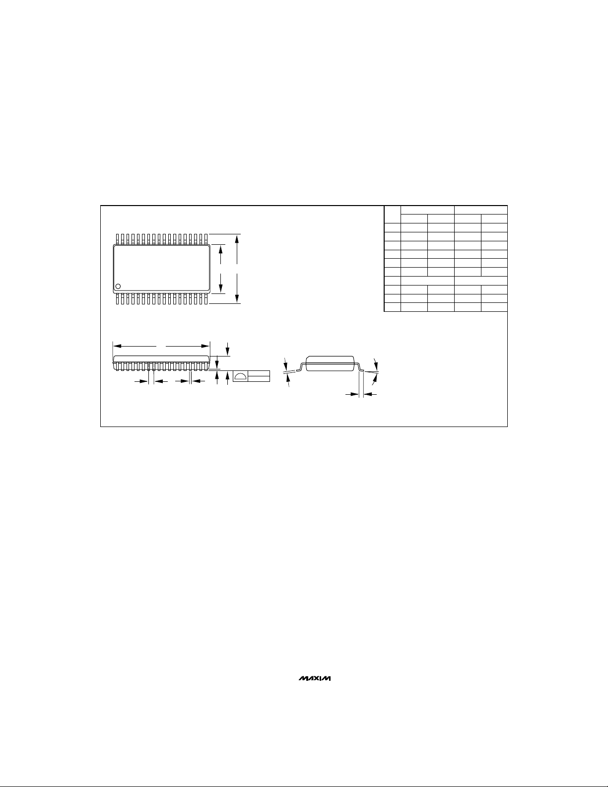
________________________________________________________Package Information
INCHES MILLIMETERS
DIM
MAX781
A
A1
B
C
HE
D
E
e
H
L
α
MIN
0.094
0.004
0.011
0.009
0.604
0.292
0.398
0.020
0˚
MAX
0.104
0.011
0.017
0.012
0.610
0.298
0.416
0.035
8˚
MIN
2.39
0.10
0.30
0.23
15.34
7.42
0.80 BSC0.032 BSC
10.10
0.51
0˚
MAX
2.64
0.28
0.44
0.32
15.49
7.57
10.57
0.89
8˚
21-0032A
D
α
A
0.127mm
0.004in.
A1
e
B
C
L
36-PIN PLASTIC
SHRINK
SMALL-OUTLINE
PACKAGE
Maxim cannot assume responsibility for use of any circuitry other than circuitry entirely embodied in a Maxim product. No circuit patent licenses are
Maxim cannot assume responsibility for use of any circuitry other than circuitry entirely embodied in a Maxim product. No circuit patent licenses are
implied. Maxim reserves the right to change the circuitry and specifications without notice at any time.
implied. Maxim reserves the right to change the circuitry and specifications without notice at any time.
24
__________________Maxim Integrated Products, 120 San Gabriel Drive, Sunnyvale, CA 94086 (408) 737-7600
24
__________________Maxim Integrated Products, 120 San Gabriel Drive, Sunnyvale, CA 94086 (408) 737-7600
© 1994 Maxim Integrated Products Printed USA is a registered trademark of Maxim Integrated Products.
© 1994 Maxim Integrated Products Printed USA is a registered trademark of Maxim Integrated Products.
 Loading...