

Page 1
________________General Description
The MAX769 is a complete buck/boost power supply
and monitoring system for two-way pagers or other lowpower digital communications devices. Few external
components are required. Included on-chip are:
• An 80mA output, synchronous-rectified, buck/boost
DC-DC converter with a digitally controlled +1.8V to
+4.9V output. The DC-DC converter is unique, since
it provides a regulated output for battery inputs that
are both less than and greater than the output voltage, without using transformers.
• Three low-noise linear-regulator outputs
• Three DAC-controlled comparators for software-
driven, 3-channel A/D conversion
• SPI™-compatible serial interface
• Reset and low-battery (LBO) warning outputs
• Charger for NiCd/NiMH, lithium battery, or storage
capacitor for RF PA power or system backup
• Two 1.8Ω (typical), serial-controlled, open-drain
MOSFET switches for beeper or vibrator drive
An evaluation kit for the MAX769 (MAX769EVKIT) is
available to aid in design and prototyping.
____________________________Features
♦ Regulated Step-Up/Step-Down Operation
♦ 80mA Output from 3 Cells
♦ 85% Efficiency
♦ 13µA Idle Mode™ (coast) Current
♦ Selectable Low-Noise PWM or Low-Current PFM
Operation
♦ PWM Operating Frequency Synchronized to
Seven Times an External Clock Source
♦ Operates at 270kHz with No External Clock
♦ Automatic Backup-Battery Switchover
________________________Applications
Two-Way Pagers
GPS Receivers
2 or 3-Cell Powered, Hand-Held Equipment
MAX769
2 or 3-Cell, Step-Up/Down,
Two-Way Pager System IC
________________________________________________________________
Maxim Integrated Products
1
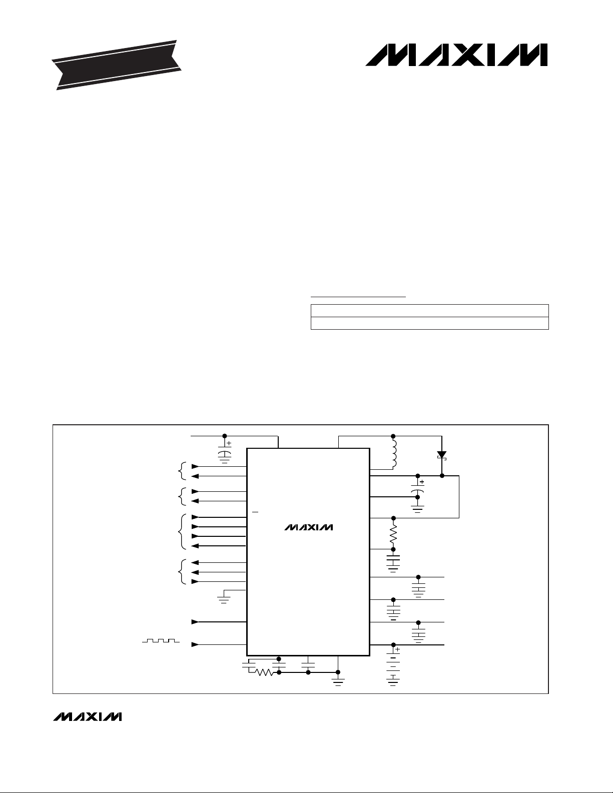
MAX769
INPUT
2 OR 3 AA ALKALINE BATTERIES
1.5V TO 5.5V
BATT
LX2
OUT
PGND
REG2IN
OFS
REG2
OUTPUT 2
2.85V ANALOG
LOW-BATTERY
IN/OUT
REJECT
IN/OUT
SERIAL
I/O
1.8Ω
DRIVERS
A/D
INPUT
OPTIONAL
OUTPUT 1
3V LOGIC
OUTPUT 3
1V RECEIVER
TO RF PA
NiCd
BATTERY OR
STACK
REG1
REG3
NICD
AGNDREFFILT
LBI
LBO
RSIN
RSO
CS
SCL
SD1
SD03
DR1
DR2
DR2IN
DRGND
CH0
SYNC
LX1
STORAGE
CAPACITOR
___________________________________________________Typical Operating Circuit
19-4771; Rev 1; 10/98
PART
MAX769EEI -40°C to +85°C
TEMP. RANGE PIN-PACKAGE
28 QSOP
Ordering Information
Idle Mode is a trademark of Maxim Integrated Products. SPI is a trademark of Motorola, Inc.
Pin Configuration appears at end of data sheet.
For free samples & the latest literature: http://www.maxim-ic.com, or phone 1-800-998-8800.
For small orders, phone 1-800-835-8769.
EVALUATION KIT MANUAL
FOLLOWS DATA SHEET
Page 2
MAX769
2 or 3-Cell, Step-Up/Down,
Two-Way Pager System IC
2 _______________________________________________________________________________________
ABSOLUTE MAXIMUM RATINGS
ELECTRICAL CHARACTERISTICS
(OUT = 3.0V, BATT = 3.6V, TA= -40°C to +85°C, unless otherwise noted. Typical values are at TA= +25°C.) (Note 1)
Stresses beyond those listed under “Absolute Maximum Ratings” may cause permanent damage to the device. These are stress ratings only, and functional
operation of the device at these or any other conditions beyond those indicated in the operational sections of the specifications is not implied. Exposure to
absolute maximum rating conditions for extended periods may affect device reliability.
BATT, OUT, NICD, LBO, RSO to AGND...................-0.3V to +6V
REG1, REG2, OFS, REF, R2IN to AGND .....-0.3V to (OUT + 0.3V)
SCL, SDO, SDI,
CS, SYNC, FILT, DR2IN,
CH0, LBI, RSIN to AGND......................-0.3V to (REG1 + 0.3V)
REG3 .......................................................-0.3V to (REG2 + 0.3V)
DR1, DR2 to DRGND ...............................-0.3V to (BATT + 0.3V)
PGND, DRGND to AGND......................................-0.3V to +0.3V
LX1 to PGND .............................................-0.3V to (OUT + 0.3V)
LX2 to PGND............................................-0.3V to (BATT + 0.3V)
Continuous Power Dissipation (T
A
= +70°C)
QSOP (derate 8mW/°C above +70°C)..........................640mW
Operating Temperature Range ...........................-40°C to +85°C
Junction Temperature......................................................+150°C
Storage Temperature Range.............................-65°C to +165°C
Lead Temperature (soldering, 10sec).............................+300°C
I
REF
= 0 to 20µA, OUT = 1.8V to 4.9V V-1.5% 1.28 1.5%
TA= +25°C
Reference Voltage
IDR= 120mA
Run or Coast Mode
Ω
1.8 2.8
DR1, DR2 On-Resistance
VDR= 5V nA1 250DR1, DR2 Leakage Current
Charger and Backup Modes off, NICD = 3.6V µA
Incremental supply current when on
REG2, REG3 and CH DAC off, V
OUT
= 2.8V
REG2, REG3 and CH DAC on
Coast Mode
1.2 3
Incremental supply current when on
TA= +25°C
CONDITIONS
TA= -40°C to +85°C
I
SDO
= 100µA mV200SDO Output Low
I
SDO
= -100µA, from REG1 V
V
REG1
- 0.2
SDO Output High
Includes CS, SDI, SCL, DR2IN, and SYNC
V0.4Logic Input Level Low
Includes CS, SDI, SCL, DR2IN, and SYNC
V
V
REG1
- 0.4
Logic Input Level High
3.6
Charger and Backup Modes off, BATT = 0V,
OUT = 0V
µA1.2 3
NICD Input Current, Power Fail
(Note 8)
Logic Input = 0 to 3.3V; includes CS, SDI, SCL,
DR2IN, and SYNC
µA
V1.6 2.0
-1 1
BATT Minimum Start-Up Voltage
(Note 3)
V1.5 5.5
Logic Input Current
NICD Input Current, Standby
(Note 6)
BATT Typical Operating Range
(Note 2)
Incremental supply current when on µA
Backup Mode, NICD = 3.6V, OUT = 3V
50REG2 Supply Current (Note 4)
µA20 40
NICD Input Supply Current, Backup
(Note 7)
µA30CH DAC Supply Current (Note 4)
µA13 25Coast Mode Supply Current (Note 4)
µA875 1350Run Mode Supply Current (Note 4)
µA4 10BATT Supply Current (Note 5)
µA20REG3 Supply Current (Note 4)
UNITSMIN TYP MAXPARAMETER
GENERAL PERFORMANCE
Page 3
MAX769
2 or 3-Cell, Step-Up/Down,
Two-Way Pager System IC
_______________________________________________________________________________________ 3
ELECTRICAL CHARACTERISTICS (continued)
(OUT = 3.0V, BATT = 3.6V, TA= -40°C to +85°C, unless otherwise noted. Typical values are at TA= +25°C.) (Note 1)
%-3.5 3.5
OUT Error, Coast Mode
(Note 11)
%
Coast Mode, OUT = 1.8V to 4.9V
-3.5 3.5OUT Error, Run Mode (Note 12)
Circuit of Figure 2, OUT = 3.0V, BATT = 3.0V
Run Mode, OUT = 1.8V to 4.9V
Circuit of Figure 2, OUT = 3.0V, BATT = 3.0V
CONDITIONS
BATT = 1.6V to 4.5V mV25OUT Line Regulation
I
OUT
= 80mA, C
OUT
= 47µF with ESR < 0.25Ω
mVp-p70OUT Voltage Ripple
LX1, LX2, BATT = 3.0V
Ω
0.9 1.8
LX On-Resistance (Note 14)
ns50
ns50
CS to SCL Hold Time (t
CSH
)
CS to SCL Setup Time (t
CSS
)
ns100SDI Setup Time (tDS)
NMOS
PMOS 1.3 2.6
TA= +25°C, FILT connected to REF kHz210 270 325Frequency, Free-Run
Backup Mode, NICD = 3.3V
f
SYNC
= 38.4kHz
ns100
kHz
CS Pulse Width High (t
CSW
)
268.8
ns70
Frequency, Locked
CS to SDO Disable (tTR)
Ω
f
SYNC
= 38.4kHz, FILT Network = 1nF(22nF + 10kΩ)
kHz±15Jitter (Note 15)
5 10
f
SYNC
= 38.4kHz, FILT Network = 1nF(22nF + 10kΩ)
ms1 25Capture Time (Note 15)
Backup-Regulator
On-Resistance (Note 16)
ns50
0.2V < (OUT - NICD) < 2V, 15mA_CHG = 1
SCL Pulse Width High or Low
(tCH, tCL)
mA
mA80 115
7 25
Output Current, Run Mode
(Note 10)
mA15 40
Current High
Output Current, Coast Mode
(Note 10)
UNITSMIN TYP MAXPARAMETER
0.2V < (OUT - NICD) < 2V, 1mA_CHG = 1 mA0.45 1.5Current Low
OUT = 2.8V, I
OUT
= 20mA, NICD = 3.3V %-3.5 3.5OUT Error, Backup Regulator
50% duty cycle MHz5SCL Maximum Clock Rate
OUT = 3.0V %76 83Maximum LX Duty Cycle
During the inductor charge cycle mA300 350 400LX Switch Current Limit
ns70
ns70
CS to SDO Output Valid (tDV)
SCL to SDO Output Valid (tDO)
ns50SDI Hold Time (tDH)
I
OUT
= 1mA to 80mA, Run Mode mV25OUT Load Regulation
Coast or Run Mode, OUT = 1.8V to 4.9V mV30 100 170OUT DAC Step Size (Note 13)
SERIAL-INTERFACE TIMING SPECIFICATIONS (Note 9)
DC-DC CONVERTER
PHASE-LOCKED LOOP (PLL)
NICD CHARGER
Page 4
V
MAX769
2 or 3-Cell, Step-Up/Down,
Two-Way Pager System IC
4 _______________________________________________________________________________________
ELECTRICAL CHARACTERISTICS (continued)
(OUT = 3.0V, BATT = 3.6V, TA= -40°C to +85°C, unless otherwise noted. Typical values are at TA= +25°C.) (Note 1)
10mV overdrive
REG3 Output Voltage
µs
I
REG3
= 0 to 2mA 0.96 1.0 1.04 V
I
REG2
= 0 to 24mA, OUT = 3.0V, R
OFS
= 15kΩ
mV120 155 190REG2 Voltage Drop
3.2 3.3 3.4
15 50
LBO/RSO Response Time
(Note 16)
OUT = 3.0V, I
REG1
= 65mA
f = 268.8kHz, C
REG1
= 10µF ceramic
Falling input
CONDITIONS
V
f = 268.8kHz, C
REG1
= 10µF, ceramic, R
OFS
= 15kΩ,
C
OFS
= 0.1µF, I
REG2
= 15mA
dB30 40
REG2 Supply Rejection
(Note 16)
f = 268.8kHz, C
REG1
= 1µF ceramic dB40 50REG3 Supply Rejection (Note 16)
0.58 0.60 0.63LBI/RSIN Input Threshold
At thresholds of 200mV, 800mV, and 1270mV %
-2.0 2.0
- 15mV + 15mV
CH0 Error
At thresholds of 1200mV, 3200mV, and 5080mV %
-3.0 3.0
- 60mV + 60mV
mV10
CH0 Threshold Resolution
(Note 16)
V0.2 1.27CH0 Threshold Range (Note 16)
Measures NICD V1.2 5.08CH1 Threshold Range (Note 16)
Measures BATT V
CH1 Error
I
REG2
= 0.1mA to 24mA mV
nA-50 -3 50LBI/RSIN Input Current
1.2 5.08
I
OUT
= 1mA
CH2 Threshold Range (Note 16)
Measures BATT
mV
mV40
CH2 Threshold Resolution
(Note 16)
30 400LBO/RSO Output Low
Measures NICD mV
Output = 5.5V nA1 250LBO/RSO Output Leakage
40
CH1 Threshold Resolution
(Note 16)
Ω
1.5 3.1REG1 PMOS On-Resistance
dB15 25
mV
REG1 Supply Rejection (Note 16)
7.5 16 30
LBI/RSIN Input Hysteresis
(Note 16)
9REG2 Load Regulation
UNITSMIN TYP MAXPARAMETER
I
OUT
= 1mA, OUT = 4.9V V
3.15 3.45
REG1 Clamp Voltage
TA= +25°C
TA= -40°C to +85°C
At thresholds of 1200mV, 3200mV, and 5080mV %
-3.0 3.0
- 60mV + 60mV
CH2 Error
mV1 2 4CH0 Input Hysteresis (Note 16)
LINEAR REGULATORS
DATA-ACQUISITION AND VOLTAGE MONITORS
CH1 Input Hysteresis (Note 16) 4 8 16 mV
Page 5
MAX769
2 or 3-Cell, Step-Up/Down,
Two-Way Pager System IC
_______________________________________________________________________________________ 5
ELECTRICAL CHARACTERISTICS (continued)
(OUT = 3.0V, BATT = 3.6V, TA= -40°C to +85°C, unless otherwise noted. Typical values are at TA= +25°C.) (Note 1)
Note 1: Specifications to -40°C are guaranteed by design, not production tested.
Note 2: This is not a tested parameter, since the IC is powered from OUT, not BATT.
Note 3: Minimum start-up voltage is tested by determining when the LX pins can draw at least 15mA for 0.5µs (min) at a 285kHz
(min) repetition rate. This guarantees that the IC will deliver at least 200µA at the OUT pin.
Note 4: This supply current is drawn from the OUT pin. Current drain from the battery depends on voltages at BATT and OUT and
on the DC-to-DC converter’s efficiency.
Note 5: Current into BATT pin in addition to the supply current at OUT. This current is roughly constant from Coast to Run Mode.
Note 6: Current into NICD pin when NICD isn’t being charged and isn’t regulating OUT.
Note 7: Current into NICD pin when NICD is regulating OUT. Doesn’t include current drawn from OUT by the rest of the circuit.
Measured by setting the OUT regulation point to 2.8V and holding OUT at 3.0V.
Note 8: Current into the NICD pin when BATT and OUT are both at 0V. This test guarantees that NICD won’t draw significant cur-
rent when the main battery is removed and backup is not activated.
Note 9: Serial-interface timing specifications are not tested and are provided for design guidance only. Serial-interface functionali-
ty is tested by clocking data in at 5MHz with a 50% duty-cycle clock and checking for proper operation. With OUT set
below 2.5V, the serial-interface clock frequency should be reduced to 1MHz to ensure proper operation.
Note 10: This specification is not directly tested but is guaranteed by correlation to LX on-resistance and current-limit tests.
Note 11: Measured by using the internal feedback network and Coast-Mode error comparator to regulate OUT. Doesn’t include
ripple voltage due to inductor currents.
Note 12: Measured by using the internal feedback network and Run-Mode error comparator to regulate OUT. Doesn’t include ripple
voltage due to inductor currents.
Note 13: Uses the OUT measurement techniques described for the OUT error, Coast Mode, and OUT error Run Mode specifica-
tions.
Note 14: The on-resistance is for either LX1 or LX2.
Note 15: PLL acquisition characteristics depend on the impedance at the FILT pin. The specification is not tested and is provided
for design guidance only.
Note 16: The limits in this specification are not guaranteed and are provided for design guidance only.
CH0 = 0.2V to 1.27V nA-100 100CH0 Input Current
10mV overdrive µs0.6 1.0
CH Comparator Response Time
(Note 16)
CONDITIONS
mV4 8 16CH2 Input Hysteresis (Note 16)
UNITS
MIN TYP MAXPARAMETER
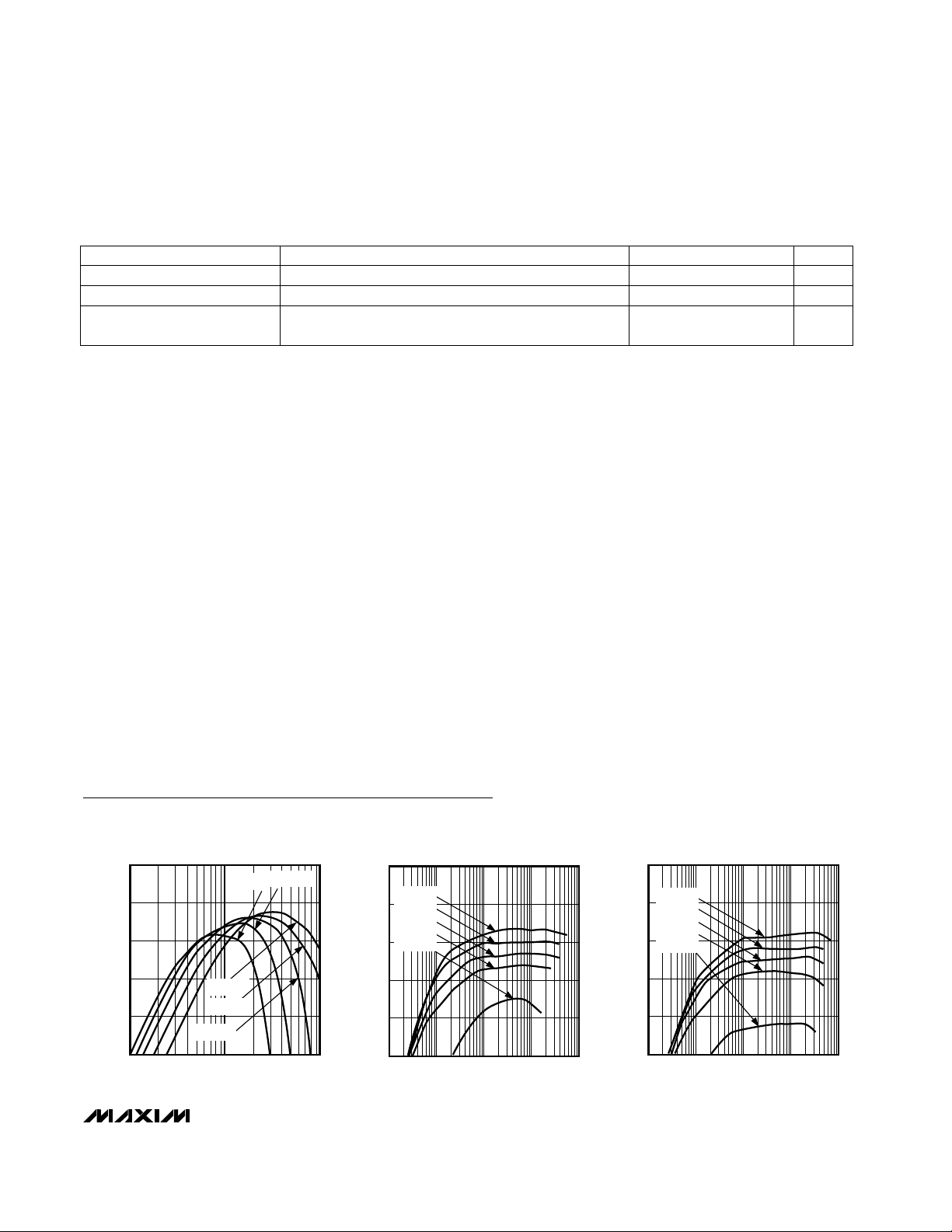
Typical Operating Characteristics
(TA = +25°C, unless otherwise noted.)
100
50
1 10 100
EFFICIENCY vs. LOAD CURRENT
(RUN MODE, V
OUT
= 3.0V)
60
MAX769-01
LOAD CURRENT (mA)
EFFICIENCY (%)
70
80
90
V
IN
= 5.0V
V
IN
= 1.5V
V
IN
= 2.0V
V
IN
= 3.5V
V
IN
= 2.5V
100
50
0.01 1 100.1 100
EFFICIENCY vs. LOAD CURRENT
(COAST MODE, V
OUT
= 3.0V)
60
MAX769-02
LOAD CURRENT (mA)
EFFICIENCY (%)
70
80
90
V
IN
= 5.0V
V
IN
= 3.5V
V
IN
= 2.5V
V
IN
= 2.0V
V
IN
= 1.5V
100
50
0.01 1 100.1 100
EFFICIENCY vs. LOAD CURRENT
(COAST MODE, V
OUT
= 2.4V)
60
MAX769-03
LOAD CURRENT (mA)
EFFICIENCY (%)
70
80
90
V
IN
= 5.0V
V
IN
= 3.5V
V
IN
= 2.5V
V
IN
= 2.0V
V
IN
= 1.5V
Page 6

MAX769
2 or 3-Cell, Step-Up/Down,
Two-Way Pager System IC
6 _______________________________________________________________________________________
Typical Operating Characteristics (continued)
(TA = +25°C, unless otherwise noted.)
100
10
1 4 532 6
NO-LOAD BATTERY CURRENT
vs. BATTERY VOLTAGE
MAX769-04
BATTERY VOLTAGE (V)
BATTERY CURRENT (µA)
V
OUT
= 3.0V
COAST MODE
160
140
120
100
80
60
40
20
0
1 4 532 6
MAXIMUM LOAD CURRENT
vs. BATTERY VOLTAGE
MAX769-05
BATTERY VOLTAGE (V)
MAXIMUM LOAD CURRENT (mA)
RUN MODE
COAST MODE
V
OUT
= 3.0V
6
1
1 10 100
START-UP BATTERY VOLTAGE
vs. LOAD CURRENT
2
MAX769-06
LOAD CURRENT (mA)
START-UP BATTERY VOLTAGE (V)
3
4
5
V
OUT
= 3.0V
COAST MODE
0
5
15
10
20
25
0 21 3 4 5 6
NICD CHARGING CURRENT vs.
NICD VOLTAGE
MAX769-07
NICD VOLTAGE (V)
NICD CHARGING CURRENT (mA)
15mA MODE
V
OUT
= 4.9V
0
2
1
3
0 21 3 4 5
DR1 OR DR2 ON-RESISTANCE vs. V
OUT
MAX769-08
V
OUT
VOLTAGE (V)
R
ON
(Ω)
-80
-60
-40
0
-20
20
100 300200 400 500 600
LX NOISE SPECTRUM
(RUN MODE, SYNC OPERATION)
MAX769-09
FREQUENCY (kHz)
NOISE (dBV)
0
20
60
80
40
100
0.1 101 100 1000 10,000
REG2 NOISE SPECTRUM
(RUN MODE)
MAX769-10
FREQUENCY (kHz)
NOISE (dBµV)
Page 7

MAX769
2 or 3-Cell, Step-Up/Down,
Two-Way Pager System IC
_______________________________________________________________________________________ 7
Pin Description
25 OUT
DC-DC Converter Output and Feedback Point. Digitally controlled from 1.8V to 4.9V in 100mV steps
(Table 5).
27
CS
Chip Select for SPI Serial Interface
28 LX2
Connect LX2 to the other inductor terminal. LX2 is internally connected to an NFET that switches to PGND
and a PFET that switches to BATT.
26 BATT Positive Connection to Battery. The IC is powered from OUT.
24 REG1
PFET Output Connected to OUT. Output is clamped such that it cannot rise above 3.3V, regardless of the
voltage set at OUT.
20 REG3 1V, 2mA Regulator Output. On via the serial interface. Low noise.
22 R2IN REG2 Input. Connect to OUT, REG1, or another voltage source.
23 NICD
15mA or 1mA Settable Charge Current from OUT to 3-Cell NiCd Stack. When the NICD_REG_ON bit is set
(Table 1), NICD becomes an input to the linear regulator at OUT, and the DC-DC converter is off.
21 REG2
24mA REG2 Output. Linearly regulated to the voltage at the OFS pin (voltage difference = 10µA x R
OFS
).
REG2 isolates noise.
18 DR2IN Logic Input. ANDed with the DR2ON bit to control the DR2 switch.
19 DR2 Open-Drain FET Switch. On via AND of the DR2ON bit and the DR2IN pin.
17 DR1 Open-Drain FET Switch. Activated via the serial-interface bit.
9 CH0
CH0 is compared to a 7-bit DAC that adjusts from 0.2V to 1.27V. The comparison result is sent to the CH0
OUT register.
13 SYNC
Sync Input for PWM Switch Rate. A 38.4kHz input results in a 268.8kHz PWM rate (seven times the SYNC
frequency).
15 AGND Analog Ground
16 DRGND Ground for DR1 and DR2 FET Sources
14 OFS Resistor sets offset between OUT (or REG1 or any other point) and REG2. R
OFS
= 15kΩ results in 150mV.
11 LBI Low-Battery Input. Triggers LBO and internal serial bit.
12 FILT
An external RC network sets the PLL loop response to adjust frequency lock time versus jitter: 1nF || (22nF +
10kΩ).
10 RSIN Reset Input. Triggers RSO and resets IC when input is below 0.6V. Comparator with hysteresis (18mV).
5 SCL Serial Clock for SPI Interface
7 RSO
Reset Output. Open drain goes low when RSIN drops below 0.6V. All serial registers are reset (or set) to
POR state as well.
8 REF 1.28V Reference. Bypass with a 1µF capacitor.
6 LBO Open-Drain Output for LBI Comparator
3 SDO Serial Data Output for SPI Interface
4 PGND Power Ground. Source of LX1 and LX2 NFETs.
2 SDI Serial Data Input for SPI Interface
NAME FUNCTION
1 LX1
Connect LX1 to the inductor. LX1 is internally connected to an NFET that switches to PGND and a PFET that
switches to OUT.
PIN
Page 8
MAX769
2 or 3-Cell, Step-Up/Down,
Two-Way Pager System IC
8 _______________________________________________________________________________________
LB0
TO S1
AND S2
LBI
CH0
0.6V
CH0
RUN/
COAST
OV0–OV4
SERIAL
I/O
CH1
CH2
S1
7
DAC0–DAC7
RESET
CONTROL
V FEEDBACK
CHARGE
NICD
OR
BACKUP
REGULATOR
PWM
(PFM IN
COAST)
CHG/REG
+
–
CP
LB
CP0
CP1
CP2
N
6
11
25 27
SDOSDISCL
3 26
9
REF
0.6V
1µF
10µA
1.0V
REG3
1µF
8
5
RSIN
10
17 18 19 16 15
20
21
14
DR1 DR2IN DR2
AGNDDRGND
N
1.8Ω
1.8Ω
REG2 ON
REG3 ON
N N
P
P
7
–
+
+
–
+
–
FROM
NICD
FROM
BATTERY
7-BIT
CH
DAC
S2
5
REG2
REG1
R2IN
C
OFS
0.1µF
OFS
NICD
R
OFS
15k
10µF
10µF
OUT
SYNC
FILT
PGND
LX2
LX1
BATT
P
N
N
P
2- OR 3-CELL
BATTERY IN
L1
68µH
22µF
47µF
+
A
OUT
+
–
CS
1.28V
REFERENCE
1.0V
–
+
BACKUP
REGULATOR
CLAMP ON WHEN
OV4 = 1
3.3V
CLAMP
1mA/15mA
3.3V
P
–
+
–
+
A
R1
A
R2
A
R3
22
23
24
25
13
1nF
22nF
10k
12
28
X7
PLL
LBO
RSO
MAX769
4
1
CP
RS
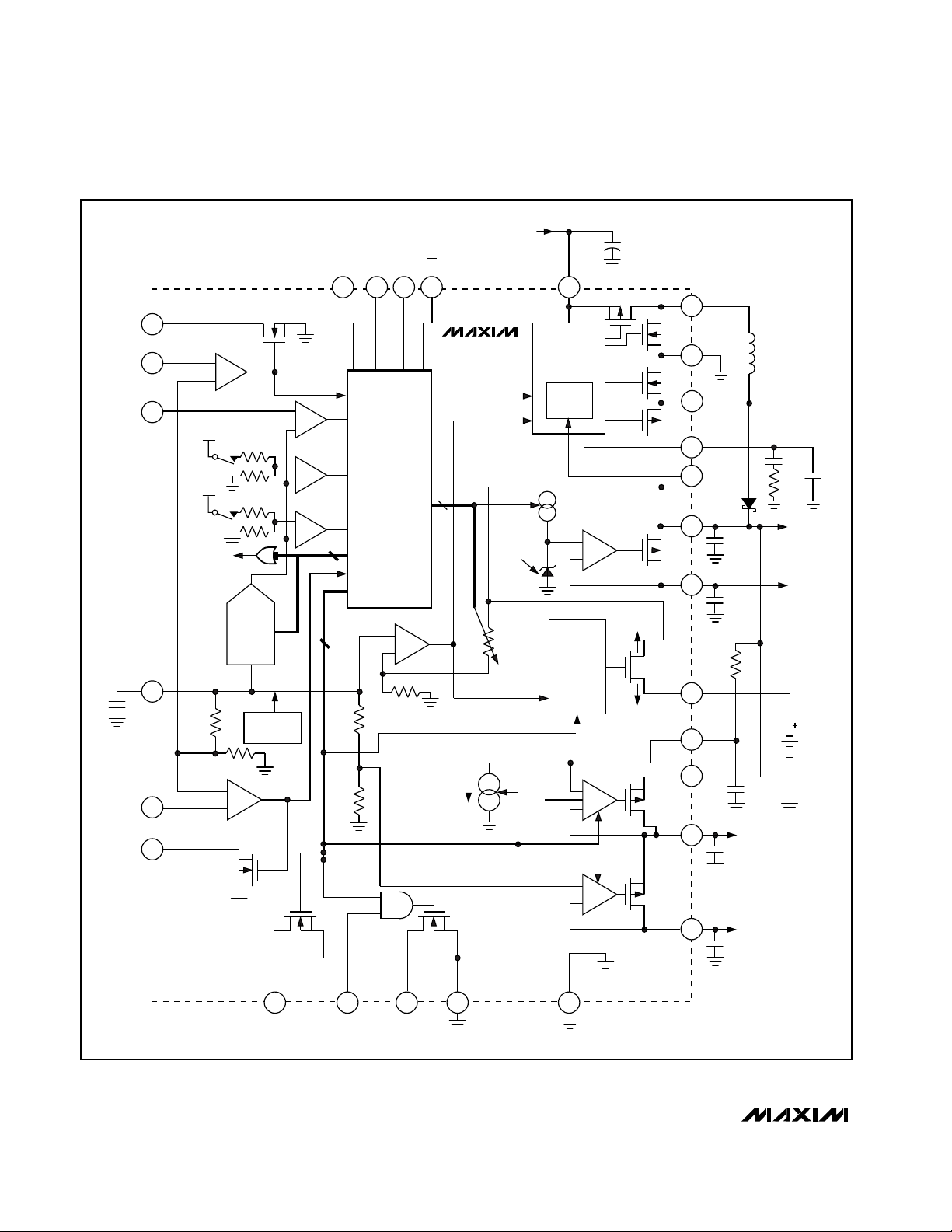
Figure 1. MAX769 Block Diagram
Page 9

MAX769
2 or 3-Cell, Step-Up/Down,
Two-Way Pager System IC
_______________________________________________________________________________________ 9
_______________Detailed Description
The MAX769 contains several functional blocks that
simplify the integration of power-supply and monitoring
functions within a 2 or 3-cell powered system. They are
described in the following subsections.
Voltage Regulators
Regulator outputs include the following:
• OUT: Main switch-mode buck/boost output
• REG1: 1.5Ω switch and output voltage clamp. Switches
REG1 to OUT and clamps REG1 at 3.3V when
OUT is set to 3.4V or more.
• REG2: Linear-regulated, 24mA low-noise output that
regulates so that V
OUT
- V
REG2
is a set difference
voltage (10µA x R
OFS
). Output peak-to-peak ripple is
typically 2mV with a 10µF bypass capacitor at REG2.
REG2 clamps the output at 3.3V when OUT is set to
3.4V or more.
• REG3: Low-noise, 1V linear regulator that supplies
2mA.
Main DC-DC Boost Converter (OUT)
OUT is the main DC-DC converter’s output. It supplies
current from the internal synchronous-rectified buck/
boost regulator and needs no external FETs or voltagesetting resistors. The output voltage (V
OUT
) is adjusted
from 1.8V to 4.9V in 100mV steps (Tables 1 and 5) by
internal DAC control using a serial-data command.
OUT can supply up to 80mA, less the current supplied
to the other regulators (REG1, REG2, and REG3).
OUT can also be put into a low-current, pulse-skipping
Coast Mode (13µA typical quiescent current) by resetting the RUN/COAST serial input bit. OUT supplies up
to 40mA in Coast Mode. Typically, when changing from
Run to Coast Mode, a lower OUT voltage is also set
(Table 4) to further reduce system operating current.
The extent of this reduction depends on the minimum
operating voltage of the system components when they
are in standby or sleep states.
OUT can be set as low as 1.8V; however, some Run
Mode functions are limited when V
OUT
is below 2.5V:
• The allowed serial-interface clock rate is reduced.
• Internal LX FET and DR1 and DR2 on-resistance
increases.
Logic Supply (REG1)
REG1 is not a regulator in the conventional sense, but
rather a 1.5Ω PFET that acts as either a switch or a voltage clamp, depending on the programmed OUT voltage. When OUT is set to 3.3V or less, REG1 operates
as a switch. When OUT is set to 3.4V or more, the
REG1 output clamps at 3.3V. This arrangement limits
V
REG1
to an acceptable voltage for logic when OUT is
programmed to a higher voltage (typically >4V) for
charging (see
Charger Circuit
and
Backup Linear
Regulator
sections).
Low-Noise Analog Supply (REG2)
REG2 is a linear, 24mA low-dropout regulating circuit
whose input is R2IN. The REG2 output (V
REG2
) is set
by R
OFS
. R
OFS
does not set an absolute voltage, but
rather an offset level from R2IN (Figure 2). V
REG2
is set
by:
V
REG2
= V
R2IN
- 10µA x R
OFS
Typically R2IN and R
OFS
are tied to OUT, in which
case:
V
OUT
- V
REG2
= 10µA x R
OFS
ROFS adjusts V
REG1
- V
REG2
to allow REG2 noise
rejection to be traded for voltage drop and consequent
efficiency loss. A 15kΩ (typical) R
OFS
value sets a
150mV voltage difference. R2IN is typically supplied
from OUT or REG1, but can be connected elsewhere
as long as the voltage applied to R2IN does not exceed
V
OUT
. For lowest output noise on REG2, connect R2IN
to REG1.
Note that the REG2 output also clamps at 3.3V when
OUT is set to 3.4V or higher.
Low-Noise, 1V Analog Supply (REG3)
REG3 is a 1V, low-noise linear regulator that supplies
up to 2mA. REG3’s input is internally connected to
REG2.
PWM Frequency Synchronization
The DC-DC converter switching frequency in pulsewidth-modulation (PWM) mode is nominally 270kHz if
no synchronization clock is supplied and FILT is tied to
REF. If the PLL is used, a filter network is connected to
FILT, a clock is applied to SYNC, and the internal oscillator locks to seven times the input clock rate. The
MAX769 is designed for a 38.4kHz SYNC input and
hence a 268.8kHz operating frequency. PWM switching
frequency is unaffected by the serial-data clock rate.
Voltage Detectors (LBO and Reset)
The MAX769 contains two voltage-detector inputs: LBI
and RSIN. The LBI and RSIN comparator outputs are
open-drain pins (LBO and RSO) for a real-time hardware output. LBO is also readable via the serial interface. Both LBI and RSIN trigger at a 0.6V input
threshold and have about 18mV hysteresis. RSO also
triggers the MAX769 internal power-on reset (POR).
Page 10

MAX769
2 or 3-Cell, Step-Up/Down,
Two-Way Pager System IC
10 ______________________________________________________________________________________
7-Bit ADC (CH0 Input and CH1, CH2)
Three analog channels are compared to a 7-bit, serially
programmed digital-to-analog converter (CH DAC). The
CH DAC voltage can be varied in 10mV steps from
200mV to V
REF
- 1LSB (or 1.27V) (Table 1). CH0 is an
external input, while CH1 and CH2 are signals internally
generated from the NICD and BATT pins. NICD and
BATT are internally divided by four before being compared to CH DAC. The comparison threshold voltages
for each channel are described in the following equations:
V
TH
(CH0: pin 9) = D x 10mV
VTH(CH1: NICD) = D x 40mV
V
TH
(CH2: BATT) = D x 40mV
where D is the decimal equivalent of the binary code
DAC0–DAC6 (Table 1). DAC0 is the LSB. A DAC code
of 1111111 equates to D = 127. When all zeros are programmed, the CH DAC and CH_ comparators turn off.
CH0, CH1, and CH2 comparison results reside in the
three MSB locations of the output serial data (Table 4).
The CH_ OUT data is delayed by one read cycle. In
other words, each CH_ OUT bit is the result of the comparison made against the CH DAC voltage programmed
during the previous serial-write operation.
An analog-to-digital (A/D) conversion can be performed
on a channel by using the system software to step
through a successive-approximation routine or, if the
input is partially known, by setting the CH DAC to a
voltage near the estimated point and checking successive CH_ OUT bits.
MAX769
2 OR 3-CELL
AA ALKALINE
BATTERY
BATT
26
1
11
6
9
27
5
2
3
28
25
4
24
22
14
21
20
10
7
23
15
C
OFS
0.1µF
3.0V
LOGIC
2.85V
ANALOG
1V RCVR
R4
470k
R3
1.3M
100k
3-CELL
NiCd
TO RF
PA
R
OFS
, 15k
LX2
OUT
PGND
REG1
R2IN
OFS
REG2
L1
68µH
D1
MBR0520L
C6
0.1µF
C1
47µF
C2
10µF
C3
10µF
TO µC
RESET
C4
1µF
C5
22µF
SERIAL
I/O
A/D IN
R5
270k
17
19
18
16
13
12
8
1.8Ω
DRIVERS
38.4kHz
C10
22nF
C8
1µF
C9
1nF
REG3
RSIN
RSO
NICD
AGND
LBI
R1
1M
R2
250k
REG1
LBO
CH0
CS
SCL
SDI
SDO
DR1
DR2
DR2IN
DRGND
SYNC
FILT
REF
LX1
10k
Figure 2. Standard Application Circuit
Page 11

MAX769
2 or 3-Cell, Step-Up/Down,
Two-Way Pager System IC
______________________________________________________________________________________ 11
A faster A/D shortcut can be used for battery measurements when the goal is a “go, no go” determination. For
this type of test, the CH DAC can simply be set to the
desired limit, and CH_ OUT supplies the result on the
next serial-write operation. One instance in which this
shortcut saves time is during a battery-impedance
check. The unloaded battery voltage can first be measured, if time allows, using one of the techniques
described in the previous paragraph. Then the magnitude of the loaded voltage drop can be quickly
checked with a single comparison to see if it is within
the desired limit.
The A/D circuitry can be invoked in both Run and Coast
Modes.
Open-Drain Drivers
Two open-drain drivers (DR1 and DR2) are activated
via the serial interface. DR1 and DR2 are grounded
1.8Ω (typical) NFETs that can sink up to 120mA. The
maximum sink current is limited by on-resistance and
package dissipation to about 240mA total sink current
for both switches. Note that DR1 and DR2 are designed
to sink current only from the main battery (BATT) and
cannot be pulled above BATT.
DR2 is controlled by an external input (DR2IN) as well as
a serial input bit. DR2IN is ANDed with the DR2ON serialcontrol bit, allowing DR2 to drive an audio beeper. The
audio-frequency clock is applied to DR2IN, and ON/OFF
gating is applied to DR2ON. Both DR2IN (pin 18) and
DR2ON (serial bit) must be high for DR2 to switch on.
Coast Mode/Voltage Selection
Reduce the operating current by setting the RUN/COAST
bit low via the serial input. This shifts the DC-DC boost
converter from low-noise PWM operation (Run Mode) to
a very low operating current mode (Coast Mode) in
which switching pulses are only provided as needed to
satisfy the load. To further reduce operating current in
Coast Mode, lower V
OUT
using the OV0–OV4 serial bits.
The MAX769 starts up in Coast Mode. Select Run Mode
with the serial interface after power-up.
Various circuit functions can be disabled as follows:
Functions that
always remain on in Coast Mode are:
• Serial I/O
• Reference (REF)
• OUT
• REG1
• LBI, RSIN (and LBO, RSO)
Functions that can be
programmed on or off in Coast
Mode
are (Table 1):
• DR1 and DR2
• REG2 and REG3
• NICD charger (Note: This may overload OUT if
turned on in Coast Mode when other loads are present)
• Backup regulator
• CH0, CH1, CH2, and CH DAC
Functions that
always turn off in Coast Mode
are:
• SYNC and PLL circuits
• DC-DC PWM control circuits
Power-On Reset
The MAX769 has an internal POR circuit (V
OUT
< 1.6V)
to ensure an orderly power-up when a battery is first
applied. This feature is separate from the RSO comparator; however, if RSO goes low during operation, all
serial registers are set to the same predetermined
states as on power-up. The POR states for each register are listed in Table 2.
Note that the MAX769 always comes out of reset in
Coast Mode; consequently, it cannot supply full power
until Run Mode is selected by serial command. System
software cannot exercise full load current until Run
Mode is enabled.
Charger Circuit
A charger current source from OUT to NICD is activated via a serial bit (Table 1). The current source can
charge a small 3-cell NiCd or NiMH battery (typically a
coin cell) or a 1-cell lithium battery. The charge current
can be set to either 15mA or 1mA. OUT sets the maximum charge (or float) voltage. When charging is implemented, V
OUT
must also be set high enough to allow
sufficient headroom for the charger current source. The
V
OUT
- V
NICD
difference should normally be between
0.2V and 0.5V. Charger current vs. NICD voltage is
graphed in the
Typical Operating Characteristics
. Note
also that charging current reduces the OUT current
available for other loads.
Backup Linear Regulator
The BACKUP serial input bit turns on the backup regulator, which sources current from NICD to OUT. This
regulator backs up OUT by using the rechargeable battery (at NICD) when the main battery (at BATT) is
depleted or removed. The backup regulator pass
device’s resistance is typically 5Ω, so it can typically
supply 20mA with only 100mV of dropout.
Page 12

MAX769
2 or 3-Cell, Step-Up/Down,
Two-Way Pager System IC
12 ______________________________________________________________________________________
Table 1. Serial-Bit Assignments
Table 2. Serial-Bit Power-On Reset (POR) States
Table 3. Input-Bit Function Description
Table 4. Serial Output Data
R2 (MSB) R0 D3 D1
0 0 DR1_ON REG2_ON
0 1
LBO_Sets_
BACKUP
15mA_CHG
0 0 OV3 OV1
0 1 X X
R1
0
0
1
1
D4
DR2_ON
X
OV4
X
D2 D0
RUN/
COAST
1mA_CHG
OV0
X
REG3_ON
BACKUP
OV2
X
1 DAC5 DAC3 DAC1DAC6 DAC4 DAC0DAC2
R2 R0 D3 D1
0 0 POR = 0 POR = 0
0 1 POR = 0 POR = 0
0 0
POR = 1
POR = 0
0 1 X X
R1
0
0
1
1
D4
POR = 0
X
POR = 0
X
D2 D0
POR = 0
POR = 0
POR = 0
X
POR = 0
POR = 0
POR = 1
X
1 POR = 0 POR = 0 POR = 0POR = 0 POR = 0 POR = 0POR = 0
Sets 7-bit CH DAC voltage for A/D conversion (POR state is all zeros with DAC and comparators off).DAC0–DAC6
Sets OUT Output Voltage (POR state is V
OUT
= 3.0V).OV0–OV4
1 = Allows LBO to turn on the backup regulator and disable the DC-DC converter (POR state is no
connection between LBO and BACKUP).
LBO_Sets_BACKUP
1 = Turns on the backup linear regulator from NICD to OUT and disables the DC-DC converter (POR
state is BACKUP off). Setting this bit overrides 1mA_CHG, 15mA_CHG, and LBO_Sets_BACKUP
(Figure 1).
BACKUP
1 = Turns on the selected charge current to NICD. If both are set, the charge current is 15mA (POR
state is off).
1 = Turns on the selected switch (POR state is off).
1 = Turns on the selected regulator (POR state is off).
1 = Run Mode, 0 = Coast Mode (POR state is Coast Mode).
FUNCTION
1mA_CHG, 15mA_CHG
DR1, DR2
REG2_ON, REG3_ON
RUN/COAST
INPUT BIT
D7 (MSB) D5 D3–D0
CH2_OUT CH0_OUT X
D6
CH1_OUT
D4
LBO
FUNCTION
CH_OUT and LBO output bits. A 1 indicates
that the selected channel (CH_) voltage is
greater than the CH DAC voltage or that LBI is
less than 0.6V.
Page 13

MAX769
2 or 3-Cell, Step-Up/Down,
Two-Way Pager System IC
______________________________________________________________________________________ 13
All DC-DC converter and charging circuitry is disabled
when the backup regulator is turned on, but all other
functions remain active. Activate BACKUP manually or by
serial command, or set it to trigger automatically via LBO.
Automatic Backup
Setting the LBO_Sets_BACKUP serial bit (Table 1) programs the IC so that when LBO goes low, the backup
regulator automatically turns on without instructions from
the microprocessor (µP). When the LBO_Sets_BACKUP
bit is 0, the backup regulator is turned on only by setting
the BACKUP bit. The BACKUP bit also overrides the
LBO_Sets_BACKUP bit. Figure 3 shows the logic for this
function.
If the main battery is depleted and the NiCd battery is
drained during backup, RSO goes low while the backup regulator is supplying OUT (if RSI is used to monitor
OUT or REG1). When RSO falls, the serial registers
reset to their POR states (with the DC-DC converter on
in Coast Mode and the backup regulator off, see
Tables 1, 2, and 3). This prevents the IC from getting
hung up with the DC-DC converter off when a new main
battery is inserted. This sequence is required because
if the MAX769 did not default to “DC-DC converter on”
when coming out of reset, the µP (still reset by RSO)
would not be able to provide the device with serial
instructions to turn on.
Serial Interface
The MAX769 has an SPI-compatible serial interface.
The serial-interface lines are Chip Select (CS), Serial
Clock (SCL), Serial Data In (SDI), and Serial Data Out
(SDO). Serial input data is arranged in 8-bit bytes. Most
bytes contain a 3-bit address pointer (R2, R1, R0)
along with 5 bits of input data (D4–D0). For common
operations such as selecting Run or Coast Mode, activating REG2 or REG3, or turning on DR1 or DR2, only
the 000 (R2, R1, R0) address register needs to be written. The serial input data format for all MAX769 operations is outlined in Tables 1, 2, and 3.
15mA_CHG
1mA_CHG
TO
CHARGER
CONTROL
TO
BACKUP
REGULATOR
BACKUP
LBO_SETS_BACKUP
LBO
Figure 3. Logic for Charger Control and BACKUP and for
LBO_Sets_BACKUP Serial Input Bits
2.510 110
4.911 111
4.811 011
4.701 111
4.601 011
4.511 101
4.411 001
4.301 101
4.201 001
4.110 111
4.010 011
3.900 111
3.800 011
3.710 101
3.610 001
3.500 101
3.400 001
3.311 110
3.211 010
3.101 110
3.001 010
2.911 100
2.811 000
2.701 100
2.601 000
2.410 0
1.9
1.8
10
V
OUT
(V)
2.300
0
0
OV1
110
2.20
0
0
OV3
0 010
2.110 100
2.0
100
000
OV0OV2OV4
10 000
Table 5. V
OUT
Output Voltage
SERIAL-DATA BIT
Page 14

MAX769
2 or 3-Cell, Step-Up/Down,
Two-Way Pager System IC
14 ______________________________________________________________________________________
Serial data is clocked in and out MSB first. Input data is
latched on the CLK rising edge, and output data is
shifted out on the CLK falling edge. When CS goes low,
DO immediately contains the MSB output bit (D7). D6 is
not clocked out until the falling clock edge that follows
the first rising clock edge after a Chip Select. See the
timing diagrams in Figures 4 and 5.
SPI writes and reads concurrently, so it may be necessary to perform dummy writes in order to read output
data. Four output data bits (D7–D4, Table 4) are sent
from SDO each time a serial operation occurs.
When R2 = 0, R0 and R1 are address pointers.
However, when R2 = 1, the 7 remaining bits (R1, R0
and D4–D0) become DAC programming bits. This violation of programming etiquette (R1 and R0 are sometimes address bits and other times data bits) allows the
CH DAC to be loaded with only one write operation.
Writing all zeros to the CH DAC turns it, the CH0, CH1,
and CH2 comparators, and the NICD and BATT voltage-sensing resistors off to minimize current consumption. This reduces current drain from OUT by about
30µA.
• • •
• • •
• • •
• • •
CS
SCLK
DIN
DOUT
t
CSH
t
CSS
t
CL
t
DS
t
DH
t
DV
t
CH
t
DO
t
TR
t
CSH
Figure 4. Detailed Serial-Interface Timing
CS
SCL
SCO D7 D6
R1R2 D4R0 D2D3 D0D1
D5 D4 0 0 0 0
SDI
Figure 5. CS, SCL, SDO, and SDI Serial Timing
Page 15
MAX769
2 or 3-Cell, Step-Up/Down,
Two-Way Pager System IC
______________________________________________________________________________________ 15
Applications Information
Component Selection
The MAX769 requires minimal design calculation and is
optimized for the component values shown in Figure 2.
However, some flexibility in component selection is still
allowed, as described in the following text. A list of suitable components is provided in Table 6.
Inductor L1 is nominally 68µH, but values from 47µH to
100µH should be satisfactory. The inductor current rating should be 300mA or more if full output current
(80mA) is needed. If less output current is required, the
inductor current rating can be reduced proportionally
but should never be less than 150mA.
Inductor resistance should be minimized for best efficiency, but since the MAX769 N-channel switch resistance is typically 0.9Ω, efficiency does not improve
significantly for coil resistances below 0.4Ω.
Filter capacitors C1–C4 should be low-ESR types (tantalum or ceramic) for lowest ripple and best noise
rejection. The values shown in Figure 2 are optimized
for each output’s rated current. Lower required output
current allows smaller capacitance values.
Resistors at the LBI and RSIN inputs set the voltage at
which the LBO and RSO outputs trigger. The voltage
threshold for both LBI and RSI is 0.6V. The resistors
required to set a desired trip voltage, (Figure 2) V
TRIP
,
are calculated by:
R1 = R2[(V
TRIP(LBO)
/ 0.6) - 1]
R3 = R4[(V
TRIP(LBO)
/ 0.6) - 1]
To minimize battery drain, use large values for R2 and
R4 (>100kΩ) in the above equations; 470kΩ is a good
starting value.
See the
Low-Noise Analog Supply (REG2)
section for
information on selecting R
OFS
.
Since LBO and RSO are open-drain outputs, pull-up
resistors are usually required. Normally these will be
pulled up to REG1. 100kΩ is recommended as a compromise between response time and current drain,
although other values can be used. Since LBI and RSO
are high (open circuit) during normal operation, current
normally does not flow in the pull-up resistors until a
low-battery or reset event occurs.
Logic Levels
Note that since the MAX769’s internal logic is powered
from REG1, the input logic levels at the digital inputs
(DR2IN, RUN, SYNC, CS, and SDI) as well as the logic
output level of SDO are governed by the voltage at
REG1. Logic-high inputs at these pins should not
exceed V
REG1
. Digital inputs should either be driven
from external logic (or a µP) powered from REG1, or by
open-drain logic devices that are pulled up to REG1.
Board Layout and Noise Reduction
The MAX769 makes every effort in its internal design to
minimize noise and EMI. Nevertheless, prudent layout
practices are still suggested for best performance.
Recommendations are as follows:
1) Keep trace lengths at L1, LX1, and LX2, as well as
at PGND, as short and wide as possible. Since LX1
and LX2 toggle between V
BATT
and V
OUT
at a fast
rate, minimizing the trace length serves to reduce
excess PC board area that might act as an antenna.
2) Place the filter capacitors at OUT, REG1, REG2,
and REG3 as close to their respective pins as possible (no more than 0.5mm away).
3) Consider using an inductor at L1. A shielded inductor at L1 will minimize radiated noise, but may not
be essential. Toroids will also exhibit EMI performance similar to that of shielded coils.
4) Keep the power components at the uppermost part
of the IC to minimize coupling to other parts of the
circuit. The LX1, LX2, OUT, and PGND pins are
located at the uppermost part of the IC to facilitate
PC board layout. Other pins in this area are digital
and are not affected by close proximity to switching
nodes.
5) Use a separate short, wide ground trace for PGND
and the ground side of the BATT and OUT filter
capacitors. Tie this trace to the ground plane.
Table 6. External Components
SUPPLIER PART NO. COMMENTS
CD54-680
LQH4N680K
1.9Ω, 2.6mm high,
low current, low cost
Murata
Sumida
0.46Ω, 4.5mm high
CDR74B-680
Coilcraft
DT1608C-223,
DT1608C-683
0.58Ω, 3.18mm high,
shielded
AVX TPS series Tantalum
Marcon THCR series Ceramic
Sprague 595D series Tantalum
TDK C3216 series Ceramic
0.33Ω, 4.5mm high,
shielded
CD73-680
0.33Ω, 3.5mm high
Polystor A-10300 1.5 Farads
INDUCTORS (68µH)
CAPACITORS
STORAGE CAPACITOR (optional at NICD pin)
Page 16

MAX769
2 or 3-Cell, Step-Up/Down,
Two-Way Pager System IC
16 ______________________________________________________________________________________
Pin Configuration
________________________________________________________Package Information
28
27
26
25
24
23
22
21
20
19
18
17
16
15
1
2
3
4
5
6
7
8
9
10
11
12
13
14
LX2
CS
BATT
OUT
REG1
NICD
AGND
R2IN
REG2
REG3
DR2
DR2IN
DR1
DRGND
OFS
SYNC
FILT
LBI
RSIN
CH0
REF
RSO
LBO
SCL
PGND
SDO
SDI
LX1
QSOP
TOP VIEW
MAX769
QSOP.EPS
 Loading...