

Page 1
19-1174; Rev 0; 12/96
Low-Noise, Dual-Output, Regulated Charge Pump
for GaAsFET, LCD, and VCO Supplies
_______________General Description
The MAX768 low-noise, dual-output, regulated charge
pump provides a negative output for biasing GaAsFET
power amplifiers, and a positive output for powering
voltage-controlled oscillators (VCOs) in wireless handsets. The outputs can also be used to power LCDs.
Output ripple is less than 2mVp-p. The MAX768 is
intended for use in low-voltage systems where a simple
charge-pump inverter is inadequate, or where the VCO
needs more range to improve its signal-to-noise ratio.
The input range is 2.5V to 5.5V, enabling direct power
from 1Li+ and 3-cell NiMH/NiCd batteries.
The MAX768 includes a voltage-doubler charge pump,
followed by an inverting charge pump. This combination produces unregulated outputs that are ±2x the
input. Two internal low-dropout linear regulators provide
the low-noise, regulated positive and negative outputs.
Output current is guaranteed to be at least 5mA per
output. The linear regulators use CMOS devices, so the
quiescent current remains independent of output loading (even in dropout), and the dropout voltage
approaches zero with no load current.
The MAX768 has two preset switching frequencies
(25kHz or 100kHz), or can be synchronized by an external clock from 20kHz to 240kHz. This flexibility permits
users to optimize their designs based on noise, capacitor size, and quiescent-supply-current criteria.
The device features Dual Mode™ operation: the output
voltage is preset to +5V and -5V, or can be adjusted by
adding external resistor dividers. Other features include
independent shutdowns and a logic output that signals
when the negative voltage has risen to within 10% of its
regulation setpoint (to protect the power amplifier
GaAsFET). The MAX768 is available in a space-saving,
16-pin QSOP, which is the same size as a standard
8-pin SO.
________________________Applications
GaAsFET Power Amp Bias
Voltage-Controlled Oscillator (VCO) Supply
Tuner Diode Power Supply
Positive and Negative LCD Supply
Cellular Phone
PCS and Cordless Phone
Wireless Handsets
Wireless Handheld Computers
Wireless PCMCIA Cards
Modems
____________________________Features
♦ Dual Positive/Negative Regulated Outputs:
±5V
♦ Output-Ready Indicator to Protect GaAsFET PAs
♦ 2.5V to 5.5V Input Voltage Range
♦ Low-Noise Output Ripple: < 2mVp-p
♦ Synchronizable Switching Frequency
♦ Uses Only Small, Low-Cost Capacitors
♦ 0.1µA Independent Shutdown Controls
♦ Adjustable Output Voltages
♦ Small 16-Pin QSOP Package
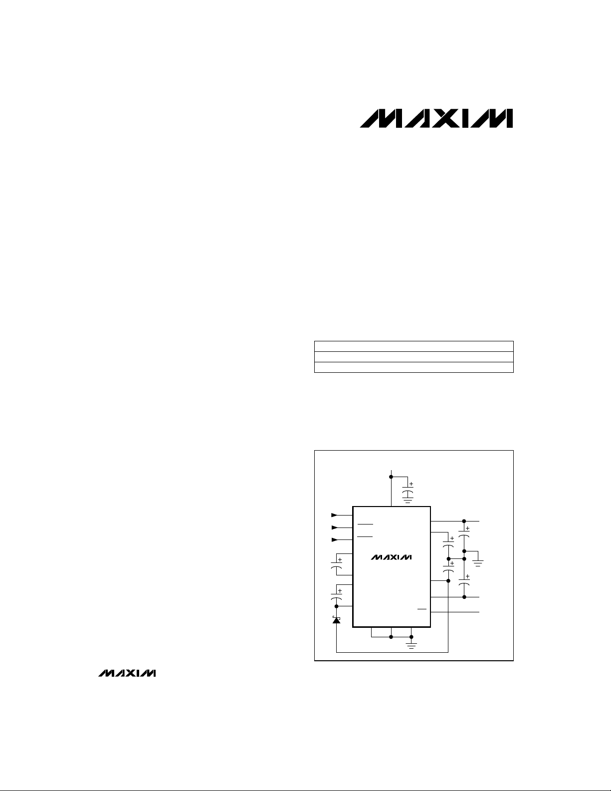
OUT
from 3V
IN
______________Ordering Information
PART
MAX768C/D
MAX768EEE -40°C to +85°C
*
Dice are specified at TA= +25°C, DC parameters only.
Pin Configuration appears at end of data sheet.
Dual Mode is a trademark of Maxim Integrated Products.
TEMP. RANGE PIN-PACKAGE
0°C to +70°C
Dice*
16 QSOP
__________Typical Operating Circuit
VIN
(3.0V TO 5.5V)
C7
C5
C6
POSITIVE
OUTPUT
+5V
NEGATIVE
OUTPUT
-5V
OUTPUT-
READY
SIGNAL
SYNC
PSHDN
NSHDN
C1+
C1
C2
C1C2+
C2-
IN
MAX768
GND
POUT
V+
C3
C4
V-
NOUT
RDY
SETPSETN
MAX768
________________________________________________________________
Maxim Integrated Products
1
For free samples & the latest literature: http://www.maxim-ic.com, or phone 1-800-998-8800
Page 2
Low-Noise, Dual-Output, Regulated Charge Pump
for GaAsFET, LCD, and VCO Supplies
ABSOLUTE MAXIMUM RATINGS
VIN, C1-, SYNC, PSHDN, NSHDN to GND...............-0.3V to +6V
V+, C1+, C2+, RDY to GND...................................-0.3V to +12V
SETP to GND .......................................................... -0.3V to +3V
SETN to GND............................................................-3V to +0.3V
V-, C2- to GND ...................................................... -12V to +0.3V
OUTP, OUTN Short Circuited to GND .......................Continuous
NOUT to V- ........................................................... -0.3V to +12V
MAX768
POUT to V+ ........................................................... -12V to +0.3V
Stresses beyond those listed under “Absolute Maximum Ratings” may cause permanent damage to the device. These are stress ratings only, and functional
operation of the device at these or any other conditions beyond those indicated in the operational sections of the specifications is not implied. Exposure to
absolute maximum rating conditions for extended periods may affect device reliability.
Continuous Power Dissipation (T
QSOP (derate 8.70mW/°C above +70°C)......................696mW
Operating Temperature Range
MAX768EEE.......................................................-40°C to +85°C
Maximum Junction Temperature .....................................+150°C
Storage Temperature Range.............................-65°C to +165°C
Lead Temperature (soldering, 10sec).............................+300°C
ELECTRICAL CHARACTERISTICS
(VIN= +3V, SYNC = IN, SETN = SETP = GND, NSHDN = PSHDN = IN, TA= -40°C to +85°C, unless otherwise noted. Typical values
= +25°C. See Figure 2.) (Note 1)
are at T
A
CONDITIONS
I
Minimum Input Start-Up Voltage
No-Load Supply Current at 100kHz
(both regulators active)
No-Load Supply Current at 100kHz
(negative regulator off)
No-Load Supply Current at 25kHz
(both regulators active)
Dropout Voltage (2 x VIN- |V
Output Voltage Noise
SHUTDOWN
SHDN Input Bias Current
OUT
)
|
= 0
LOAD
0mA < I
0mA < I
(Note 2)
(Note 3)
VIN= 3V, V
VIN= 3.0V
VIN= 5.5V 1.5
NSHDN = GND
V
SYNC
2 x VIN- | V
VIN= 3V to 5.5V
I
POUT
I
NOUT
C
POUT =CNOUT
10kHz < f < 1MHz
V
SHDN
NSHDN = PSHDN = SYNC = GND
< 5mA, VIN= 3.0V to 5.5V V4.81 5.00 5.14Positive Output Voltage
LOAD
< 5mA, VIN= 3.0V to 5.5V
LOAD
≥ 4.81V, V
POUT
= GND mA0.45 0.80
I
POUT
OUT
|
I
POUT
= 0mA to 5mA,
= 0mA to -5mA
=
10µF,
= 3V
NOUT
= I
= I
NOUT
NOUT
POUT
NOUT
≤ -4.82V
= 0.1mA
= 5mA
= +70°C)
A
0.8 1.4
20
420 900
1.2
1.7
UNITSMIN TYP MAXPARAMETER
%/mA0.06 0.12Load Regulation
mVp-p
V3.0 5.5Input Voltage Range
V2.5
V-5.10 -5.00 -4.82Negative Output Voltage
V1.25 11Positive Output Voltage Adjustable Range
V-11 -1.25Negative Output Voltage Adjustable Range
mA5Maximum POUT, NOUT Output Currents
mA
mA0.3
mV
%/V-0.12 0.0 0.12Line Regulation
V0.4Shutdown/SYNC Logic-Low Input Threshold
V2.0Shutdown/SYNC Logic-High Input Threshold
µA0.1 2
µA0.1 10Shutdown Supply Current
2 _______________________________________________________________________________________
Page 3
Low-Noise, Dual-Output, Regulated Charge Pump
RDY
for GaAsFET, LCD, and VCO Supplies
ELECTRICAL CHARACTERISTICS (continued)
(VIN= +3V, SYNC = IN, SETN = SETP = GND, NSHDN = PSHDN = IN, TA= -40°C to +85°C, unless otherwise noted. Typical values
= +25°C. See Figure 2.) (Note 1)
are at T
A
CONDITIONS
SYNC
Oscillator Frequency (internal)
SYNC = GND (divide by 4)
V
= 3V
SYNC
SET INPUT
Positive Set-Reference Voltage
Negative Set-Reference Voltage
I
POUT
I
NOUT
V
SETP
= 0.1mA
= 0.1mA
= V
SETN
TA= +25°C
TA= -40°C to + 85°C
TA= +25°C
TA= -40°C to + 85°C
= 1.3V
OUTPUT
RDY Output Threshold
Percent of V
I
= 2mA V0.25Output Low Voltage
SINK
V
= 10V
RDY
NOUT
, I
NOUT
= 5mA
Note 1: Parameters to -40°C are guaranteed by design, not production tested.
Note 2: Maximum output voltage range is from the positive reference voltage to 2 x V
Note 3: Maximum output voltage range is from the negative reference voltage to -2 x V
21.5 25 28.5
85 100 115
1.217 1.25 1.283
1.215 1.25 1.285
-1.270 -1.25 -1.230
-1.275 -1.25 -1.225
- dropout voltage.
IN
+ dropout voltage.
IN
UNITSMIN TYP MAXPARAMETER
MAX768
kHz20 240SYNC Frequency Range (external)
%40 60SYNC Duty Cycle (external)
kHz
µA0.1 2SYNC Input Leakage Current
V
V
µA0.01 0.1SETP, SETN Input Leakage Current
%85 94 98
µA0.01 2Output Off Current
mA10Maximum Sink Current
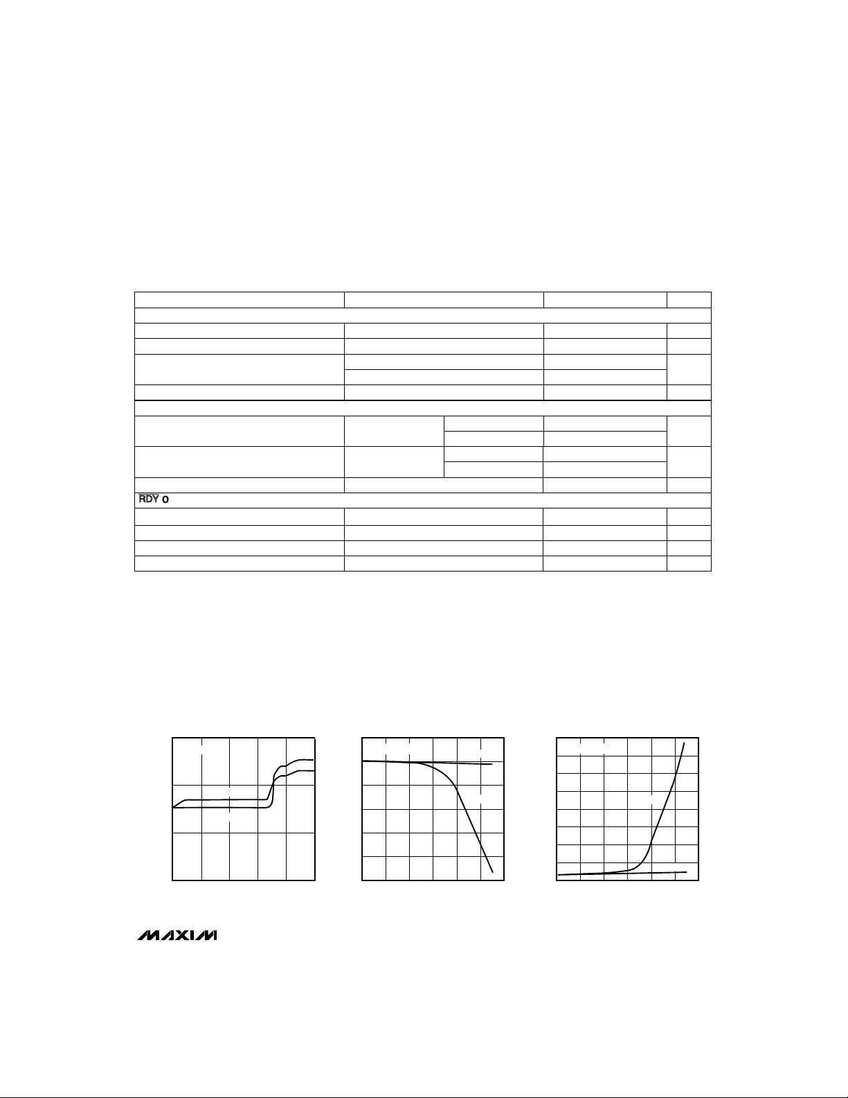
__________________________________________Typical Operating Characteristics
(SYNC = IN, TA = +25°C, unless otherwise noted.)
mV
OUTPUT VOLTAGE
RMS
0.30
)
RMS
0.20
0.10
OUTPUT VOLTAGE (mV
0
vs. OUTPUT CURRENT
IN = 3.0V
NOUT = -5V
POUT = +5V
0 5 15 25
10 20
OUTPUT CURRENT (mA)
_______________________________________________________________________________________ 3
5.2
MAX768-TOC01
5.0
4.8
4.6
4.4
OUTPUT VOLTAGE (V)
4.2
4.0
POUT OUTPUT VOLTAGE
vs. OUTPUT CURRENT
ONLY POUT LOADED
0 5 15 30
10 20 25
OUTPUT CURRENT (mA)
IN = 4.0V
IN = 3.0V
-4.2
-4.3
MAX768-TOC02
-4.4
-4.5
-4.6
-4.7
OUTPUT VOLTAGE (V)
-4.8
-4.9
-5.0
NOUT OUTPUT VOLTAGE vs.
OUTPUT CURRENT
ONLY NOUT LOADED
0 5 15 30
OUTPUT CURRENT (mA)
IN = 3.0V
IN = 4.0V
10 20 25
MAX768-TOC03
Page 4
Low-Noise, Dual-Output, Regulated Charge Pump
for GaAsFET, LCD, and VCO Supplies
____________________________Typical Operating Characteristics (continued)
(SYNC = IN, TA = +25°C, unless otherwise noted.)
4
MAX768
3
2
SUPPLY CURRENT (mA)
1
0
0 40 120 320
SHDN SUPPLY CURRENT
20
vs. SYNC FREQUENCY
18
16
14
12
10
SHDN SUPPLY CURRENT (µA)
90
80
70
60
50
40
EFFICIENCY (%)
30
20
10
0
V
IN
8
6
4
2
0
-40 -15 35 85
EFFICIENCY vs. LOAD CURRENT
(NOUT ONLY LOADED)
V
IN
0.1 1 10 100
LOAD CURRENT (mA)
SUPPLY CURRENT
VIN = 5.0V
V
= 3.3V
IN
16080 200 240 280
SYNC FREQUENCY (kHz)
vs. TEMPERATURE
= 5.0V
V
= 3.3V
IN
TEMPERATURE (°C)
= 3.0V
V
= 4.0V
IN
CHARGE-PUMP FREQUENCY
115
100
MAX768-TOC04
85
70
55
40
CHARGE-PUMP FREQUENCY (kHz)
25
10
0.40
0.35
MAX768-TOC07
0.30
0.25
0.20
0.15
0.10
SHDN SUPPLY CURRENT (µA)
0.05
0
MAX768 TOC10
EFFICIENCY (%)
-0.05
90
80
70
60
50
40
30
20
10
0
6010
vs. SUPPLY VOLTAGE
SYNC = IN
SYNC = GND
2.5 3.0 4.0 6.0
SHDN SUPPLY CURRENT
-40 -15 35 85
EFFICIENCY vs. OUTPUT CURRENT
(POUT ONLY LOADED)
V
IN
0.1 1 10 100
OUTPUT CURRENT (mA)
4.53.5 5.0 5.5
SUPPLY VOLTAGE (V)
vs. TEMPERATURE
V
IN
TEMPERATURE (°C)
= 3.0V
V
= 4.0V
IN
= 5.0V
V
IN
V
IN
= 4.0V
= 3.3V
6010
120
MAX768-TOC05
100
CHARGE-PUMP FREQUENCY (kHz)
MAX768-TOC08
SUPPLY CURRENT (mA)
MAX768 TOC11
EFFICIENCY (%)
CHARGE-PUMP FREQUENCY
vs. TEMPERATURE
V
= 3.3V
IN
SYNC = IN
80
60
40
20
0
-55 -35 5 125
1.8
1.6
1.4
1.2
1.0
0.8
0.6
0.4
0.2
0
2.5 3.0 4.0 6.0
90
80
70
60
50
40
30
20
10
0
0.1 1 10 100
SYNC = GND
25-15 45 8565 105
TEMPERATURE (°C)
SUPPLY CURRENT
vs. SUPPLY VOLTAGE (NO LOAD)
f = 100kHz
f = 25kHz
SUPPLY VOLTAGE (V)
EFFICIENCY vs. OUTPUT CURRENT
LOAD BETWEEN POUT AND NOUT
V
= 3.0V
IN
OUTPUT CURRENT (mA)
5.04.5 5.53.5
V
= 4.0V
IN
MAX768-TOC06
MAX768-TOC09
MAX768 TOC12
4 _______________________________________________________________________________________
Page 5

Low-Noise, Dual-Output, Regulated Charge Pump
for GaAsFET, LCD, and VCO Supplies
_____________________________Typical Operating Characteristics (continued)
(SYNC = IN, TA = +25°C, unless otherwise noted.)
POUT MAXIMUM OUTPUT CURRENT
140
120
100
80
60
40
MAXIMUM OUTPUT CURRENT (mA)
20
0
vs. SUPPLY VOLTAGE
ONLY POUT LOADED
2.5 3.0 4.0
SUPPLY VOLTAGE (V)
MAX768-TOC13
5.04.53.5
TIME TO EXIT SHUTDOWN
NOUT MAXIMUM OUTPUT CURRENT
vs. SUPPLY VOLTAGE
90
ONLY NOUT LOADED
80
70
60
50
40
30
20
MAXIMUM OUTPUT CURRENT (mA)
10
0
2.5 3.0 4.0 5.0
MAX768-TOC15
SUPPLY VOLTAGE (V)
+3V,
PSHDN = NSHDN
+5V, V
POUT
0V
MAX768-TOC14
4.53.5
MAX768
-5V, V
NOUT
0V,
RDY
1ms/div
POUT OUTPUT NOISE AND RIPPLE
POUT = +5V AT 5mA
IN = 3.0V
500µs/div
MAX768-TOC16
V
500µV/div
POUT,
AC COUPLED
NOUT OUTPUT NOISE AND RIPPLE
NOUT = -5V AT 5mA
IN = 3.0V
500µs/div
_______________________________________________________________________________________ 5
MAX768-TOC17
V
, 500µV/div
NOUT
AC COUPLED
Page 6

Low-Noise, Dual-Output, Regulated Charge Pump
for GaAsFET, LCD, and VCO Supplies
______________________________________________________________Pin Description
PIN
MAX768
NAME FUNCTION
1 C1- Negative Terminal of the Doubler Charge-Pump Capacitor. See Table 2 for capacitor selection.
2 GND Ground
3 C2- Negative Terminal of the Inverter Charge-Pump Capacitor
4 V- Inverter Charge-Pump Output. See Table 2 for capacitor selection.
5 NOUT Negative Regulator Output. See Table 2 for capacitor selection.
6 SETN
7
NSHDN
8
PSHDN
9 SYNC
10
11 SETP
12 POUT Positive Regulator Output. See Table 2 for capacitor selection.
13 V+ Doubler Charge-Pump Output. See Table 2 for capacitor selection.
14 C1+ Positive Terminal of the Doubler Charge-Pump Capacitor. See Table 2 for capacitor selection.
15 IN Supply (3V to 5.5V). Bypass IN with 4.7µF to GND.
16 C2+ Positive Terminal of the Inverter Charge-Pump Capacitor. See Table 2 for capacitor selection.
RDY
Set Negative Output Voltage Input. Connect SETN to GND for factory-preset -5V. Connect a resistor
divider between NOUT, SETN, and GND for custom output voltage setting.
Negative-Supply Shutdown Input. Pull NSHDN low to turn off the inverting charge pump, the negative regulator, and the bias-ready indicator. If PSHDN is also low, the part completely shuts down.
Positive-Supply Shutdown Input. Pull PSHDN low to turn off the positive regulator. If NSHDN is also low,
the part completely shuts down.
Clock Synchronizing Input. Connect an external 20kHz ≤ f
MAX768 to that frequency. Connect SYNC to GND to select the internal 25kHz clock, or to IN for the internal 100kHz clock.
Output-Ready Indicator. This open-drain output pulls to GND when the negative output voltage (NOUT) is
within 10% of the regulation voltage.
Set Positive Output Voltage Input. Connect SETP to GND for factory-preset +5V output. Connect a resistor
divider between POUT, SETP, and GND for custom output voltage setting.
≤ 240kHz to SYNC to synchronize the
CLK
6 _______________________________________________________________________________________
Page 7

Low-Noise, Dual-Output, Regulated Charge Pump
for GaAsFET, LCD, and VCO Supplies
IN
V+
P
POUT
MAX768
C1+
VOLTAGE
DOUBLER
C1-
SHDN
Figure 1. Functional Diagram
PSHDN
SYNC
NSHDN
C2+
C2-
VOLTAGE
INVERTER
V-
_______________Detailed Description
The MAX768 requires only seven external capacitors to
implement a regulated voltage doubler/inverter. These
can be ceramic or polarized electrolytic capacitors ranging from 2.2µF to 47µF. Figure 1 is a functional diagram of
the MAX768. The applied input voltage (VIN) is first doubled to a value of 2VINby a capacitor charge pump and
then stored in the V+ reservoir capacitor. Next, the voltage at V+ is inverted to -2VINand stored at the V- reservoir capacitor. The voltages at V+ and V- are then linear
regulated and appear at POUT and NOUT, respectively.
The ripple noise induced by the doubling and inverting
charge pump is reduced by the linear regulators to
1.2mVp-p for POUT and 1.7mVp-p for NOUT. In addition,
the linear regulator’s excellent AC rejection attenuates
noise from the incoming supply. A minimum of 5mA is
available at each output. When NOUT is more negative
than 90% of the regulated output voltage, the open-drain
RDY output pulls to GND.
The charge pump operates in three modes: when SYNC
= GND, the charge pump operates at 25kHz; when
SYNC = IN, it operates at 100kHz, or SYNC can be over-
driven with an external clock in the 20kHz to 240kHz
range. The clock must have a 40% to 60% duty cycle.
MAX768
SETP
+1.25V
REF
-1.25V
N
CONNECT TO GND
TO SET V
GND
N
RDY
SETN
CONNECT TO GND
TO SET V
NOUT
POUT
NOUT
= +5V
= -5V
__________Applications Information
Connect SETP or SETN directly to GND to select a fixed
+5V or -5V output voltage, respectively (Figure 2).
Select an alternative voltage for either output by connecting SETP or SETN to the midpoint of a resistor voltage divider from POUT or NOUT, respectively, to GND
(Figure 3). (2 x VIN) must be 1.0V above the absolute
value of the output voltage to ensure proper regulation.
Calculate the output voltage from the formulas below.
Choose R1 and R3 at between 100kΩ to 400kΩ.
where V
PSET REF
V
NSET REF
= -1.25V (typical).
Setting the Output Voltage
R2 = R1
()
R4 = R3
()
V
POUT
V
PSET REF
V
V
NSET REF
NOUT
−
−
1
1
= 1.25V (typical) and
_______________________________________________________________________________________ 7
Page 8

Low-Noise, Dual-Output, Regulated Charge Pump
PSHDN
NSHDN
for GaAsFET, LCD, and VCO Supplies
Table 1. Shutdown-Control Logic
POUT
MAX768
Positive output active11
Positive output inactive10
STATUS
Table 2. Charge-Pump Capacitor Selection (Figure 2)
NOUT
STATUS
Negative output active
Negative output inactive 0.7Positive output active01
Negative output active 0.3
Shutdown (low-power mode) 0.0001Shutdown (low-power mode)00
SUPPLY
CURRENT
(mA)
0.8
SYNC
INPUT
FREQUENCY
(kHz)
25GND
100IN
20 to 240External Clock
C1, C2, C3, C4 C5, C6 C7
10µF
2.2µF
C = 220µF/f (kHz)
Shutdown
The MAX768 has two active-low, TTL logic-level shutdown inputs: PSHDN and NSHDN. When both inputs
are pulled low, the MAX768 shuts down and the supply
current is reduced to 10µA max over temperature.
Pulling PSHDN low turns off the positive linear regulator; the doubler charge pump remains active. Pulling
the NSHDN input low while PSHDN remains high turns
off the inverter charge pump, the negative linear regulator, and the output-ready indicator (Table 1).
Capacitors
The overall dropout voltage is a function of the charge
pump’s output resistance and the voltage drop across
the linear regulator. The charge-pump output resistance
is a function of the switching frequency and the capacitor’s ESR value. Therefore, minimizing the charge-pump
capacitors’ ESR minimizes dropout voltage.
R 84 8 C1 C3
=+
POUT ESR ESR
R 84 8 C1 4 C2
=+
NOUT ESR ESR
(C4 )
()
()
ESR
+
()
+
()
2
++
fC1
OSC OSC
fC2
+
fC1
OSC
+
1
2
CAPACITORS
V
IN
C2
C4
10µF
C1GND
C2-
VNOUT
SETN
NSHDN
PSHDN
MAX768
C2+
C1+
POUT
SETP
RDY
SYNC
4.7µF
C1
IN
C3
V+
C7
+5V
C5
TO
V
IN
C6
-5V
See Table 2 for capacitor selection. All capacitors
SEE TABLE 2 FOR CAPACITOR VALUES
should be either surface-mount ceramic chip or tantalum. External capacitor values may be adjusted to optimize size, performance, and cost.
8 _______________________________________________________________________________________
Figure 2. MAX768 Standard Application Circuit
Page 9

Low-Noise, Dual-Output, Regulated Charge Pump
for GaAsFET, LCD, and VCO Supplies
R2
= (1.25) (1+ )
V
V
IN
C1
C2
Figure 3. MAX768 Adjustable Configuration
IN
SYNC
C1+
C1C2+
C2-
NSHDN
PSHDN
POUT
SETP
MAX768
GND
SETN
NOUT
RDY
POUT
R2
V
R1
R3
R4
NOUT
V+
V-
Switching-Frequency Control
For applications sensitive to the MAX768’s internal
switching frequency, connect an external TTL/CMOS
(within IN and GND) clock to SYNC. The clock must be
a 20kHz to 240kHz square wave between 40% and
60% duty cycle.
Schottky Diodes
When under heavy loads, where POUT is sourcing into
NOUT (i.e., load current flows from POUT to NOUT,
rather than from supply to ground), do not allow NOUT
to pull above ground. In applications where large currents from POUT to NOUT are likely, use a Schottky
diode (1N5817) between GND and NOUT, with the
anode connected to GND (Figure 4).
Connect a IN5817-type Schottky diode from C2- to Vto assure proper start-up.
C3
C4
= (-1.25) (1 + )
R1
GND
C5
C6
R4
R3
Figure 4. A Schottky diode protects the MAX768 when a large
current flows from POUT to NOUT.
MAX768
NOUT
Layout and Grounding
Good layout is important, primarily for good noise performance:
1) Mount all components as close together as possible.
2) Keep traces short to minimize parasitic inductance
and capacitance. This includes connections to
SETP and SETN.
3) Use a ground plane.
Noise and Ripple Measurement
Accurately measuring output noise and ripple can be
difficult. Brief differences in ground potential between
the circuit and the oscilloscope (which result from the
charge pump’s switching action) cause ground currents in the probe’s wires, inducing sharp voltage
spikes. For best results, measure directly across output
capacitor C3, C4, C5, or C6. Do not use the oscilloscope probe’s ground lead; instead, remove the
cover’s ground lead and touch the ground ring on the
probe directly to the ground terminal of C3, C4, C5, or
C6. Or, use a Tektronix chassis-mount test jack (part
no. 131-0258) to connect your scope probe directly.
This direct connection provides the most accurate
noise and ripple measurement.
MAX768
_______________________________________________________________________________________ 9
Page 10

Low-Noise, Dual-Output, Regulated Charge Pump
for GaAsFET, LCD, and VCO Supplies
__________________Pin Configuration
TOP VIEW
16
C2+
IN
15
14
C1+
13
V+
12
POUT
11
SETP
10
RDY
9
SYNC
MAX768
NSHDN
PSHDN
C1-
GND
C2-
NOUT
SETN
1
2
3
4
MAX768
V-
5
6
7
8
QSOP
___________________Chip Information
TRANSISTOR COUNT: 657
SUBSTRATE CONNECTED TO GND
10 ______________________________________________________________________________________
Page 11

Low-Noise, Dual-Output, Regulated Charge Pump
for GaAsFET, LCD, and VCO Supplies
________________________________________________________Package Information
INCHES MILLIMETERS
DIM
D
A
e
A1
B
S
H
E
A
A1
A2
B
C
D
E
e
H
h
L
N
S
α
MAX
MIN
0.061
0.0098
0.004
0.055
0.008
0.0098
0.0075
SEE PIN COUNT VARIATIONS
0.150
0.230
0.010
0.016
SEE PIN COUNT VARIATIONS
SEE PIN COUNT VARIATIONS
0°
0.068
0.061
0.012
0.157
0.244
0.016
0.035
8°
MIN
1.55
0.127
1.40
0.20
0.19
3.81
0.635 BSC0.25 BSC
5.84
0.25
0.41
0°
MAX
1.73
0.25
1.55
0.31
0.25
3.99
6.20
0.41
0.89
8°
DIM
D
S
D
S
D
S
D
S
h x 45°
N
A2
α
SMALL-OUTLINE
E
C
L
INCHES MILLIMETERS
PINS
MIN
0.189
0.0020
0.337
0.0500
0.337
0.0250
0.386
0.0250
MAX
0.196
0.0070
0.344
0.0550
0.344
0.0300
0.393
0.0300
16
16
20
20
24
24
28
28
QSOP
QUARTER
PACKAGE
MIN
4.80
0.05
8.56
1.27
8.56
0.64
9.80
0.64
MAX
4.98
0.18
8.74
1.40
8.74
0.76
9.98
0.76
21-0055A
MAX768
______________________________________________________________________________________ 11
Page 12

Low-Noise, Dual-Output, Regulated Charge Pump
for GaAsFET, LCD, and VCO Supplies
NOTES
MAX768
Maxim cannot assume responsibility for use of any circuitry other than circuitry entirely embodied in a Maxim product. No circuit patent licenses are
Maxim cannot assume responsibility for use of any circuitry other than circuitry entirely embodied in a Maxim product. No circuit patent licenses are
Maxim cannot assume responsibility for use of any circuitry other than circuitry entirely embodied in a Maxim product. No circuit patent licenses are
Maxim cannot assume responsibility for use of any circuitry other than circuitry entirely embodied in a Maxim product. No circuit patent licenses are
implied. Maxim reserves the right to change the circuitry and specifications without notice at any time.
implied. Maxim reserves the right to change the circuitry and specifications without notice at any time.
implied. Maxim reserves the right to change the circuitry and specifications without notice at any time.
implied. Maxim reserves the right to change the circuitry and specifications without notice at any time.
12
__________________Maxim Integrated Products, 120 San Gabriel Drive, Sunnyvale, CA 94086 (408) 737-7600
12
__________________Maxim Integrated Products, 120 San Gabriel Drive, Sunnyvale, CA 94086 (408) 737-7600
12
__________________Maxim Integrated Products, 120 San Gabriel Drive, Sunnyvale, CA 94086 (408) 737-7600
12
__________________Maxim Integrated Products, 120 San Gabriel Drive, Sunnyvale, CA 94086 (408) 737-7600
© 1996 Maxim Integrated Products Printed USA is a registered trademark of Maxim Integrated Products.
© 1996 Maxim Integrated Products Printed USA is a registered trademark of Maxim Integrated Products.
© 1996 Maxim Integrated Products Printed USA is a registered trademark of Maxim Integrated Products.
© 1996 Maxim Integrated Products Printed USA is a registered trademark of Maxim Integrated Products.
 Loading...