

Page 1
________________General Description
The MAX767 is a high-efficiency, synchronous buck
controller IC dedicated to converting a fixed 5V supply
into a tightly regulated 3.3V output. Two key features set
this device apart from similar, low-voltage step-down
switching regulators: high operating frequency and all
N-channel construction in the application circuit. The
300kHz operating frequency results in very small, lowcost external surface-mount components.
The inductor, at 3.3µH for 5A, is physically at least five
times smaller than inductors found in competing solutions. All N-channel construction and synchronous rectification result in reduced cost and highest efficiency.
Efficiency exceeds 90% over a wide range of loading,
eliminating the need for heatsinking. Output capacitance
requirements are low, reducing board space and cost.
The MAX767 is a monolithic BiCMOS IC available in
20-pin SSOP packages. For other fixed output voltages
and package options, please consult the factory.
________________________Applications
Local 5V-to-3.3V DC-DC Conversion
Microprocessor Daughterboards
Power Supplies up to 10A or More
____________________________Features
♦ >90% Efficiency
♦ 700µA Quiescent Supply Current
♦ 120µA Standby Supply Current
♦ 4.5V-to-5.5V Input Range
♦ Low-Cost Application Circuit
♦ All N-Channel Switches
♦ Small External Components
♦ Tiny Shrink-Small-Outline Package (SSOP)
♦ Predesigned Applications:
Standard 5V to 3.3V DC-DC Converters up to 10A
High-Accuracy Pentium P54C VR-Spec Supply
♦ Fixed Output Voltages Available:
3.3V (Standard)
3.45V (High-Speed Pentium™)
3.6V (PowerPC™)
_______________Ordering Information
MAX767
5V-to-3.3V, Synchronous, Step-Down
Power-Supply Controller
________________________________________________________________ Maxim Integrated Products 1
__________________Pin Configuration
OUTPUT
3.3V
AT 5A
INPUT
4.5V TO 5.5V
LX
DL
GND
MAX767
V
CC
REF
3.3µH
BST
DH
PGND
CS
FB
ON
_________Typical Application Circuit
19-0224; Rev 3; 7/00
PART TEMP. RANGE
PINPACKAGE
MAX767CAP 0°C to +70°C 20 SSOP
MAX767RCAP 0°C to +70°C 20 SSOP
MAX767SCAP 0°C to +70°C 20 SSOP
Pentium is a trademark of Intel. PowerPC is a trademark of IBM.
MAX767C/D 0°C to +70°C Dice*
REF
TOL
±1.8%
±1.8%
±1.8%
—
Ordering Information continued at end of data sheet.
* Contact factory for dice specifications.
V
OUT
(V)
3.3
3.45
3.6
—
MAX767TCAP 0°C to +70°C 20 SSOP ±1.2% 3.3
EVALUATION KIT MANUAL
FOLLOWS DATA SHEET
For price, delivery, and to place orders, please contact Maxim Distribution at 1-888-629-4642,
or visit Maxim’s website at www.maxim-ic.com.
TOP VIEW
CS
1
SS
2
ON
GND
GND
GND
GND
REF
SYNC
V
3
MAX767
4
5
6
7
8
9
CC
10
SSOP
FB
20
DH
19
LX
18
BST
17
DL
16
V
15
CC
V
14
CC
PGND
13
N.C.
12
GND
11
Page 2
MAX767
5V-to-3.3V, Synchronous, Step-Down
Power-Supply Controller
2 _______________________________________________________________________________________
ABSOLUTE MAXIMUM RATINGS
Stresses beyond those listed under “Absolute Maximum Ratings” may cause permanent damage to the device. These are stress ratings only, and functional
operation of the device at these or any other conditions beyond those indicated in the operational sections of the specifications is not implied. Exposure to
absolute maximum rating conditions for extended periods may affect device reliability.
VCCto GND.................................................................-0.3V, +7V
PGND to GND ........................................................................±2V
BST to GND ...............................................................-0.3V, +15V
LX to BST.....................................................................-7V, +0.3V
Inputs/Outputs to GND
(ON, REF, SYNC, CS, FB, SS) .....................-0.3V, V
CC
+ 0.3V
DL to PGND .....................................................-0.3V, V
CC
+ 0.3V
DH to LX...........................................................-0.3V, BST + 0.3V
REF Short to GND.......................................................Momentary
REF Current.........................................................................20mA
Continuous Power Dissipation (T
A
= +70°C)
20-Pin SSOP (derate 8.00mW/°C above +70°C) ..........640mW
Operating Temperature Ranges:
MAX767CAP/MAX767_CAP.................................0°C to +70°C
MAX767EAP/MAX767_EAP ..............................-40°C to +85°C
Lead Temperature (soldering, 10s) .................................+300°C
PARAMETER
Oscillator Frequency
DH Sink/Source Current
MIN TYP MAX
1
260 300 340
UNITS
SS Source Current
A
2.50 4 6.5
(BST - LX) = 4.5V, DH = 2V
DL On Resistance
µA
Current-Limit Voltage
200
7
80 100 120 mV
VCCFault Lockout Voltage
Ω
3.80 4.20
kHz
V
Line Regulation
High or low
0.1 %
Oscillator SYNC Range
SS Fault Sink Current
DH On Resistance
2 mA
7
3.24 3.30 3.36
Ω
240 350 kHz
SYNC High Pulse Width
VCCStandby Current
High or low, (BST - LX) = 4.5V
120 200
200
µA
VCCQuiescent Current
ns
0.7 1.0 mA
SYNC Low Pulse Width 200 ns
SYNC Rise/Fall Time
Output Voltage (FB)
200 ns
Oscillator Maximum Duty Cycle
VCCInput Supply Range
89 92
4.5 5.5 V
95
%
Input Low Voltage
3.17 3.35 3.46
V
0.8 V
Input High Voltage
2.40
3.32 3.50 3.60
V
CC
- 0.5
V
Input Current ±1 µA
DL Sink/Source Current 1 A
CONDITIONS
SYNC = 3.3V
SYNC = 0V or 5V
CS - FB
Falling edge, hysteresis = 1%
VCC= 4.5V to 5.5V
MAX767, MAX767R, MAX767S
ON = 0V, VCC= 5.5V
FB = CS = 3.5V
Not tested
SYNC = 3.3V
SYNC = 0V
SYNC, ON
ON
0mV < (CS - FB) < 80mV,
4.5V < V
CC
< 5.5V
(includes load and
line regulation)
SYNC
SYNC, ON = 0V or 5V
DL = 2V
Load Regulation 2.5 %(CS - FB) = 0mV to 80mV
3.46 3.65 3.75
MAX767R
MAX767S
MAX767, MAX767T
ELECTRICAL CHARACTERISTICS
(VCC= ON = 5V, GND = PGND = SYNC = 0V, I
REF
= 0mA, TA= T
MIN
to T
MAX
, unless otherwise noted. Typical values are at TA= +25°C.)
Reference Voltage (REF)
3.26 3.30 3.34
V
MAX767T
Page 3
MAX767
5V-to-3.3V, Synchronous, Step-Down
Power-Supply Controller
_______________________________________________________________________________________ 3
__________________________________________Typical Operating Characteristics
(Circuit of Figure 1 (5A configuration), VIN= 5V, oscillator frequency = 300kHz, TA= +25°C, unless otherwise noted.)
EFFICIENCY vs. OUTPUT CURRENT
(1.5A CIRCUIT)
100
90
80
70
EFFICIENCY (%)
60
50
0.001 0.1 10
0.01 1
OUTPUT CURRENT (A)
EFFICIENCY vs. OUTPUT CURRENT
(7A CIRCUIT)
100
90
80
MAX767-01
EFFICIENCY (%)
MAX767-04
EFFICIENCY vs. OUTPUT CURRENT
(3A CIRCUIT)
100
90
80
70
60
50
0.001 0.1 10
0.01 1
OUTPUT CURRENT (A)
EFFICIENCY vs. OUTPUT CURRENT
(10A CIRCUIT)
100
90
80
100
MAX767-02
EFFICIENCY (%)
1000
MAX767-05
100
EFFICIENCY vs. OUTPUT CURRENT
(5A CIRCUIT)
90
80
70
60
50
0.001 0.1 10
0.01 1
OUTPUT CURRENT (A)
SWITCHING FREQUENCY vs.
PERCENT OF FULL LOAD
SYNC = REF (300kHz)
10
MAX767-03
MAX767-06
70
EFFICIENCY (%)
60
50
0.001 0.1 10
0.01 1
OUTPUT CURRENT (A)
IDLE-MODE WAVEFORMS
I
= 300mA
LOAD
5µs/div
70
EFFICIENCY (%)
60
50
0.001 0.1 10
0.01 1
OUTPUT CURRENT (A)
3.3V OUTPUT
50mV/div, AC COUPLED
LX
5V/div
I
LOAD
1
0.1
SWITCHING FREQUENCY (kHz)
0.01
0.001 1 100
PWM-MODE WAVEFORMS
= 5A
1µs/div
0.01 0.1 10
LOAD CURRENT (% FULL LOAD)
3.3V OUTPUT
50mV/div, AC COUPLED
LX
5V/div
Page 4
MAX767
5V-to-3.3V, Synchronous, Step-Down
Power-Supply Controller
4 _______________________________________________________________________________________
_____________________________Typical Operating Characteristics (continued)
(Circuit of Figure 1 (5A configuration), VIN= 5V, oscillator frequency = 300kHz, TA= +25°C, unless otherwise noted.)
1.5A CIRCUIT LOAD-TRANSIENT RESPONSE
200µs/div
1.5A
3.3V OUTPUT
50mV/div
AC-COUPLED
0A
LOAD CURRENT
3A CIRCUIT LOAD-TRANSIENT RESPONSE
200µs/div
3A
3.3V OUTPUT
50mV/div
AC-COUPLED
0A
LOAD CURRENT
5A CIRCUIT LOAD-TRANSIENT RESPONSE
200µs/div
5A
3.3V OUTPUT
50mV/div
AC-COUPLED
0A
LOAD CURRENT
10A CIRCUIT LOAD-TRANSIENT RESPONSE
200µs/div
10A
3.3V OUTPUT
50mV/div
AC-COUPLED
0A
LOAD CURRENT
7A CIRCUIT LOAD-TRANSIENT RESPONSE
200µs/div
7A
3.3V OUTPUT
50mV/div
AC-COUPLED
0A
LOAD CURRENT
Page 5
MAX767
5V-to-3.3V, Synchronous, Step-Down
Power-Supply Controller
_______________________________________________________________________________________ 5
______________________________________________________________Pin Description
16
NAME FUNCTION
1
CS Current-sense input: +100mV = nominal current-limit level referred to FB.
2 SS Soft-start input. Ramp time to full current limit is 1ms/nF of capacitance to GND.
3 ON
ON/O—F—F–control input to disable the PWM. Tie directly to VCCfor automatic start-up.
PIN
DL Gate-drive output for the low-side synchronous rectifier MOSFET
4–7, 11 GND Low-current analog ground. Feedback reference point for the output.
8 REF 3.3V internal reference output. Bypass to GND with 0.22µF minimum capacitor.
9 SYNC
Oscillator control/synchronization input. Connect to VCCor GND for 200kHz; connect to REF for
300kHz. For external clock synchronization in the 240kHz to 350kHz range, a high-to-low transition
causes a new cycle to start.
10, 14, 15 V
CC
Supply voltage input: 4.5V to 5.5V
17 BST Boost capacitor connection (0.1µF)
12 N.C. No internal connection
13 PGND Power ground
18 LX Inductor connection. Can swing 2V below GND without latchup.
19 DH Gate-drive output for the high-side MOSFET
20 FB Feedback and current-sense input for the PWM
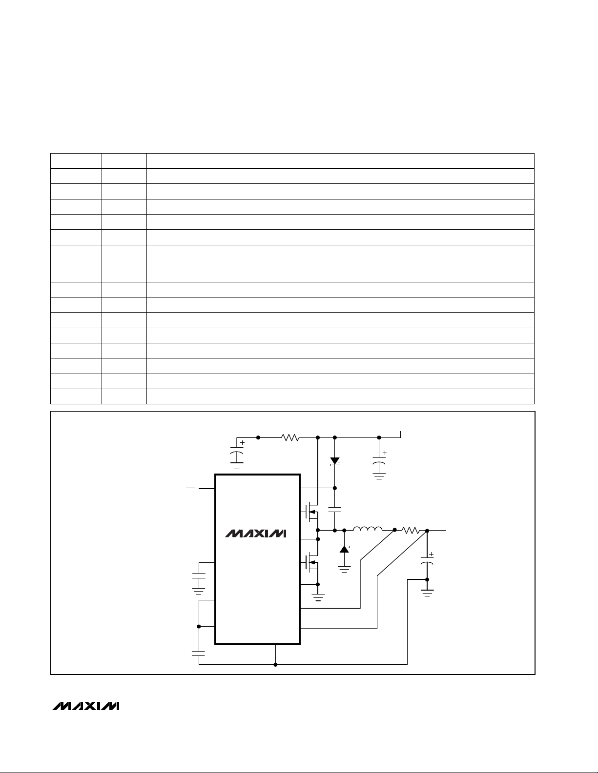
Figure 1. Standard Application Circuit
R2
INPUT
4.5V TO 5.5V
SHUTDOWN
ON/OFF
C5
(OPTIONAL)
C6
0.22µF
0.01µF
4.7µF
C4
ON
SS
SYNC
REF
V
CC
MAX767
GND
10
BST
PGND
Ω
DH
LX
DL
CS
FB
D1
SMALLSIGNAL
SCHOTTKY
C3
N1
0.1µF
D2
N2
C1
OUTPUT
L1
R1
3.3V
C2
Page 6

MAX767
_____Standard Application Circuits
This data sheet shows five predesigned circuits with
output current capabilities from 1.5A to 10A. Many
users will find one of these standard circuits appropriate for their needs. If a standard circuit is used, the
remainder of this data sheet (Detailed Description and
Applications Information and Design Procedure) can
be bypassed.
Figure 1 shows the Standard Application Circuit. Table 1
gives component values and part numbers for five different implementations of this circuit: 1.5A, 3A, 5A, 7A,
and 10A output currents.
Each of these circuits is designed to deliver the full
rated output load current over the temperature range
listed. In addition, each will withstand a short circuit of
several seconds duration from the output to ground. If
the circuit must withstand a continuous short circuit,
refer to the Short-Circuit Duration section for the
required changes.
Layout and Grounding
Good layout is necessary to achieve the designed output power, high efficiency, and low noise. Good layout
includes the use of a ground plane, appropriate component placement, and correct routing of traces using
appropriate trace widths. The following points are in
order of decreasing importance.
1. A ground plane is essential for optimum performance. In most applications, the circuit will be
located on a multilayer board and full use of the four
or more copper layers is recommended. Use the
top and bottom layers for interconnections and the
inner layers for an uninterrupted ground plane.
2. Because the sense resistance values are similar to
a few centimeters of narrow traces on a printed circuit board, trace resistance can contribute significant errors. To prevent this, Kelvin connect CS and
FB to the sense resistor; i.e., use separate traces
not carrying any of the inductor or load current, as
shown in Figure 2. These signals must be carefully
shielded from DH, DL, BST, and the LX node.
Important: place the sense resistor as close as possible to and no further than 10mm from the MAX767.
3. Place the LX node components N1, N2, L1, and D2
as close together as possible. This reduces resistive and switching losses and confines noise due to
ground inductance.
4. The input filter capacitor C1 should be less than
10mm away from N1’s drain. The connecting copper trace carries large currents and must be at least
2mm wide, preferably 5mm.
5. Keep the gate connections to the MOSFETs short
for low inductance (less than 20mm long and more
than 0.5mm wide) to ensure clean switching.
6. To achieve good shielding, it is best to keep all
switching signals (MOSFET gate drives DH and DL,
BST, and the LX node) on one side of the board
and all sensitive nodes (CS, FB, and REF) on the
other side.
7. Connect the GND and PGND pins directly to the
ground plane, which should ideally be an inner
layer of a multilayer board.
_______________Detailed Description
Note: The remainder of this document contains the
detailed information necessary to design a circuit that
differs substantially from the five standard application
circuits. If you are using one of the predesigned standard circuits, the following sections are provided only
for your reading pleasure.
The MAX767 converts a 4.5V to 5.5V input to a 3.3V
output. Its load capability depends on external components and can exceed 10A. The 3.3V output is generated by a current-mode, pulse-width-modulation (PWM)
step-down regulator. The PWM regulator operates at
either 200kHz or 300kHz, with a corresponding tradeoff between somewhat higher efficiency (200kHz) and
smaller external component size (300kHz). The
MAX767 also has a 3.3V, 5mA reference voltage. Faultprotection circuitry shuts off the output should the reference lose regulation or the input voltage go below 4V
(nominally).
External components for the MAX767 include two Nchannel MOSFETs, a rectifier, and an LC output filter.
The gate-drive signal for the high-side MOSFET, which
must exceed the input voltage, is provided by a boost
circuit that uses a 0.1µF capacitor. The synchronous
rectifier keeps efficiency high by clamping the voltage
across the rectifier diode. An external low-value current-sense resistor sets the maximum current limit, preventing excessive inductor current during start-up or
under short-circuit conditions. An optional external
capacitor sets the programmable soft-start, reducing
in-rush surge currents upon start-up and providing
adjustable power-up time.
The PWM regulator is a direct-summing type, lacking a
traditional integrator-type error amplifier and the phase
shift associated with it. It therefore does not require
external feedback-compensation components, as long
as you follow the ESR guidelines in the Applications
Information and Design Procedure sections.
5V-to-3.3V, Synchronous, Step-Down
Power-Supply Controller
6 _______________________________________________________________________________________
Page 7

MAX767
5V-to-3.3V, Synchronous, Step-Down
Power-Supply Controller
_______________________________________________________________________________________ 7
Part 1.5A Circuit 3A Circuit 5A Circuit 7A Circuit 10A Circuit
L1
10µH
Sumida CDR74B-100
5µH
Sumida CDR125
DRG# 4722-JPS-001
3.3µH
Coilcraft
DO3316-332
2.1µH, 5mΩ
Coiltronics
CTX03-12338-1
1.5µH, 3.5mΩ
Coiltronics
CTX03-12357-1
R1
0.04Ω
IRC LR2010-01-R040
or DD WSL-2512-R040
0.02Ω
IRC LR2010-01-R020
or DD WSL-2512-R020
0.012Ω
DD WSL-2512-R012
or 2 x 0.025Ω
IRC LR2010-01-R025
(in parallel)
3 x 0.025Ω
IRC LR2010-01-R025
or DD WSL-2512-R025
(in parallel)
3 x 0.020Ω
IRC LR2010-01-R020
or 2 x 0.012Ω
DD WSL-2512-R012
(in parallel)
N1,
N2
International
Rectifier IRF7101,
Siliconix Si9936DY
or Motorola
MMDF3N03HD
(dual N-channel)
Siliconix Si9410DY,
International
Rectifier IRF7101
or Motorola
MMDF3N03HD
(both FETs in parallel)
Motorola
MTD20N03HDL
Motorola
MTD75N03HDL
(N1)
MTD20N03HDL
(N2)
Motorola
MTD75N03HDL
C1
47µF, 20V
AVX TPSD476K020R
2 x 47µF, 20V
AVX TPSD476K020R
220µF, 10V
Sanyo
OS-CON 10SA220M
2 x 100µF, 10V
Sanyo
OS-CON 10SA100M
2 x 220µF, 10V
Sanyo
OS-CON 10SA220M
C2
220µF, 6.3V
Sprague
595D227X06R3D2B
2 x 150µF, 10V
Sprague
595D157X0010D7T
2 x 220µF, 10V
Sanyo
OS-CON 10SA220M
2 x 220µF, 10V
Sanyo
OS-CON 10SA220M
4 x 220µF, 10V
Sanyo
OS-CON 10SA220M
D2
1N5817
Nihon EC10QS02,
or Motorola
MBRS120T3
1N5817
Nihon EC10QS02,
or Motorola
MBRS120T3
1N5820
Nihon NSQ03A02,
or Motorola
MBRS340T3
1N5820
Nihon NSQ03A02,
or Motorola
MBRS340T3
1N5820
Nihon NSQ03A02,
or Motorola
MBRS340T3
Temp.
Range
to +85°C to +85°C to +85°C to +85°C to +85°C
Table 1. Component Values
Table 2. Component Suppliers
Company Factory Fax [Country Code] USA Telephone
AVX [1] (803) 626-3123
(803) 946-0690
(800) 282-4975
Coilcraft [1] (847) 639-1469 (847) 639-6400
Coiltronics [1] (561) 241-9339 (561) 241-7876
DD [1] (402) 563-6418 (402) 564-3131
IRC [1] (512) 992-3377 (512) 992-7900
International
Rectifier
[1] (310) 322-3332 (310) 322-3331
Nihon [81] 3-3494-7414 (805) 867-2555
Sanyo [81] 7-2070-1174 (619) 661-6835
Siliconix [1] (408) 970-3950 (408) 988-8000
Sprague [1] (603) 224-1430 (603) 224-1961
Sumida [81] 3-3607-5144 (847) 956-0666
Motorola [1] (602) 994-6430 (602) 303-5454
Page 8

MAX767
The main gain block is an open-loop comparator that
sums four signals: output voltage error signal, currentsense signal, slope-compensation ramp, and the 3.3V
reference. This direct-summing method approaches
the ideal of cycle-by-cycle control of the output voltage.
Under heavy loads, the controller operates in full PWM
mode. Every pulse from the oscillator sets the output
latch and turns on the high-side switch for a period
determined by the duty factor (approximately
V
OUT
/ VIN).
As the high-side switch turns off, the synchronous rectifier latch is set; 60ns later, the low-side switch turns on.
The low-side switch stays on until the beginning of the
next clock cycle (in continuous-conduction mode) or
until the inductor current reaches zero (in discontinuous-conduction mode). Under fault conditions where
the inductor current exceeds the 100mV current-limit
threshold, the high-side latch resets and the high-side
switch turns off.
At light loads, the inductor current fails to exceed the
25mV threshold set by the minimum-current comparator. When this occurs, the PWM goes into Idle-Mode™,
skipping most of the oscillator pulses to reduce the
switching frequency and cut back switching losses.
The oscillator is effectively gated off at light loads
because the minimum-current comparator immediately
resets the high-side latch at the beginning of each
cycle, unless the FB signal falls below the reference
voltage level.
Soft-Start
Connecting a capacitor from the soft-start pin (SS) to
ground allows a gradual build-up of the 3.3V output
after power is applied or ON is driven high. When ON is
low, the soft-start capacitor is discharged to GND.
When ON is driven high, a 4µA constant current source
charges the capacitor up to 4V. The resulting ramp voltage on SS linearly increases the current-limit comparator set-point, increasing the duty cycle to the external
power MOSFETs. With no soft-start capacitor, the full
output current is available within 10µs (see Applications
Information and Design Procedure section).
Synchronous Rectifier
Synchronous rectification allows for high efficiency by
reducing the losses associated with the Schottky rectifier. Also, the synchronous-rectifier MOSFET is necessary for correct operation of the MAX767’s boost gatedrive supply.
When the external power MOSFET (N1) turns off, energy stored in the inductor causes its terminal voltage to
reverse instantly. Current flows in the loop formed by
the inductor (L1), Schottky diode (D2), and the load—
an action that charges up the output filter capacitor
(C2). The Schottky diode has a forward voltage of
about 0.5V which, although small, represents a significant power loss and degrades efficiency. The synchronous-rectifier MOSFET parallels the diode and is turned
on by DL shortly after the diode conducts. Since the
synchronous rectifier’s on resistance (r
DS(ON)
) is very
low, the losses are reduced. The synchronous-rectifier
MOSFET is turned off when the inductor current falls to
zero.
The MAX767’s internal break-before-make timing
ensures that shoot-through (both external switches
turned on at the same time) does not occur. The
Schottky rectifier conducts during the time that neither
MOSFET is on, which improves efficiency by preventing
the synchronous-rectifier MOSFET’s lossy body diode
from conducting.
The synchronous rectifier works under all operating
conditions, including discontinuous-conduction mode
and idle-mode.
5V-to-3.3V, Synchronous, Step-Down
Power-Supply Controller
8 _______________________________________________________________________________________
Figure 2. Kelvin Connections for the Current-Sense Resistor
Idle-Mode is a trademark of Maxim Integrated Products.
FAT, HIGH-CURRENT TRACES
MAIN CURRENT PATH
SENSE RESISTOR
MAX767
Page 9

MAX767
5V-to-3.3V, Synchronous, Step-Down
Power-Supply Controller
_______________________________________________________________________________________ 9
Figure 3. MAX767 Block Diagram
2.8V
CS
1X
MAIN PWM
COMPARATOR
MINIMUM
CURRENT
(IDLE-MODE)
3.3V
N
60kHz
LPF
30R
R
Q
S
V
CC
CURRENT
LIMIT
0mV TO 100mV
200kHz/300kHz
OSCILLATOR
1R
ON
LEVEL
SHIFT
SHOOTTHROUGH
CONTROL
V
REF
CC
+3.3V
REFERENCE
SLOPE COMP
4V
25mV
4µA
FAULT
SS
ON
FB
BST
DH
LX
MAX767
SYNCHRONOUS
RECTIFIER CONTROL
V
R
Q
S
SYNC
LEVEL
SHIFT
CC
DL
PGND
Page 10

MAX767
Gate-Driver Boost Supply
Gate-drive voltage for the high-side N-channel switch is
generated with the flying-capacitor boost circuit shown
in Figure 4. The capacitor (C3) is alternately charged
from the 5V input via the diode (D1) and placed in parallel with the high-side MOSFET’s gate-source terminals. On start-up, the synchronous rectifier (low-side)
MOSFET (N2) forces LX to 0V and charges the BST
capacitor to 5V. On the second half-cycle, the PWM
turns on the high-side MOSFET (N1); it does this by
closing an internal switch between BST and DH, which
connects the capacitor to the MOSFET gate. This provides the necessary enhancement voltage to turn on
the high-side switch, an action that “boosts” the 5V
gate-drive signal above the input voltage.
Ringing seen at the high-side MOSFET gates (DH) in
discontinuous-conduction mode (light loads) is a natural operating condition. It is caused by the residual
energy in the tank circuit, formed by the inductor and
stray capacitance at the LX node. The gate-driver negative rail is referred to LX, so any ringing there is directly coupled to the gate-drive supply.
Modes of Operation
PWM Mode
Under heavy loads—over approximately 25% of full
load—the supply operates as a continuous-current
PWM supply (see Typical Operating Characteristics).
The duty cycle, %ON, is approximately:
V
OUT
%ON = ________
V
IN
Current flows continuously in the inductor: first, it ramps
up when the power MOSFET conducts; second, it
ramps down during the flyback portion of each cycle as
energy is put into the inductor and then discharged into
the load. Note that the current flowing into the inductor
when it is being charged is also flowing into the load,
so the load is continuously receiving current from the
inductor. This minimizes output ripple and maximizes
inductor use, allowing very small physical and electrical
sizes. Output ripple is primarily a function of the filter
capacitor’s effective series resistance (ESR), and is
typically under 50mV (see Design Procedure section).
Idle-Mode
Under light loads (<25% of full load), the MAX767
enhances efficiency by turning the drive voltage on and
off for only a single clock period, skipping most of the
clock pulses entirely. Asynchronous switching, seen as
“ghosting” on an oscilloscope, is thus a normal operating condition whenever the load current is less than
approximately 25% of full load.
At certain input voltage and load conditions, a transition
region exists where the controller can pass back and
forth from idle-mode to PWM mode. In this situation,
short pulse bursts occur, which make the current waveform look erratic but do not materially affect the output
ripple. Efficiency remains high.
Current Limiting
The voltage between CS and FB is continuously monitored. An external, low-value shunt resistor is connected between these pins, in series with the inductor,
allowing the inductor current to be continuously measured throughout the switching cycle. Whenever this
voltage exceeds 100mV, the drive voltage to the external high-side MOSFET is cut off. This protects the MOSFET, the load, and the input supply in case of short circuits or temporary load surges. The current-limiting
resistance is typically 20mΩ for 3A.
5V-to-3.3V, Synchronous, Step-Down
Power-Supply Controller
10 ______________________________________________________________________________________
Figure 4. Boost Supply for High-Side Gate Driver
V
MAX767
V
CC
LEVEL
TRANSLATOR
PWM
BST
DH
LX
V
CC
DL
D1
C3
N1
L1
N2
IN
C1
Page 11

Oscillator Frequency
The SYNC input controls the oscillator frequency.
Connecting SYNC to GND or to VCCselects 200kHz
operation; connecting it to REF selects 300kHz operation. SYNC can also be driven with an external 240kHz
to 350kHz CMOS/TTL source to synchronize the internal oscillator. Normally, 300kHz operation is chosen to
minimize the inductor and output filter capacitor sizes,
but 200kHz operation may be chosen for a small (about
1%) increase in efficiency at heavy loads.
Internal Reference
The internal 3.3V bandgap reference (REF) remains
active, even when the switching regulator is turned off.
It can furnish up to 5mA, and can be used to supply
memory keep-alive power or for other purposes.
Bypass REF to GND with 0.22µF, plus 1µF/mA of load
current.
Applications Information and
__________________Design Procedure
Most users will be able to work with one of the standard
application circuits; others may want to implement a
circuit with an output current rating that lies between or
beyond the standard values.
If you want an output current level that lies between two
of the standard application circuits, you can interpolate
many of the component values from the values given
for the two circuits. These components include the
input and output filter capacitors, the inductor, and the
sense resistor. The capacitors must meet ESR and ripple current requirements (see Input Filter Capacitor and
Output Filter Capacitor sections). The inductor must
meet the required current rating (see Inductor section).
You may use the rectifier and MOSFETs specified for
the circuit with the greater output current capability, or
choose a new rectifier and MOSFETs according to the
requirements detailed in the Rectifier and MOSFET
Switches sections. For more complete information, or
for output currents in excess of 10A, refer to the design
information in the following sections.
Inductor, L1
Three inductor parameters are required: the inductance
value (L), the peak inductor current (I
LPEAK
), and the
coil resistance (RL). The inductance is:
1.32
L1 = ______________
f x I
OUT
x LIR
where:
f = switching frequency, normally 300kHz
I
OUT
= maximum 3.3V DC load current (A)
LIR = ratio of inductor peak-to-peak AC
current to average DC load current,
typically 0.3.
A higher LIR value allows smaller inductance, but
results in higher losses and ripple.
The highest peak inductor current (I
LPEAK
) equals the
DC load current (I
OUT
) plus half the peak-to-peak AC
inductor current (I
LPP
). The peak-to-peak AC inductor
current is typically chosen as 30% of the maximum DC
load current, so the peak inductor current is 1.15 x I
OUT
.
The peak inductor current at any load is given by:
1.32
I
LPEAK
= I
OUT
+ __________
2 x f x L1
The coil resistance should be as low as possible,
preferably in the low milliohms. The coil is effectively in
series with the load at all times, so the wire losses alone
are approximately:
Power Loss = I
OUT
2
x R
L
In general, select a standard inductor that meets the L,
I
LPEAK
, and RLrequirements. If a standard inductor is
unavailable, choose a core with an LI2parameter
greater than L x I
LPEAK
2
, and use the largest wire that
will fit the core.
Current-Sense Resistor, R1
The current-sense resistor must carry the peak current
in the inductor, which exceeds the full DC load current.
The internal current limiting starts when the voltage
across the sense resistors exceeds 100mV nominally,
80mV minimum. Use the minimum value to ensure adequate output current capability: R1 = 80mV / I
LPEAK
.
The low VIN/V
OUT
ratio creates a potential problem with
start-up under full load or with load transients from noload to full load. If the supply is subjected to these conditions, reduce the sense resistor:
70mV
R1 = ———
I
LPEAK
Since the sense-resistance values are similar to a few
centimeters of narrow traces on a printed circuit board,
trace resistance can contribute significant errors. To
prevent this, Kelvin connect the CS and FB pins to the
sense resistors; i.e., use separate traces not carrying
any of the inductor or load current, as shown in Figure 2.
MAX767
5V-to-3.3V, Synchronous, Step-Down
Power-Supply Controller
______________________________________________________________________________________ 11
Page 12

MAX767
Place R1 as close as possible to the MAX767, preferably less than 10mm. Run the traces at minimum spacing from one another. If they are longer than 20mm,
bypass CS to FB with a 1nF capacitor placed as close
as possible to these pins. The wiring layout for these
traces is critical for stable, low-ripple outputs (see
Layout and Grounding section).
Input Filter Capacitor, C1
Use at least 6µF per watt of output power for C1. If the
5V input is some distance away or comes through a PC
bus, greater capacitance may be desirable to improve
the load-transient response. Use a low-ESR capacitor
located no further than 10mm from the MOSFET switch
(N1) to prevent ringing. The ripple current rating must
be at least I
RMS
= 0.5 x I
OUT
. For high-current applications, two or more capacitors in parallel may be needed
to meet these requirements.
The ESR of C1 is effectively in series with the input. The
resistive dissipation of C1, I
RMS
2
x ESRC1, can signifi-
cantly impact the circuit’s efficiency.
Output Filter Capacitor, C2
The output filter capacitor determines the loop stability,
output voltage ripple, and output load-transient
response.
Stability
To ensure stability, stay above the minimum capacitance value and below the maximum ESR value. These
values are:
3Ω
C2 > —— µF
R1
and
ESR
C2
< R1
Be sure to satisfy both these requirements. To achieve
the low ESR required, it may be appropriate to parallel
two or more capacitors and/or use a total capacitance
2 or 3 times larger than the calculated minimum.
Output Ripple
The output ripple in continuous-conduction mode is:
V
OUT(RPL)
= I
OUT
(max) x LIR x
1
(ESR
C2
+ ———————)
2 x π x f x C2
where f is the switching frequency (200kHz or 300kHz).
In idle-mode, the ripple has a capacitive and a resistive
component:
.
0.0004 x L
V
OUT(RPL)
(C) = _____________ x 0.89 Volts
R12x C2
0.02 x ESR
C2
V
OUT(RPL)
(R) = _____________
R1
The total ripple, V
OUT(RPL)
, can be approximated as
follows:
if
V
OUT(RPL)
(R) < 0.5 V
OUT(RPL)
(C)
then
V
OUT(RPL)
= V
OUT(RPL)
(C)
otherwise
V
OUT(RPL)
= 0.5 V
OUT(RPL)
(C) +
V
OUT(RPL)
(R)
Load-Transient Performance
In response to a large step increase in load current, the
output voltage will sag for several microseconds unless
C2 is increased beyond the values that satisfy the
above requirements. Note that an increase in capacitance is all that’s required to improve the transient
response, and that the ESR requirements don’t change.
Therefore, the added capacitance can be supplied by
an additional low-cost bulk capacitor in parallel with the
normal low-ESR switching-regulator capacitor. The
equation for voltage sag under a step load change is:
I
STEP
2
x L
V
SAG
= ________________________________
2 x C2 x (VIN(min) x DMAX - 3.3V)
where DMAX is the maximum duty cycle. Higher duty
cycles are possible when the oscillator frequency is
reduced to 200kHz, since fixed propagation delays
through the PWM comparator become a lesser part of
the whole period. The tested worst-case limit for DMAX
is 92% at 200kHz or 89% at 300kHz. Lower inductance
values can reduce the filter capacitance requirement,
but only at the expense of increased output ripple (due
to higher peak currents).
5V-to-3.3V, Synchronous, Step-Down
Power-Supply Controller
12 ______________________________________________________________________________________
Page 13

RC Filter for V
CC
R2 and C4 form a lowpass filter to remove switching
noise from the V
CC
input to the MAX767. C4 must have
fairly low ESR (<5Ω). Switching noise can interfere with
proper output voltage regulation, resulting in an excessive output voltage decrease (>100mV) at full load.
Overheating during soldering can damage the surfacemount capacitors specified for C4, causing the regulation problems described above. Take care to heat the
capacitor for as short a time as possible, especially if it
is soldered by hand.
Rectifier, D2
Use a 1N5817 or similar Schottky diode for applications
up to 3A, or a 1N5820 for up to 10A. Surface-mount
equivalents are available from N.I.E.C. with part numbers EC10QS02 and NSQ03A02, or from Motorola with
part numbers MBRS120T3 and MBRS320T3. D2 must
be a Schottky diode to prevent the lossy MOSFET body
diode from turning on.
Soft-Start
A capacitor connected from GND to SS causes the
supply’s current-limit level to ramp up slowly. The ramp
time to full current limit is approximately 1ms for every
nF of capacitance on SS, with a minimum value of
10µs. Typical values for the soft-start capacitor are in
the 10nF to 100nF range; a 5V rating is sufficient.
The time required for the output voltage to ramp up to
its rated value depends upon the output load, and is
not necessarily the same as the time it takes for the current limit to reach full capacity.
Duty Cycle
The duty cycle for the high-side MOSFET (N1) in continuous-conduction mode is:
100% x ( V
OUT
+ VN2)
___________________
V
IN
- V
N1
where:
V
OUT
= 3.3V
VIN= 5V
VN1and VN2= I
LOAD
x r
DS(ON)
for each MOSFET.
It is apparent that, in continuous-conduction mode, N1
will conduct for about twice the time as N2. Under shortcircuit conditions, however, N2 can conduct as much
90% of the time. If there is a significant chance of short
circuiting the output, select N2 to handle the resulting
duty cycle (see Short-Circuit Duration section).
MOSFET Switches, N1 and N2
The two N-channel MOSFETs must be “logic-level”
FETs; that is, they must be fully on (have low
r
DS(ON)
) with only 4V gate-source drive voltage. For
high-current applications, FETs with low gatethreshold voltage specifications (i.e., maximum
V
GS(TH)
= 2V rather than 3V) are preferred. In addition, they should have low total gate charge (<70nC)
to minimize switching losses.
For output currents in excess of the five standard application circuits, placing MOSFETs with very low gate
charge in parallel increases output current and lowers
resistive losses. N2 does not normally require the same
current capacity as N1 because it conducts only about
33% of the time, while N1 conducts about 66% of the
time.
Short-Circuit Duration
At their highest rated temperatures (+70°C or +85°C),
each of the five standard application circuits will withstand a short circuit of several seconds duration. In
most cases, the MAX767 will be used in applications
where long-term short circuiting of the output is unlikely.
If it is desirable for the circuit to withstand a continuous
short circuit, the MOSFETs must be able to dissipate
the required power. This depends on physical factors
such as the mounting of the transistor, any heatsinking used, and ventilation provided, as well as the
actual current the transistor must deliver. The shortcircuit current is approximately 100mV / R1, but may
vary by ±20%.
Cautious design requires that the transistors
withstand the maximum possible current, which is
ISC= 120mV / R1. N1 and N2 must withstand this
current scaled by their maximum duty factors. The
maximum duty factor for N1 occurs under highload (but not short-circuit) conditions, and is approximately V
OUT
/ VIN(min) or about 0.7. The maximum duty factor for N2 occurs during short-circuit
conditions and is:
ISCx r
DS(ON)N2
1 - —————————————
VIN(max) - ISCx r
DS(ON)N1
which can exceed 0.9. The total power dissipated in
both MOSFETs together is I
SC
2
x r
DS(ON)
.
MAX767
5V-to-3.3V, Synchronous, Step-Down
Power-Supply Controller
______________________________________________________________________________________ 13
Page 14

MAX767
Proper circuit operation requires that the short-circuit
current be at least I
LOAD
x (1 + LIR / 2). However, the
standard application circuits are designed for a shortcircuit current slightly in excess of this amount. This
excess design current guarantees proper start-up
under constant full-load conditions and proper full-load
transient response, and is particularly necessary with
low input voltages. If the circuit will not be subjected to
full-load transients or to loads approaching the full-load
at start-up, you can decrease the short-circuit current
by increasing R1, as described in the Current-Sense
Resistor section. This may allow use of MOSFETs with a
lower current-handling capability.
Heavy-Load Efficiency
Losses due to parasitic resistances in the switches,
coil, and sense resistor dominate at high load-current
levels. Under heavy loads, the MAX767 operates deep
in the continuous-conduction mode, where there is a
large DC offset to the inductor current (plus a small
sawtooth AC component) (see Inductor section). This
DC current is exactly equal to the load current, a fact
which makes it easy to estimate resistive losses via the
simplifying assumption that the total inductor current is
equal to this DC offset current. The major loss mechanisms under heavy loads, in usual order of importance,
are:
•I2R losses
• gate-charge losses
• diode-conduction losses
• transition losses
• capacitor-ESR losses
• losses due to the operating supply current of the IC.
Inductor-core losses, which are fairly low at heavy
loads because the AC component of the inductor current is small, are not accounted for in this analysis.
P
OUT
Efficiency = ______ x 100% =
P
IN
POUT
_______________ x 100%
P
OUT
+ PD
TOTAL
PD
TOTAL
= PD
(I2R)
+ PD
GATE
+ PD
DIODE
+
PD
TRAN
+ PD
CAP
+ PD
IC
I2R Losses
PD
(I2R)
= resistive loss = (I
LOAD
2
) x
(R
COIL
+ r
DS(ON)
+ R1)
where R
COIL
is the DC resistance of the coil and
r
DS(ON)
is the drain-source on resistance of the MOS-
FET. Note that the r
DS(ON)
term assumes that identical
MOSFETs are employed for both the synchronous rectifier and high-side switch, because they time-share the
inductor current. If the MOSFETs are not identical, estimate losses by averaging the two individual r
DS(ON)
terms according to their duty factors: 0.66 for N1 and
0.34 for N2.
Gate-Charge Losses
PD
GATE
= gate driver loss = qGx f x 5V
where qGis the sum of the gate charge for low- and
high-side switches. Note that gate-charge losses are
dissipated in the IC, not the MOSFETs, and therefore
contribute to package temperature rise. For a pair of
matched MOSFETs, qGis simply twice the gate capacitance of a single MOSFET (a data sheet specification).
Diode Conduction Losses
PD
DIODE
= diode conduction losses =
I
LOAD
x VDx tDx f
where VDis the forward voltage of the Schottky diode
at the output current, tDis the diode’s conduction time
(typically 110ns), and f is the switching frequency.
Transition Losses
PD
TRAN
= transition loss =
V
IN
2
x C
RSS
x I
LOAD
x f
______________________
I
DRIVE
where C
RSS
is the reverse transfer capacitance of the
high-side MOSFET (a data sheet parameter), f is the
switching frequency, and I
DRIVE
is the peak current
available from the high-side gate driver output (approximately 1A).
Additional switching losses are introduced by other
sources of stray capacitance at the switching node,
including the catch-diode capacitance, coil interwinding capacitance, and low-side switch drain capacitance, and are given as PDSW= V
IN
2
x C
STRAY
x f, but
these are usually negligible compared to C
RSS
losses.
The low-side switch introduces only tiny switching losses, since its drain-source voltage is already low when it
turns on.
5V-to-3.3V, Synchronous, Step-Down
Power-Supply Controller
14 ______________________________________________________________________________________
Page 15

Capacitor ESR Losses
PD
CAP
= capacitor ESR loss = I
RMS
2
x ESR
where I
RMS
= RMS AC input current, approximately
I
LOAD
/ 2.
Note that losses in the output filter capacitors are small
when the circuit is heavily loaded, because the current
into the capacitor is not chopped. The output capacitor
sees only the small AC sawtooth ripple current. Ensure
that the input bypass capacitor has a ripple current rating that exceeds the value of I
RMS
.
IC Supply-Current Losses
PDICis the quiescent power dissipation of the IC and is
5V times the quiescent supply current (a data sheet
parameter), or about 5mW.
Light-Load Efficiency
Under light loads, the PWM will operate in discontinuous-conduction mode, where the inductor current discharges to zero at some point during each switching
cycle. New loss mechanisms, insignificant at heavy
loads, begin to become important. The basic difference
is that in discontinuous mode, the AC component of the
inductor current is large compared to the load current.
This increases losses in the core and in the output filter
capacitors. Ferrite cores are recommended over powdered-material types for best light-load efficiency.
At light loads, the inductor delivers triangular current
pulses rather than the nearly square waves found in
continuous-conduction mode. These pulses ramp up to
a point set by the idle-mode current comparator, which
is internally fixed at approximately 25% of the full-scale
current-limit level. This 25% threshold provides an optimum balance between low-current efficiency and output voltage noise (the efficiency curve would actually
look better with this threshold set at about 45%, but the
output noise would be too high).
____Additional Application Circuits
High-Accuracy Power Supplies
The standard application circuit’s accuracy is dominated by reference voltage error (±1.8%) and load regulation error (-2.5%). Both of these parameters can be
improved as shown in Figures 5 and 6. Both circuits
rely on an external integrator amplifier to increase the
DC loop gain in order to reduce the load regulation
error to 0.1%. Reference error is improved in the first
circuit by employing a version of the MAX767 (“T”
grade) which has a ±1.2% reference voltage tolerance.
Reference error of the second circuit is further
improved by substituting a highly accurate external reference chip (MAX872), which contributes ±0.38% total
error over temperature.
These two circuits were designed with the latest generation of dynamic-clock µPs in mind, which place great
demands on the transient-response performance of the
power supply. As the µP clock starts and stops, the
load current can change by several amps in less than
100ns. This tremendous ∆i/∆t can cause output voltage
overshoot or sag that results in the CPU VCC going out
of tolerance unless the power supply is carefully
designed and located close to the CPU. These circuits
have excellent dynamic response and low ripple, with
transient excursions of less than 40mV under zero to
full-load step change. In particular, these two circuits
support the “VR” (voltage regulator) version of the Intel
P54C Pentium™ CPU, which requires that its supply
voltage, including noise and transient errors, be within
the 3.30V to 3.45V range.
To configure these circuits for a given load current
requirement, substitute standard components from
Table 1 for the power switching elements (N1, N2, L1,
C1, C2) or use the Design Procedure. R1 can also be
taken from Table 1, but must be adjusted approximately 10% higher in order to maintain the correct currentlimit threshold. This increased value is due to the 0.9
gain factor introduced by the H-bridge resistor divider
(R3–R6).
If the remote sense line must sense the output voltage
on the far side of a connector or jumper that has the
possibility of becoming disconnected while the power
supply is operating, an additional 10kΩ resistor should
connect the sense line to the output voltage in the connector’s power-supply side in order to prevent accidental overvoltage at the CPU.
For applications that are powered from a fixed +12V or
battery input rather than from +5V, use a MAX797 IC
instead of the MAX767. The MAX797 is capable of
accepting inputs up to 30V. See the MAX796–MAX799
data sheet for a high-accuracy circuit schematic.
MAX767
5V-to-3.3V, Synchronous, Step-Down
Power-Supply Controller
______________________________________________________________________________________ 15
Page 16

MAX767
5V-to-3.3V, Synchronous, Step-Down
Power-Supply Controller
16 ______________________________________________________________________________________
Figure 5. High-Accuracy CPU Power Supply with Internal Reference
INPUT
4.75V TO 5.5V
R2
Ω
10
C4
4.7µF
SHUTDOWN
ON/OFF
V
CC
ON
C10
0.01µF
(OPTIONAL)
MAX767T
SS
GND
DH
BST
PGND
CS
REF
SYNC
V
0.01µF
V
CC
OUT
C5
C8
620pF
MAX495
D1
N1
C3
0.1µF
LX
DL
FB
N2
R8
10k
C9
0.22µF
R9
332k, 1%
C1
L1
D2
TO MAX767
= V
REF
(
R10
+ 1
R9
R3
1k,
1%
R7
330k
R5
10k,
1%
R10
8.06k, 1%
)
3.38V OUTPUT
R11
5.1k
MIN
LOAD
3.427V MAX
3.330V MIN
C7
10µF CERAMIC
(LOCATE AT
µ
P PINS)
C2R1
R4
1k,
1%
C6
0.01µF
R6
10k,
1%
REMOTE SENSE LINE
Page 17

MAX767
5V-to-3.3V, Synchronous, Step-Down
Power-Supply Controller
______________________________________________________________________________________ 17
Figure 6. High-Accuracy CPU Power Supply with External Reference
INPUT
4.75V TO 5.5V
R2
Ω
20
C4
22µF
SHUTDOWN
ON/OFF
0.22µF
V
ON
REF
SYNC
C10
0.01µF
(OPTIONAL)
R10
= V
REF
(
R9
R3
1k,
1%
330k
R5
10k,
1%
118k, 0.1%
+ 1
)
3.38V OUTPUT
R11
5.1k
MIN
LOAD
3.408V MAX
3.369V MIN
C7
10µF CERAMIC
(LOCATE AT
µ
P PINS)
C2R1
R4
1k,
1%
R7
R10
C6
0.01µF
R6
10k,
1%
REMOTE SENSE LINE
V
D1
C3
0.1µF
TO MAX767
V
CCC9
R8
10k
R9
332k, 0.1%
N1
N2
DH
GND
VIN
MAX872
GND
BST
LX
DL
PGND
CS
FB
VOUT
CC
MAX767
SS
C1
L1
D2
OUT
C5
0.01µF
C8
1000pF
MAX495
Page 18

MAX767
5V-to-3.3V, Synchronous, Step-Down
Power-Supply Controller
18 ______________________________________________________________________________________
___________________Chip TopographyOrdering Information (continued)
TRANSISTOR COUNT: 1294
SUBSTRATE CONNECTED TO GND
BST
GND
GND
REF
ON
GND
V
CC
0.181"
(4.597mm)
0.109"
(2.769mm)
GND
GND
GND
SYNC
PGND
V
CC
V
CC
V
CC
DL
LX
SS CS FB DH
3.3±1.2%20 SSOP-40°C to +85°CMAX767TEAP
3.6
3.45
3.3
V
OUT
(V)
±1.8%
±1.8%
±1.8%
REF
TOL
20 SSOP-40°C to +85°CMAX767SEAP
20 SSOP-40°C to +85°CMAX767REAP
20 SSOP-40°C to +85°CMAX767EAP
PINPACKAGE
TEMP. RANGEPART
Page 19

MAX767
5V-to-3.3V, Synchronous, Step-Down
Power-Supply Controller
______________________________________________________________________________________ 19
________________________________________________________Package Information
DIM
e
HE
A
A1
B
C
D
E
e
H
L
α
D
α
A
0.127mm
0.004in.
A1
B
C
L
INCHES MILLIMETERS
MIN
0.068
0.002
0.010
0.005
0.278
0.205
0.301
0.022
MAX
0.078
0.008
0.015
0.009
0.289
0.212
0.311
0.037
0˚
MIN
1.73
0.05
0.25
0.13
7.07
5.20
0.65 BSC0.0256 BSC
7.65
0.55
8˚
0˚
20-PIN PLASTIC
SHRINK
SMALL-OUTLINE
MAX
1.99
0.21
0.38
0.22
7.33
5.38
7.90
0.95
8˚
21-0003A
PACKAGE
 Loading...