

Page 1
19-0190; Rev 0; 9/93
3.3V, Step-Down,
Current-Mode PWM DC-DC Converters
__________________General Description
The MAX748A/MAX763A are 3.3V-output CMOS, stepdown switching regulators. The MAX748A accepts
inputs from 3.3V to 16V and delivers up to 500mA. The
MAX763A accepts inputs between 3.3V and 11V and
delivers up to 500mA. Typical efficiencies are 85% to
90%. Quiescent supply current is 1.4mA (MAX763A),
and only 0.2µA in shutdown.
Pulse-width-modulation (PWM) current-mode control provides precise output regulation and excellent transient
responses. Output voltage accuracy is guaranteed to be
±5% over line, load, and temperature variations.
Fixed-frequency switching allows easy filtering of output
ripple and noise, as well as the use of small external
components. A 22µH inductor works in most applications, so no magnetics design is necessary.
The MAX748A/MAX763A also feature cycle-by-cycle current limiting, overcurrent limiting, undervoltage lockout,
and programmable soft-start protection. The MAX748A
is available in 8-pin DIP and 16-pin wide SO packages;
the MAX763A comes in 8-pin DIP and SO packages.
___________________________Applications
5V-to-3.3V Converters
Cellular Phones
Portable Instruments
Hand-Held Computers
Computer Peripherals
________________________________Features
♦ Up to 500mA Load Currents
♦ Guaranteed 159kHz to 219.5kHz Current-Mode
PWM
♦ 85% to 90% Efficiencies
♦ 1.7mA Quiescent Current (MAX748A)
1.4mA Quiescent Current (MAX763A)
♦ 0.2µA Shutdown Supply Current
♦ 22µH Preselected Inductor Value;
No Component Design Required
♦ Overcurrent, Soft-Start, and Undervoltage
Lockout Protection
♦ Cycle-by-Cycle Current Limiting
♦ 8-Pin DIP/SO Packages (MAX763A)
_________________Ordering Information
PART TEMP. RANGE PIN-PACKAGE
MAX748ACPA 0°C to +70°C 8 Plastic DIP
MAX748ACWE 0°C to +70°C 16 Wide SO
MAX748AC/D 0°C to +70°C Dice*
MAX748AEPA -40°C to +85°C 8 Plastic DIP
MAX748AEWE -40°C to +85°C 16 Wide SO
MAX748AMJA -55°C to +125°C 8 CERDIP
Ordering Information continued on last page.
* Contact factory for dice specifications.
MAX748A/MAX763A
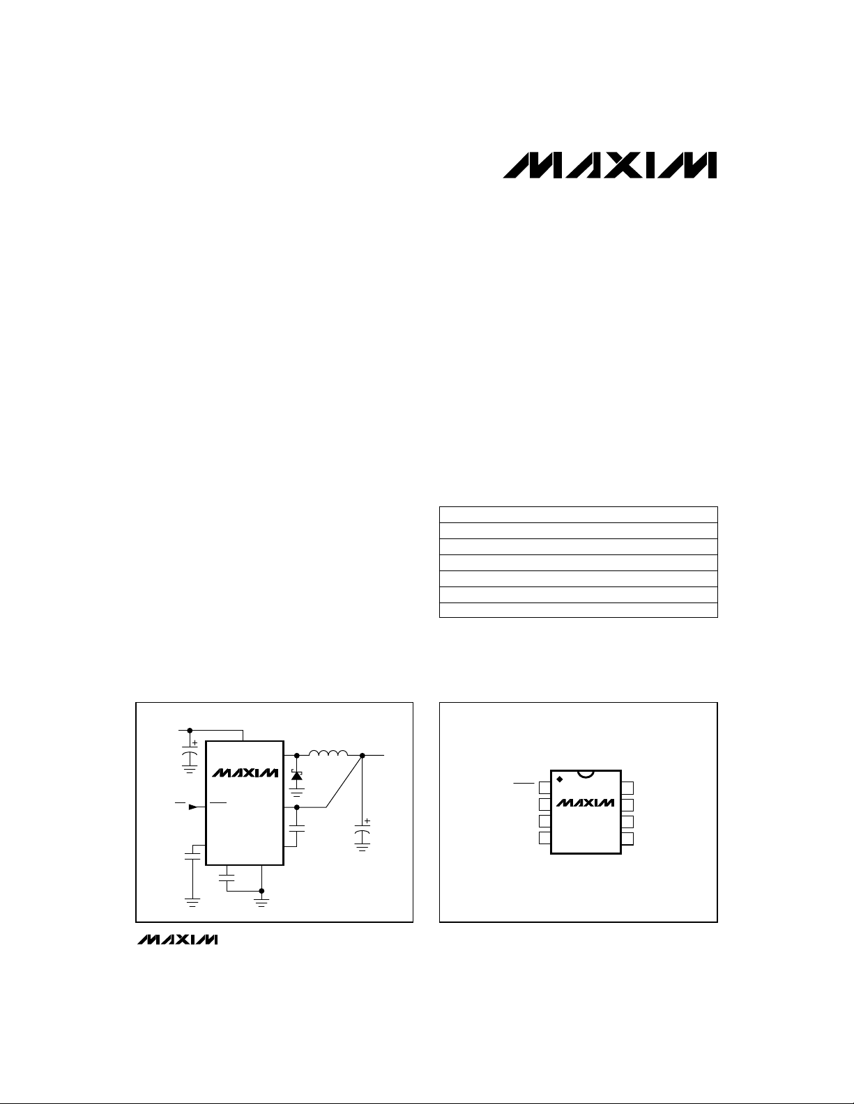
____________Typical Operating Circuit
INPUT
3.3V TO 16V
100µF
OUTPUT
3.3V
V+
LX
MAX748A
SHDNON/OFF
REF
OUT
CC
GNDSS
_______________________________________________________________________
22µH
____________________Pin Configurations
TOP VIEW
SHDN
1
REF
2
MAX748A
3
SS
MAX763A
4
CC
Pin Configurations continued on last page.
Maxim Integrated Products
Call toll free 1-800-998-8800 for free samples or literature.
DIP
V+
8
LX
7
GND
6
OUT
5
1
Page 2
3.3V, Step-Down,
Current-Mode PWM DC-DC Converters
ABSOLUTE MAXIMUM RATINGS
Pin Voltages:
V+ (MAX748A)......................................................+17V, -0.3V
V+ (MAX763A)......................................................+12V, -0.3V
LX (MAX748A) .................................(V+ - 21V) to (V+ + 0.3V)
LX (MAX763A) .................................(V+ - 12V) to (V+ + 0.3V)
OUT.................................................................................±25V
SHDN
SS, CC,
Peak Switch Current (I
Reference Current (I
Continuous Power Dissipation (T
8-Pin Plastic DIP (derate 6.90mW/°C above +70°C)...552mW
8-Pin SO (derate 5.88mW/°C above +70°C)...............471mW
Stresses beyond those listed under “Absolute Maximum Ratings” may cause permanent damage to the device. These are stress ratings only, and functional
operation of the device at these or any other conditions beyond those indicated in the operational sections of the specifications is not implied. Exposure to
absolute maximum rating conditions for extended periods may affect device reliability.
..........................................-0.3V to (V+ + 0.3V)
).....................................................2.0A
LX
)...................................................2.5mA
REF
= +70°C)
A
ELECTRICAL CHARACTERISTICS
(Circuit of Figure 3, V+ = 5V, I
MAX748A/MAX763A
PARAMETER CONDITIONS
Input Voltage Range 3.3 16.0 3.3 11.0 V
Output Voltage
Line Regulation 0.13 0.13 %/V
Load Regulation I
= 0mA, TA= T
LOAD
C/E temp. ranges,
V+ = 4.0V to 16V, 3.135 3.3 3.465
0mA < I
M temp. range,
V+ = 4.0V to 16V, 3.135 3.3 3.465
0mA < I
C/E temp. ranges,
V+ = 4.75V to 16V, 3.135 3.3 3.465
0mA < I
M temp. range,
V+ = 4.75V to 16V, 3.135 3.3 3.465
0mA < I
C/E temp. ranges,
V+ = 4.0V to 11V, 3.135 3.3 3.465
0mA < I
M temp. range,
V+ = 4.0V to 11V, 3.135 3.3 3.465
0mA < I
C/E temp. ranges,
V+ = 4.75V to 11V, 3.135 3.3 3.465
0mA < I
M temp. range,
V+ = 4.75V to 11V, 3.135 3.3 3.465
0mA < I
LOAD
< 300mA
LOAD
< 250mA
LOAD
< 500mA
LOAD
< 400mA
LOAD
< 300mA
LOAD
< 250mA
LOAD
< 500mA
LOAD
< 400mA
LOAD
= 0mA to 500mA 0.001 0.001 %/mA
MIN
to T
, unless otherwise noted.)
MAX
16-Pin Wide SO (derate 9.52mW/°C above +70°C)....762mW
8-Pin CERDIP (derate 8.00mW/°C above +70°C).......640mW
Operating Temperature Ranges:
MAX7__AC__ ....................................................0°C to +70°C
MAX7__AE__ .................................................-40°C to +85°C
MAX7__AMJA__ ..........................................-55°C to +125°C
Junction Temperatures:
MAX7__AC/E ..............................................................+150°C
MAX7__AM.................................................................+175°C
Storage Temperature Range ............................-65°C to +160°C
Lead Temperature (soldering, 10sec) ............................+300°C
MAX748A MAX763A
MIN TYP MAX MIN TYP MAX
UNITS
V
2 ________________________________________________________________________________________________
Page 3
3.3V, Step-Down,
Current-Mode PWM DC-DC Converters
ELECTRICAL CHARACTERISTICS (continued)
(Circuit of Figure 3, V+ = 5V, I
PARAMETER CONDITIONS
Efficiency V+ = 5V
Supply Current Includes switch current 1.7 3.0 1.4 2.5 mA
Shutdown Current
Shutdown Input
Threshold
Shutdown Input
Leakage Current
Short-Circuit Current 1.2 1.2 A
Undervoltage Lockout V+ falling 2.7 3.0 2.7 3.0 V
LX On Resistance ILX= 500mA 1.0 1.0 Ω
LX Leakage Current V+ = 12V, LX = 0 10 10 nA
Reference Voltage TA= +25°C 1.15 1.22 1.30 1.15 1.22 1.30 V
Reference Drift TA= T
Oscillator Frequency 159 180 212.5 159 200 212.5 kHz
Compensation Pin
Impedance
Note 1: The standby current typically settles to 10µA (over temperature) within 2 seconds; however, to decrease test time, the part
is guaranteed at a 100µA maximum value.
= 0mA, TA= T
LOAD
MIN
to T
, unless otherwise noted.)
MAX
MAX748A MAX763A
MIN TYP MAX MIN TYP MAX
= 300mA 88 88
I
LOAD
I
= 100mA 90 90
LOAD
SHDN
= 0V (Note 1) 0.2 100.0 0.2 100.0 µA
V
IH
V
IL
2.0 2.0
0.25 0.25
1.0 1.0 µA
MIN
to T
MAX
50 50 ppm/°C
7500 7500 Ω
UNITS
%
V
MAX748A/MAX763A
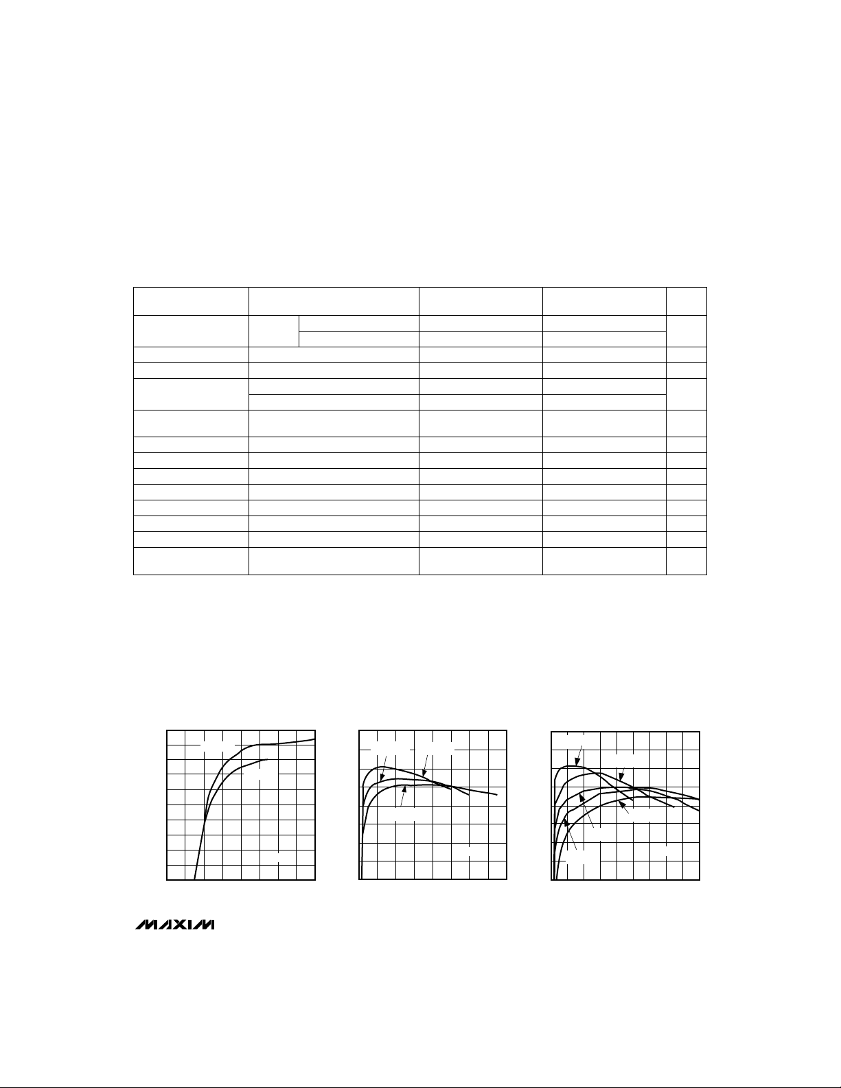
________________________________________________T ypical Operating Characteristics
(Circuit of Figure 3, TA = +25°C, V
MAXIMUM OUTPUT CURRENT
vs. SUPPLY VOLTAGE
1000
800
600
400
200
MAXIMUM OUTPUT CURRENT (mA)
0
MAX748A
MAX763A
0246810121416
SUPPLY VOLTAGE (V)
_________________________________________________________________________________________________
= 3.3V, unless otherwise noted.)
OUT
100
95
90
85
80
75
EFFICIENCY (%)
70
NOTE 2
65
60
0 100 200 300 400 500 600 700 800
EFFICIENCY vs. OUTPUT CURRENT
MAX763A
VIN = 7.0V
VIN = 5.0V
VIN = 11.0V
NOTE 2
OUTPUT CURRENT (mA)
EFFICIENCY vs. OUTPUT CURRENT
MAX748A
100
VIN = 4.5V
95
90
85
80
75
EFFICIENCY (%)
70
VIN = 12V
65
60
0 100 200 300 400 500 600 700 800 900
VIN = 6V
VIN = 16V
VIN = 9V
NOTE 2
OUTPUT CURRENT (mA)
3
Page 4
3.3V, Step-Down,
Current-Mode PWM DC-DC Converters
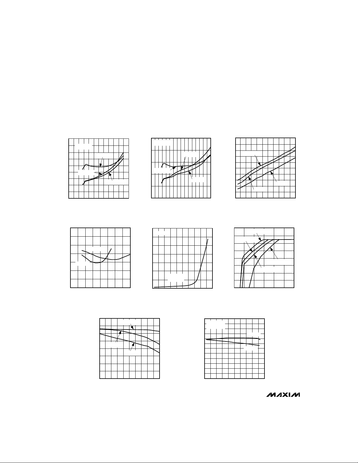
____________________________Typical Operating Characteristics (continued)
(Circuit of Figure 3, TA = +25°C, V
MAX763A
QUIESCENT SUPPLY CURRENT
vs. SUPPLY VOLTAGE
4.5
4.0
I
= 0mA
OUT
3.5
3.0
2.5
2.0
1.5
1.0
QUIESCENT SUPPLY CURRENT (mA)
0.5
0
MAX748A/MAX763A
0 1 2 3 4 5 6 7 8 9 10 11 12
275
250
225
200
175
MAX763A
150
OSCILLATOR FREQUENCY (kHz)
125
100
0 2 4 6 810121416
TA = +125°C
TA = -55°C
TA = +25°C
SUPPLY VOLTAGE (V)
OSCILLATOR FREQUENCY
vs. SUPPLY VOLTAGE
MAX748A
SUPPLY VOLTAGE (V)
= 3.3V, unless otherwise noted.)
OUT
QUIESCENT SUPPLY CURRENT
5.0
4.0
3.0
2.0
1.0
QUIESCENT SUPPLY CURRENT (mA)
3.5
3.0
2.5
2.0
1.5
1.0
SHUTDOWN CURRENT (µA)
0.5
vs. SUPPLY VOLTAGE
I
= OmA
OUT
TA = +125°C
0
0 2 4 6 8 10 12 14 16
NOTES 3, 4
0
-60 -40 -20 0 20 40 60 80 100 120 140
MAX748A
TA = -55°C
TA = +25°C
SUPPLY VOLTAGE (V)
SHUTDOWN CURRENT
vs. TEMPERATURE
I
= 0mA
OUT
V+ = 5V
TEMPERATURE (°C)
PEAK INDUCTOR CURRENT
vs. OUTPUT CURRENT
1000
800
600
400
200
PEAK INDUCTOR CURRENT (mA)
4.0
3.5
3.0
2.5
2.0
1.5
OUTPUT VOLTAGE (V)
1.0
0.5
VIN = 11V
VIN = 8V
0
0 50 100 150 200 250 300 350 400 450 500 550
OUTPUT CURRENT (mA)
OUTPUT VOLTAGE
vs. SUPPLY VOLTAGE
I
= 50mA
LOAD
I
= 200mA
LOAD
I
LOAD
I
= 300mA
LOAD
0
2.0 2.5 3.0 3.5 4.0 4.5 5.0
SUPPLY VOLTAGE (V)
VIN = 6V
= 500mA
OUTPUT VOLTAGE
4.0
3.5
3.0
2.5
2.0
1.5
OUTPUT VOLTAGE (V)
1.0
0.5
vs. OUTPUT CURRENT
VIN = 4.0V
VIN = 3.5V
VIN = 3.0V
0
0 50 100 150 200 250 300 350 400 450 500
OUTPUT CURRENT (mA)
OSCILATOR FREQUENCY (kHz)
OSCILLATOR FREQUENCY
vs. TEMPERATURE
300
I
= 100mA
OUT
V+ = 5V
250
200
150
100
50
0
-60 -40 -20 0 20 40 60 80 100 120 140
TEMPERATURE (°C)
MAX748A
MAX763A
4 _______________________________________________________________________________________
Page 5

3.3V, Step-Down,
Current-Mode PWM DC-DC Converters
_________________________________T ypical Operating Characteristics (continued)
(Circuit of Figure 3, TA = +25°C, V
SWITCHING WAVEFORMS,
CONTINUOUS CONDUCTION
2µs/div
A: SWITCH VOLTAGE (LX PIN), 5V/div, 0V TO +6V
B: INDUCTOR CURRENT, 200mA/div
C: OUTPUT VOLTAGE RIPPLE, 50mV/div
V+ = 6V, I
OUT
= 250mA
LINE-TRANSIENT RESPONSE
= 3.3V, unless otherwise noted.)
OUT
6V
0V
400mA
0mA
SWITCHING WAVEFORMS,
DISCONTINUOUS CONDUCTION
A
B B
C
2µs/div
A: SWITCH VOLTAGE (LX PIN), 5V/div, 0V TO +6V
B: INDUCTOR CURRENT, 100mA/div
C: OUTPUT VOLTAGE RIPPLE, 50mV/div
V+ = 6V, I
OUT
= 75mA
6V
0V
200mA
0mA
LOAD-TRANSIENT RESPONSE
A
C
MAX748A/MAX763A
10V
7V
0V
5ms/div
A: V
, 50mV/div
OUT
B: V+, 5V/div, 7.0V TO 10.0V
I
= 350mA
OUT
Note 2: Operation beyond the specifications listed in the
A
B
A: V
, 50mV/div
OUT
B: I
, 200mA/div, 0mA TO 500mA
OUT
V+ = 6V
Electrical Characteristics
5ms/div
may exceed the power dissipation ratings of
A
500mA
B
0mA
the device.
Note 3: Wide temperature range circuit of Figure 5 using Sprague surface-mount capacitors.
Note 4: Standby current includes all external component leakage currents. Capacitor leakage currents dominate at TA= +85°C.
_______________________________________________________________________________________
5
Page 6

3.3V, Step-Down,
Current-Mode PWM DC-DC Converters
_______________________________________________________________________Pin Description
PIN #
8-PIN DIP/SO
12
2 3 REF
37SS
48CC
5 9 OUT
6 10, 11 GND Ground*
MAX748A/MAX763A
7 12, 13, 14 LX Drain of internal P-channel power MOSFET*
8 1,15,16 V+ electrolytic capacitor in parallel. The 1µF capacitor must be as close
*16-pin wide SO package: All pins sharing the same name must be connected together externally.
16-PIN WIDE SO NAME FUNCTION
(MAX748A)
SHDN
4, 5, 6 N.C. No Connect—no internal connections to these pins.
Shutdown—active low. Connect to ground to power down chip; tie to V+ for normal
operation. Output voltage falls to 0V when
Reference Voltage Output (+1.23V) supplies up to 100µA for external loads.
Bypass to GND with a 0.047µF capacitor.
Soft-Start. Capacitor between SS and GND provides soft-start and
short-circuit protection.
Compensation Capacitor Input externally compensates the outer (voltage)
feedback loop. Connect to OUT with a 330pF capacitor.
Output-Voltage Sense Input provides regulation feedback sensing.
Connect to +3.3V output.
Supply Voltage Input. Bypass to GND with 1µF ceramic and large-value
to the GND and V+ pins as possible.*
SHDN
is low.
_________________Detailed Description
The MAX748A/MAX763A switch-mode regulators use a
current-mode pulse-width-modulation (PWM) control
system in a step-down (buck) regulator topography.
They convert an unregulated DC input voltage from 4V
to 11V (MAX763A) or from 4V to 16V (MAX748A) to a
regulated 3.3V output at 300mA. For loads less than
300mA, V+ may be less than 4.0V (see the Output
Voltage vs. Supply Voltage graph in the
Operating Characteristics
PWM architecture provides cycle-by-cycle current limiting, improved load-transient response, and simpler
outerloop design.
The controller consists of two feedback loops: an inner
(current) loop that monitors the switch current via the
current-sense resistor and amplifier, and an outer (voltage) loop that monitors the output voltage through the
error amplifier (Figure 1). The inner loop performs
cycle-by-cycle current limiting, truncating the power
transistor on-time when the switch current reaches a
predetermined threshold. This threshold is determined
by the outer loop. For example, a sagging output voltage produces an error signal that raises the threshold,
allowing the circuit to store and transfer more energy
during each cycle.
6 _______________________________________________________________________________________
). The current-mode
Typical
Figure 2 shows a capacitor connected to the soft-start
(SS) pin to ensure orderly power-up. A typical value is
0.047µF. SS controls both the SS timing and the maximum output current that can be delivered while maintaining regulation.
The charging capacitor slowly raises the clamp on the
error-amplifier output voltage, limiting surge currents
at power-up by slowly increasing the cycle-by-cycle
current-limit threshold. Table 1 lists timing characteristics for selected capacitor values and circuit conditions.
The overcurrent comparator trips when the load exceeds
approximately 1.2A. When either an undervoltage or overcurrent fault condition is detected, an SS cycle is actively
initiated, which triggers an internal transistor to discharge
the SS capacitor to ground. An SS cycle is also enabled
at power-up and when coming out of shutdown mode.
The overcurrent comparator triggers when the load
current exceeds approximately 1.2A. On each clock
cycle, the output FET turns on and attempts to deliver
current until cycle-by-cycle or overcurrent limits are
exceeded. Note that the SS capacitor must be greater
than 0.01µF for overcurrent protection to function properly. A typical value is 0.047µF.
Programmable Soft-Start
Overcurrent Limiting
Page 7

3.3V, Step-Down,
Current-Mode PWM DC-DC Converters
MAX748A/MAX763A
SHDN
SLOPE COMPENSATION
BIAS
GEN
Σ
PWM
COMPARATOR
SS CLAMP
330pF
1000pF
C5
C6
C1
0.047µF
OUT
CC
REF
SS
BANDGAP
1M
±35%
ERROR AMP
1.23V
GND
Figure 1. Detailed Block Diagram with External Components
FROM SHDN
SS CLAMP
SS
1M
C1
±35%
1.23V
MAX748A
MAX763A
OVERCURRENT COMPARATOR
RAMP
GEN
CURRENT
F/F
RQ
200kHz
OSC
SENSE AMP
S
Table 1. Typical Soft-Start Times
(Circuit of Figure 3, C4 = 150µF)
Circuit Cond. Soft-Start Time (ms) vs. C1 (µF)
V+ (V) I
12* 0 1 2 3 6
12* 200 7 17 20 80
12* 300 8 25 35 140
* MAX748A only
MAX748A 3.3V to 16.0V
MAX763A 3.3V to 11.0V
R
SENSE
V
IN
V+
LX
C2
1.0µF
22µH
D1
1N5817
C3
150µF
L1
V
OUT
3.3V
C4
150µF
MAX748A
MAX763A
UNDERVOLTAGE
LOCKOUT
V
UVLO
(mA) C1 = 0.01 C1 = 0.047 C1 = 0.1 C1 = 0.47
OUT
80 1 4 712
8 200 10 33 50 200
8 300 13 44 65 325
Figure 2. Soft-Start Circuitry Block Diagram
_______________________________________________________________________________________ 7
Page 8

3.3V, Step-Down,
Current-Mode PWM DC-DC Converters
Table 3. External Component Suppliers
Production Method Inductors Capacitors
Sumida Matsuo
CD105 series 267 series
Surface Mount Coiltronics Sprague
High Performance/ Sumida Sanyo
Miniature Through-Hole RCH895 series OS-CON series (very low ESR)
Through-Hole
Phone and FAX Numbers:
Coilcraft USA: (708) 639-6400, FAX: (708) 639-1469 Renco USA: (516) 586-5566, FAX: (516) 586-5562
Coiltronics USA: (305) 781-8900, FAX: (305) 782-4163 Sanyo USA: (0720) 70-1005, FAX: (0720) 70-1174
Matsuo USA: (714) 969-2491, FAX: (714) 960-6492 Sprague Elec. Co. USA: (603) 224-1961, FAX: (603) 224-1430
MAX748A/MAX763A
Nichicon USA: (708) 843-7500, FAX: (708) 843-2798
Japan: (06) 332-0871 Sumida USA: (708) 956-0666, FAX: (708) 956-0702
Japan: (03) 3607-5111, FAX: (03) 3607-5428
CTX series 595D/293D series
Coilcraft
DT series
Renco Nichicon
RL1284 series PL series (low ESR)
The undervoltage lockout feature monitors the supply
voltage at V+ and allows operation to start when V+
rises above 2.95V. When V+ falls, operation continues
until the supply voltage falls below 2.7V (typ). When an
undervoltage condition is detected, control logic turns
off the output power FET and discharges the SS capacitor to ground. This prevents partial turn-on of the power
MOSFET and avoids excessive power dissipation. The
control logic holds the output power FET off until the
supply voltage rises above approximately 2.95V, at
which time an SS cycle begins. When the input voltage
exceeds the undervoltage lockout threshold, switching
action will occur, but the output will not be regulated
until the input voltage exceeds 3.3V (no load). The
exact input voltage required for regulation depends on
load conditions (see the Output Voltage vs. Supply
Voltage graph in the
Typical Operating Characteristics
Shutdown Mode
The MAX748A/MAX763A are held in shutdown mode
Undervoltage Lockout
by keeping
output drops to 0V and the output power FET is held in
an off state. The internal reference also turns off, which
causes the SS capacitor to discharge. Typical supply
current in shutdown mode is 0.2µA. The actual design
limit for shutdown current is much less than the 100µA
specified in the
testing to tighter limits is prohibitive because the current takes several seconds to settle to a final value. For
8 _______________________________________________________________________________________
SHDN
at ground. In shutdown mode, the
Electrical Characteristics
. However,
normal operation, connect
shutdown mode initiates an SS cycle.
SHDN
to V+. Coming out of
Continuous-/Discontinuous-
Conduction Modes
The input voltage, output voltage, load current, and
inductor value determine whether the IC operates in
continuous or discontinuous mode. As the inductor
value or load current decreases, or the input voltage
increases, the MAX748A/MAX763A tend to operate in
discontinuous-conduction mode (DCM). In DCM, the
inductor current slope is steep enough so it decays to
zero before the end of the transistor off-time. In continuous-conduction mode (CCM), the inductor current
never decays to zero, which is typically more efficient
than DCM. CCM allows the MAX748A/MAX763A to
deliver maximum load current, and is also slightly less
).
noisy than DCM, because it doesn’t exhibit the ringing
that occurs when the inductor current reaches zero.
Internal Reference
The +1.23V bandgap reference supplies up to 100µA
at REF. A 1000pF bypass capacitor from REF to GND
is required.
The MAX748A/MAX763A’s internal oscillator is guaranteed to operate in the 159kHz to 212.5 kHz range over
temperature for V+ = 5V. Temperature stability over the
military temperature range is about 0.04%/°C.
Oscillator
Page 9

3.3V, Step-Down,
Current-Mode PWM DC-DC Converters
INPUT
MAX748A 3.3V TO 16.0V
MAX763A 3.3V TO 11.0V
1
3
C1
0.047µF
Figure 3. Standard 3.3V Step-Down Application Circuit Using Through-Hole Components (commercial temperture range)
SHDN
MAX748A
MAX763A
GND
62
V
IN
8
V+
LX
OUT
CCSS
REF
C6
1000pF
C2
1.0µF
C3
150µF
7
D1
L1
1N5817
22µH
5
C5
4
330pF
OUTPUT
3.3V
C4
150µF
OPTIONAL 21kHz LOWPASS OUTPUT FILTER
OUTPUT
L2
25µH
2.2µF
FILTER
OUTPUT
C7
MAX748A/MAX763A
Table 2. Component Table for
Wide Temperature Applications
C1(µF) C2(µF) C3(µF) C4(µF) C5(pF) C6(pF) L1(µH)
ThroughHole 0.047 1.0 150* 220* 330 1000 22
SO 0.047 1.0 68** 100*** 330 1000 22
* Sanyo OS-CON Series (very low ESR)
** 16V or greater maximum voltage rating.
*** 6.3V or greater maximum voltage rating.
____________Applications Information
Fixed +3.3V Step-Down
Figure 3 shows the standard 3.3V step-down circuit with
components shown for commercial temperature range
applications. Figures 4, 5, and Table 2 suggest external
component values for both SO and through-hole wide
temperature range applications. These circuits are useful in systems that require high current and high efficiency and are powered by an unregulated supply, such as
a battery or wall-plug AC-DC adapter.
The MAX748A delivers a guaranteed 300mA for input
voltages of 4V to 16V, and a guaranteed 500mA for
_______________________________________________________________________________________ 9
Converter Application
input voltages of 4.75V to 16V with 800mA typical output currents. The MAX763A delivers a guaranteed
300mA for input voltages of 4V to 11V, a guaranteed
500mA for input voltages of 4.75V to 11V, and has
700mA typical output currents. The MAX748A/
MAX763A operate from an input down to 3V (the upper
limit of undervoltage lockout), but with some reduction
in output voltage and maximum output current.
Inductor Selection
The MAX748A/MAX763A require no inductor design
because they are tested in-circuit, and are guaranteed
to deliver the power specified in the
Characteristics
with high efficiency using a single
Electrical
22µH inductor. The 22µH inductor’s incremental saturation current rating should be greater than 1A for
500mA load operation. Table 3 lists inductor types and
suppliers for various applications. The surface-mount
inductors have nearly equivalent efficiencies to the
larger through-hole inductors.
Output Filter Capacitor Selection
The primary criterion for selecting the output filter
capacitor is low effective series resistance (ESR). The
product of the inductor-current variation and the output
capacitor’s ESR determines the amplitude of the sawtooth ripple seen on the output voltage. Minimize the
output filter capacitor’s ESR to maintain AC stability.
Page 10

3.3V, Step-Down,
Current-Mode PWM DC-DC Converters
INPUT
MAX748A 3.3V TO 16.0V
MAX763A 3.3V TO 11.0V
1
SHDN
V
IN
8
V+
LX
C2
1.0µF
C3*
150µF
(16V)
7
D1
1N5817
MAX748A
MAX763A
3
C1
0.047µF
MAX748A/MAX763A
GND
62
5
OUT
4
CCSS
REF
C6
1000pF
*OS-CON Series (very low ESR)
C5
330pF
Figure 4. Standard 3.3V Step-Down Application Circuit Using
Through-Hole Components (all temperature ranges)
The capacitor’s ESR should be less than 0.25Ω to keep
the output ripple less than 50mV
p-p
over the entire current range (using a 22µH inductor). Capacitor ESR
usually rises at low temperatures, but OS-CON capacitors provide very low ESR below 0°C. Table 3 lists
capacitor suppliers.
Other Components
The catch diode should be a Schottky or high-speed
silicon rectifier with a peak current rating of at least
1.0A for full-load (500mA) operation. The 1N5817 is a
good choice. The 330pF outer-loop compensation
capacitor provides the widest input voltage range and
best transient characteristics.
Printed Circuit Layouts
A good layout is essential for stable, low-noise operation. The layouts and component placement diagrams
L1
22µH
OUTPUT
3.3V
C4*
220µF
(10V)
INPUT
MAX748A 3.3V TO 16.0V
MAX763A 3.3V TO 11.0V
1
SHDN
3
C1
0.047µF
GND
V
IN
8
V+
MAX748A
MAX763A
62
OUT
CCSS
REF
C6
1000pF
*Sprague 293D or 595D Series-16V. See Table 3
for alternative suppliers.
C2
1.0µF
C3*
68µF
(16V)
7
LX
D1
L1
1N5817
22µH
5
C5
330pF
4
OUTPUT
3.3V
C4*
100µF
(6.3V)
Figure 5. Standard 3.3V Step-Down Application Circuit Using
Surface-Mount Components (Commercial and Extended
Industrial Temperature Ranges)
in Figures 6-9 have been tested successfully over a
wide range of operating conditions. The 1µF input
bypass capacitor must be positioned as close to
the V+ and GND pins as possible. Also, place the
output capacitor as close to the OUT and GND pins as
possible. The traces connecting ground to the input
and output filter capacitors and to the catch diode
must be short to reduce inductance. Use an uninterrupted ground plane if possible.
Output-Ripple Filtering
A simple lowpass pi-filter (Figure 3) can be added to
the output to reduce output ripple to about 5mV
p-p
The cutoff frequency shown is 21kHz. Since the filter
inductor is in series with the circuit output, minimize the
filter inductor’s resistance so the voltage drop across it
is not excessive.
.
10 ______________________________________________________________________________________
Page 11

3.3V, Step-Down,
Current-Mode PWM DC-DC Converters
MAX748A/MAX763A
Figure 6. DIP PC Layout, Through-Hole Component Placement
Diagram (1X Scale)
Figure 8. DIP PC Layout, Solder Side (1X Scale) Figure 9. DIP PC Layout, Drill Guide (1X Scale)
Figure 7. DIP PC Layout, Component Side (1X Scale)
______________________________________________________________________________________ 11
Page 12

3.3V, Step-Down,
Current-Mode PWM DC-DC Converters
_____Pin Configurations (continued)
TOP VIEW
SHDN
REF
1
2
MAX748A
3
SS
MAX763A
4
CC
V+
8
LX
7
GND
6
OUT
5
SO
V+
1
SHDN
2
REF
3
MAX748A/MAX763A
N.C.
N.C.
N.C.
MAX748A
4
5
6
SS
7
CC
8
V+
16
V+
15
LX
14
LX
13
LX
12
GND
11
GND
10
OUT
9
Wide SO
_Ordering Information (continued)
____________________Chip Topographies
0.131"
3.327mm
SS
CC
OUT
GND
GND
TRANSISTOR COUNT: 298
SUBSTRATE CONNECTION: V+
SHDN
MAX748A
0.072"
1.829mm
V+
LXLX LX
V+ V+
REF
SHDN
V+
V+
V+
V+
0.116"
2.946mm
PART TEMP. RANGE PIN-PACKAGE
REF
MAX763ACPA 0°C to +70°C 8 Plastic DIP
MAX763ACSA 0°C to +70°C 8 SO
MAX763AC/D 0°C to +70°C Dice*
MAX763AEPA -40°C to +85°C 8 Plastic DIP
MAX763AESA -40°C to +85°C 8 SO
MAX763AMJA -55°C to +125°C 8 CERDIP
* Contact factory for dice specifications.
SS
OUTCC
MAX763A
TRANSISTOR COUNT: 281
SUBSTRATE CONNECTION: V+
12 ______________________________________________________________________________________
LX
LX
LX
0.116"
2.946mm
GND
 Loading...