Page 1
19-0197; Rev 1; 1/95
CCFL Backlight and
LCD Contrast Controllers
_______________General Description
The MAX753/MAX754 drive cold-cathode fluorescent
lamps (CCFLs) and provide the LCD backplane bias
(contrast) power for color or monochrome LCD panels.
These ICs are designed specifically for backlit notebook-computer applications.
Both the backplane bias and the CCFL supply can be
shut down independently. When both sections are shut
down, supply current drops to 25µA. The LCD contrast
and CCFL brightness can be adjusted by clocking separate digital inputs or using external potentiometers.
LCD contrast and backlight brightness settings are preserved in their respective counters while in shutdown.
On power-up, the LCD contrast counter and CCFL
brightness counter are set to one-half scale.
The ICs are powered from a regulated 5V supply. The
magnetics are connected directly to the battery, for
maximum power efficiency.
The CCFL driver uses a Royer-type resonant architecture. It can provide from 100mW to 6W of power to one
or two tubes. The MAX753 provides a negative LCD
bias voltage; the MAX754 provides a positive LCD bias
voltage.
________________________Applications
Notebook Computers
Palmtop Computers
Pen-Based Data Systems
Personal Digital Assistants
Portable Data-Collection Terminals
____________________________Features
♦ Drives Backplane and Backlight
♦ 4V to 30V Battery Voltage Range
♦ Low 500µA Supply Current
♦ Digital or Potentiometer Control of CCFL
Brightness and LCD Bias Voltage
♦ Negative LCD Contrast (MAX753)
♦ Positive LCD Contrast (MAX754)
♦ Independent Shutdown of Backlight and
Backplane Sections
♦ 25µA Shutdown Supply Current
______________Ordering Information
PART TEMP. RANGE
MAX753CPE
MAX753CSE 0°C to +70°C
MAX753C/D 0°C to +70°C Dice*
MAX753EPE -40°C to +85°C
MAX753ESE -40°C to +85°C 16 Narrow SO
MAX754CPE
MAX754CSE 0°C to +70°C
MAX754C/D 0°C to +70°C Dice*
MAX754EPE -40°C to +85°C
MAX754ESE -40°C to +85°C 16 Narrow SO
* Contact factory for dice specifications.
0°C to +70°C
0°C to +70°C
PIN-PACKAGE
16 Plastic DIP
16 Narrow SO
16 Plastic DIP
16 Plastic DIP
16 Narrow SO
16 Plastic DIP
MAX753/MAX754
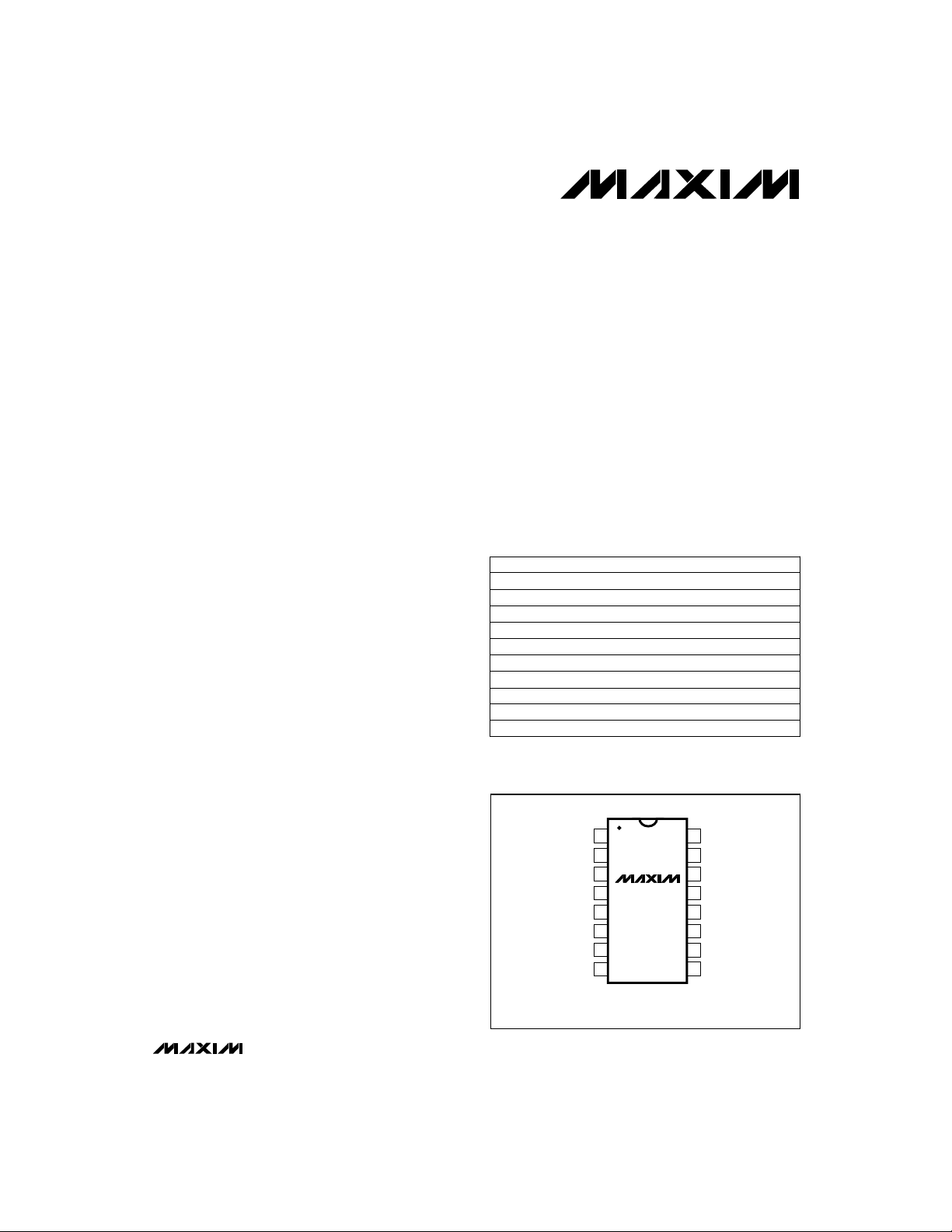
__________________Pin Configuration
TOP VIEW
V
DD
1
LADJ
2
LON
3
CON
CADJ
GND
REF
CFB
Block Diagram located at end of data sheet.
________________________________________________________________
MAX753
4
MAX754
5
6
7
8
DIP/SO
Maxim Integrated Products
Call toll free 1-800-998-8800 for free samples or literature.
LFB
16
BATT
15
LX
14
LDRV
13
PGND
12
CDRV
11
CS
10
CC
9
1
Page 2
CCFL Backlight and
LCD Contrast Controllers
ABSOLUTE MAXIMUM RATINGS
VDDto GND.................................................................-0.3V, +7V
PGND to GND.....................................................................±0.3V
BATT to GND.............................................................-0.3V, +36V
LX to GND............................................................................±50V
CS to GND.....................................................-0.6V, (V
Inputs/Outputs to GND (LADJ, CADJ, LON,
CON, REF, CFB, CC, CDRV, LDRV, LFB).....-0.3V, (V
Continuous Power Dissipation (T
Plastic DIP (derate 10.53mW/°C above +70°C) ...........842mW
Narrow SO (derate 8.70mW/°C above +70°C) .............696mW
Stresses beyond those listed under “Absolute Maximum Ratings” may cause permanent damage to the device. These are stress ratings only, and functional
operation of the device at these or any other conditions beyond those indicated in the operational sections of the specifications is not implied. Exposure to
absolute maximum rating conditions for extended periods may affect device reliability.
= +70°C)
A
DD
DD
+ 0.3V)
+ 0.3V)
ELECTRICAL CHARACTERISTICS
MAX753/MAX754
(VDD= 5V, BATT = 15V, CON = LON = 5V, LX = GND = PGND = 0V, I
= T
to T
T
A
MIN
SUPPLY AND REFERENCE
DIGITAL INPUTS AND DRIVER OUTPUTS
Driver On-Resistance
CCFT CONTROLLER
VCO Frequency
, unless otherwise noted.)
MAX
No external load
4V < VDD< 6V
0µA < IL< 100µA
LON = CON = CS = LFB = CFB =
LADJ = CADJ = 5V
LON = CON = CS = LFB = CFB = LADJ
= CADJ = LX = BATT = 0V (Note 1)
LON, CON, CADJ, LADJ; VDD= 4.5V
LON, CON, CADJ, LADJ; VDD= 5.5V
LON, CON, CADJ, LADJ; VIN= 0V or 5V
LDRV = CDRV = 2V
LDRV, CDRV;
VDD= 4.5V
VCS= 0V
Minimum, CFB = 5V
Maximum, CFB = 0V
Guaranteed monotonic
Operating Temperature Ranges
MAX75_C_ _ ........................................................0°C to +70°C
MAX75_E_ _......................................................-40°C to +85°C
Junction Temperature......................................................+150°C
Storage Temperature Range.............................-65°C to +160°C
Lead Temperature (soldering, 10sec).............................+300°C
= 0mA, all digital input levels are 0V or 5V,
REF
CONDITIONS
Output high
Output low
32 47
85 115
10
7
UNITSMIN TYP MAXPARAMETER
V430BATT Input Range
V4.5 5.5VDDSupply Range
V1.21 1.25 1.29REF Output Voltage
%/V0.1REF Line Regulation
mV515REF Load Regulation
mA0.5 2VDDQuiescent Current
µA25 40VDDShutdown Current
V0.8Input Low Voltage
V2.4Input High Voltage
µA±1Input Leakage Current
A0.5Driver Sink/Source Current
Ω
mV-10 20Zero-Crossing-Comparator Threshold Voltage (CS)
V1.2 1.3Overcurrent-Comparator Threshold Voltage (CS)
µA-5CS Input Bias Current
kHz
Bits5DAC Resolution
2 _______________________________________________________________________________________
Page 3
CCFL Backlight and
LCD Contrast Controllers
ELECTRICAL CHARACTERISTICS (continued)
(VDD= 5V, BATT = 15V, CON = LON = 5V, LX = GND = PGND = 0V, I
= T
to T
T
A
MIN
Feedback Voltage (CFB)
Feedback-Amplifier Output Current
LCD CONTROLLER
Switch On-Time
MAX753 Feedback Voltage (REF-LFB)
MAX754 Feedback Voltage (LFB)
TIMING (Note 2)
CADJ Low to CON Low or
LADJ Low to LON Low (t
Note 1: Maximum shutdown current occurs at BATT = LX = 0V.
Note 2: Timing specifications are guaranteed by design and not production tested.
, unless otherwise noted.)
MAX
)
SD
CONDITIONS
At full scale (DAC code = 31)
At preset DAC, CON = 0V, CADJ = 5V
(code = 15)
At zero scale (code = 0)
Source current, CFB = 0V, CC = 2.5V
Sink current, CFB = 5V, CC = 2.5V
BATT = 4V
BATT = 16V
BATT = 4V, LX = 0V
Guaranteed monotonic
At full scale (DAC code = 63)
At preset DAC, LON = 0V, LADJ = 5V
(code = 31)
At zero scale (code = 0)
At full scale (DAC code = 63)
At preset DAC, LON = 0V, LADJ = 5V
(code = 31)
At zero scale (code = 0)
LON = CON = CS = LFB = CFB = LADJ =
CADJ = LX = 0V
LON = CON = CS = LFB = CFB = LADJ =
CADJ = 0V, LX = BATT = 15V
REF
= 0mA, all digital input levels are 0V or 5V,
UNITSMIN TYP MAXPARAMETER
1210 1250 1290
745 782 820
320 343 365
50
200
25
0.5 1.5
1200 1240 1280
893 928 963
595 625 655
1210 1250 1290
905 938 971
610 635 660
mV
nA±100Feedback-Amplifier Input Bias Current
MHz1Feedback-Amplifier Unity-Gain Bandwidth
V/µs0.4Feedback-Amplifier Slew Rate
µA
µs
µs35 70Switching Period
Bits6DAC Resolution
mV
mV
nA±150LFB Input Leakage Current
µA12 20BATT Input Current
µA12 20LX Input Current
ns110Reset Pulse Width (tR)
ns0Reset Setup Time (tRS)
ns0Reset Hold Time (tRH)
ns100CADJ, LADJ High Width (tSH)
ns100CADJ, LADJ Low Width (tSL)
ns50
MAX753/MAX754
_______________________________________________________________________________________ 3
Page 4
CCFL Backlight and
LCD Contrast Controllers
______________________________________________________________Pin Description
PIN
1
MAX753/MAX754
DD
CS10
5V Power-Supply InputV
Digital Input for LCD Backplane Bias Adjustment. See Table 1.LADJ2
Digital Input to Control LCD Bias Section. See Table 1.LON3
Digital Input to Control CCFT Section. See Table 1.CON4
Digital Input for CCFT Brightness Adjustment. See Table 1.CADJ5
Analog GroundGND6
Reference Voltage Output, 1.25VREF7
Inverting Input for the CCFT Error AmplifierCFB8
Output of the CCFT Error AmplifierCC9
Connect to V
Leave unconnectedCDRV11
Power Ground Connection for LDRVPGND12
Gate-Driver Output. Drives LCD backplane N-channel MOSFET.LDRV13
LCD Backplane Inductor Voltage-Sense Pin. Used to sense inductor voltage for on time determination.LX14
Battery Connection. Used to sense battery voltage for on time determination.BATT15
Voltage Feedback for the LCD Backplane SectionLFB16
DD
_______________Theory of Operation
The MAX753/MAX754’s CCFL inverter is designed to
drive one or two cold-cathode fluorescent lamps
(CCFLs) with power levels from 100mW to 6W. These
lamps commonly provide backlighting for LCD panels
in portable computers.
Drive Requirements for CCFL Tubes
CCFL backlights require a high-voltage, adjustable AC
power source. The MAX753/MAX754 generate this AC
waveform with a self-oscillating, current-fed, parallel
resonant circuit, also known as a Royer-type oscillator.
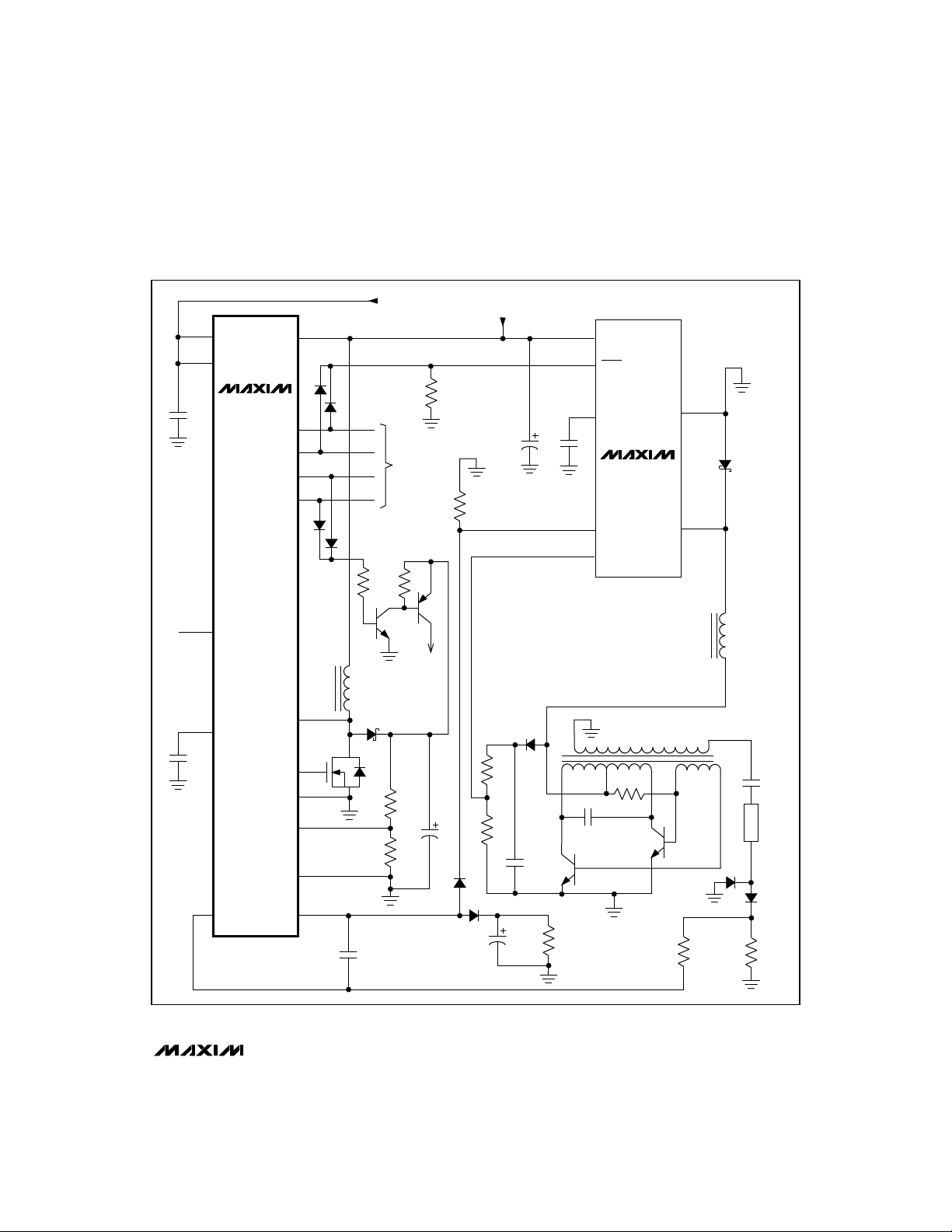
Figure 1 shows one such circuit. The Royer oscillator is
comprised of T1, C9, the load at the secondary, Q4,
and Q5. The circuit self-oscillates at a frequency determined by the effective primary inductance and capacitance. Q4 and Q5 are self-driven by the extra winding.
The current source feeding the Royer oscillator is comprised of L1, D5, and the MAX758A. When current from
the current source increases, so does the lamp current.
The lamp current is half-wave rectified by D7A and
CCFL Inverter
FUNCTIONNAME
D7B, and forms a voltage across resistor R8. The
MAX753’s error amplifier compares the average of this
voltage to the output of its internal DAC. Adjusting the
DAC output from zero scale to full scale (digital control)
causes the error amplifier to vary the tube current from
a minimum to a maximum. The DAC’s transfer function
is shown in Figure 2.
On power-up or after a reset, the counter sets the DAC
output to mid scale. Each rising edge of CADJ (with
CON high) decrements the DAC output. When decremented beyond full scale, the counter rolls over and
sets the DAC to the maximum value. In this way, a single pulse applied to CADJ decreases the DAC setpoint by one step, and 31 pulses increase the set-point
by one step.
The error amplifier’s output voltage controls the peak
current output of the MAX758A. The peak switch current is therefore controlled by the output of the error
amplifier. The lower the error amplifier’s output, the
lower the peak current. Since the current through the
current source is related to the current through the
tube, the lower the error amplifier’s output, the lower the
tube current.
4 _______________________________________________________________________________________
Page 5
CCFL Backlight and
LCD Contrast Controllers
MAX753/MAX754
+5V, ±5%
10
CS
1
V
DD
BATT
15
UNREGULATED INPUT VOLTAGE
1, 15, 16
V+
2
SHDN
D1B
CON
CADJ
LON
LADJ
LDRV
PGND
LFB
GND
D1A
4
5
3
2
D2B
D2A
L2
14
LX
13
12
16
6
9
CC
C1
MAX754CSE
11
CDRV
7
REF
C4
8
CFB
R16
3
C3C2
+5V CMOS
LOGIC
CONTROL
SIGNALS
R17
R2
R1
Q2
Q1
POSITIVE
CONTRAST
VOLTAGE
D3
Q3
R3
C6
R4
D6A
D6B
C5
D4
R5
R6
C8
Q4
C7
REF
MAX758ACWE
7
SS
8
CC
812
3,45
R10
C9
R7
GND
LX
T1
2
Q5
10, 11
D5
12, 13, 14
L1
61
CCFL
D7B
R18
C10
D7A
R8
Figure 1. CCFL and Positive LCD Power Supply
_______________________________________________________________________________________ 5
Page 6

CCFL Backlight and
LCD Contrast Controllers
1250
1221
1191
811
782
753
402
DAC OUTPUT VOLTAGE (mV)
372
343
MAX753/MAX754
01
2
3
ZERO SCALE
Figure 2. CCFT DAC Transfer Function
14 15 16 29 30 31
DAC CODE
MID SCALE FULL SCALE
MAX754
FULL-SCALE = 1.250V
HALF-SCALE = 0.782V
ZERO-SCALE = 0.343V
CON CADJ
LOGIC AND
5-BIT COUNTER
5-BIT VOLTAGE
OUTPUT DAC
In Figure 1, the MAX758A, L1, and D5 form a voltagecontrolled switch-mode current source. The current out
of L1 is proportional to the voltage applied to the SS
pin. The MAX758A contains a current-mode pulsewidth-modulating buck regulator that switches at
170kHz. The voltage on the SS pin sets the switch current limit and thus sets the current out of L1.
CCFL Current-Regulation Loop
Figure 3 shows a block diagram of the regulation loop,
which maintains a fixed CCFL average lamp current
despite changes in input voltage and lamp impedance.
This loop regulates the average value of the half-wave
rectified lamp current. The root mean square lamp current is related to, but not equal to, the average lamp
current. Assuming a sinusoidal lamp current, select R8
as follows:
where V
R
82=
= 1.25V and I
REF
V
π
REF
I
LAMP RMS
,
LAMP,RMS
is the desired full-
scale root mean square lamp current.
MAX758A
SS
SWITCH-MODE
VOLTAGE CONTROLLED
CURRENT SOURCE
I
BUCK
CENTER-TAP
ROYER
OSCILLATOR
TRANSISTOR
EMITTERS
C10
CCFL
R8
CFB
ERROR
AMPLIFIER
CC
C5
R18
Figure 3. CCFL Tube Current-Regulation Loop
6 _______________________________________________________________________________________
Page 7

CCFL Backlight and
LCD Contrast Controllers
MAX753/MAX754
V
(t)
V
TAP, PK
TAP
C10
V
(t)
SEC
(t)
V
LAMP
LAMP
LAMP,RMS
,
TAP
(t) =
.
T
pulse-frequency-modulation (PFM) switching regulator.
The MAX753 adds a simple diode-capacitor voltage
inverter to the switching regulator.
Constant-Current PFM Control Scheme
The LCD bias generators in these devices use a constant-peak-current PFM control scheme. Figure 6, which
shows the MAX754’s boost switching regulator, illustrates this control method. When Q3 closes (Q3 “on”) a
voltage equal to BATT is applied to the inductor, causing current to flow from the battery, through the inductor
and switch, and to ground. This current ramps up linearly, storing energy in the inductor’s magnetic field. When
Q3 opens, the inductor voltage reverses, and current
flows from the battery, through the inductor and diode,
and into the output capacitor. The devices regulate the
output voltage by varying how frequently the switch is
opened and closed.
The MAX753/MAX754 not only regulate the output voltage, but also maintain a constant peak inductor current, regardless of the battery voltage. The ICs vary the
switch on-time to produce the constant peak current,
and vary its off-time to ensure that the inductor current
reaches zero at the end of each cycle.
The internal circuitry senses both the output voltage
and the voltage at the LX node, and turns on the MOSFET only if: 1) The output voltage is out of regulation,
and 2) the voltage at LX is less than the battery voltage.
The first condition keeps the output in regulation, and
the second ensures that the inductor current always
resets to zero (i.e., the part always operates in discontinuous-conduction mode).
I
(t)
LAMP
Figure 4. Simple Model of the CCFL Figure 5. Voltage at the Center Tap of T1
The minimum operating input voltage is determined by
the transformer turns ratio (n), the lamp operating voltage (V
), and the ballast capactor (C10). Using a
LAMP
simple model of the CCFL (see Figure 4) we can calculate what the T1 center-tap voltage will be at maximum
lamp current. The voltage on the CCFL is in phase with
the current through it. Let us define I
√2I
LAMP,RMS
cos(ωt) and V
LAMP
(t) = √2V
cos(ωt); then the peak voltage at the center tap will be
as follows:
I
2
−
CV
10
I
LAMP RMS,,
nC
10ωφ()
,
LAMP RMS
,
LAMP RMS
sin
where,
V
TAP PK
φω=
tan
−
1
=−
n is the secondary-to-primary turns ratio of T1, and ω is
the frequency of Royer oscillation in radians per second. The voltage on the center tap of T1 is a full-wave
rectified sine wave (see Figure 5). The average voltage
at V
must equal the average voltage at the LX node
TAP
of the MAX758A, since there cannot be any DC voltage
on inductor L1; thus the minimum operating voltage
must be greater than the average voltage at V
LCD Bias Generators
The MAX753/MAX754’s LCD bias generators provide
adjustable output voltages for powering LCD displays.
The MAX753’s LCD converter generates a negative
output, while the MAX754’s generates a positive output.
The MAX753/MAX754 employ a constant-peak-current
t
_______________________________________________________________________________________ 7
Page 8

CCFL Backlight and
LCD Contrast Controllers
+5V INPUT
C1
0.22µF
2
3
LADJ
LON
CONTROL
MAX753/MAX754
MAX754
PGND
12
Figure 6. MAX754 Positive LCD-Bias Generator
V
DD
ON/OFF
PRESET
6-BIT COUNTER
CLK
6-BIT DAC
GND
6
1
ON-TIME
15
BATT
LOGIC
PULSE-SKIP
COMPARATOR
V
DAC
FULL-SCALE OUTPUT = 1.250V
HALF-SCALE OUTPUT = 0.938V
ZERO-SCALE OUTPUT = 0.635V
OFF-TIME
LOGIC
BATTERY
INPUT
L2
33µH
14
LX
LDRV
LFB
13
16
C2
10µF
D3
1N5819
Q3
R3
R4
POSITIVE
LCD-BIAS
OUTPUT
C6
10µF
35V
Table 1. CCFL Circuit Component Descriptions
ITEM DESCRIPTION
Integrating Capacitor. 1 / (C5 x R18) sets the dominant pole for the feedback loop, which regulates the lamp
C5
R18
R8
D7A, D7B
CCFL
8 _______________________________________________________________________________________
current. Set the dominant pole at least two decades below the Royer frequency to eliminate the AC component of the voltage on R8. For example, if your Royer is oscillating at 50kHz = 314159rad/s, you should set
1 / (C5 x R18) ≤ 3142rad/s.
Integrating Resistor. The output source-current capability of the CC pin (50µA) limits how small R18 can be.
Do not make R18 smaller than 70kΩ, otherwise CC will not be able to servo CFB to the DAC voltage (i.e., the
integrator will not be able to integrate) and the loop will not be able to regulate.
R8 converts the half-wave rectified lamp current into a voltage. The average voltage on R8 is not equal to the
root mean square voltage on R8. The accuracy of R8 is important since it, along with the MAX754 reference,
sets the full-scale lamp current. Use a ±1%-accurate resistor.
D7A and D7B half-wave rectify the CCFL lamp current. Half-wave rectification of the lamp current and then
averaging is a simple way to perform AC-to-DC conversion. D7A and D7B’s forward voltage drop and speed
are unimportant; they do not need to pass currents larger than about 10mA, and their reverse breakdown
voltage can be as low as 10V.
The circuit of Figure 1, with the components shown in the bill of materials (Table 4), will drive a 500V
ating cold-cathode fluorescent lamp at 6W of power with a +12V input voltage. The lower the input voltage,
the less power the circuit can deliver.
RMS
oper-
Page 9

CCFL Backlight and
LCD Contrast Controllers
Table 1. CCFL Circuit Component Descriptions (continued)
ITEM DESCRIPTION
The ballast capacitor linearizes the CCFL impedance and guarantees no DC current through the lamp. 15pF
C10
T1
C9
R10
R5, R6
D6B, C7, R7
D6A, R17
L1 Inductor for the Switching-Current Source. Use a 47µH to 150µH inductor with a 1A to 1.5A saturation current.
D5 Schottky Catch Diode. Use a 1A to 1.5A Schottky diode with low forward-voltage power.
C2 Supply Bypass Capacitor. Use low-ESR capacitor.
will work with just about any lamp. Depending on the lamp, you can try higher values, but this may cause the
regulation loop to become unstable. Larger values of C10 allow the circuit to operate with lower input voltages. Don’t forget that C10 must be a high-voltage capacitor and cannot be polarized. A lamp with a
1500V
T1 must have high primary inductance (greater than 30µH), otherwise an inflated value of C9 will be required
in order to keep the Royer frequency below 60kHz (the maximum allowed by most lamps). A higher T1 secondary-to-primary turns ratio allows lower-voltage operation, but increases the size of the transformer.
You must select a value for C9 high enough to keep the lamp current reasonably sinusoidal and yet low
enough that T1’s core does not saturate. For the Sumida EPS207 with a 171:1 turns ratio, choose a 0.22µF
value for C9. The characteristic impedance of the resonant tank equals , where L
netizing inductance of T1. The characteristic impedance is defined as the ratio of the voltage across the parallel LC circuit divided by the current flowing between the inductor and capacitor. This circulating current is
not delivered to the load. If C9 has too large a value, it will cause excessive circulating currents, which will in
turn saturate the core of T1. It’s easy to tell when you have excess circulating current in the resonant tank,
because when you touch T1 you burn your finger. However, reducing the value of C9 decreases tank Q,
which increases the harmonic content of the lamp-current waveform. If the lamp-current waveform does not
look sinusoidal, then the circuit may not regulate to the right root mean square current.
R10 sets the base current for Q4 and Q5. If you choose too large a value for R10, Q4 and Q5 will overheat.
Too small a value will waste base current and slightly degrade efficiency. The optimal value will depend on
how much power you are trying to deliver to the lamp. 510Ω is a good “always works but may not be the most
efficient” value for use with the FMMT619 transistors from ZETEX.
This resistive divider senses the voltage at the center tap of T1. When the CC pin on the MAX758A rises
above 1.25V, the internal switch turns off, interrupting power to the Royer oscillator and limiting the open-lamp
transformer center-tap voltage.
D6B, C7, and R7 form a soft-start clamp, which limits the rate-of-rise of the peak current in the MAX758A.
Make sure R7 is at least 100kΩ so it does not excessively load the CC pin.
D6A and R17 are also part of the soft-start clamp. The voltage on the SS pin controls the peak current in the
MAX758A’s switch. Make sure R17 is at least 100kΩ so it does not excessively load the CC pin.
maximum strike voltage will require C10 to withstand 1500 x √2= 2121V.
RMS
L
MAG
9
C
MAG
MAX753/MAX754
is the mag-
_______________________________________________________________________________________ 9
Page 10

CCFL Backlight and
LCD Contrast Controllers
Table 2. CCFL Circuit Design Example (Note 1)
PARAMETER SYMBOL MIN TYP MAX UNITS
CCFL Specifications
Strike Voltage (VS) V
Discharging Tube Current (IL) I
Discharging Tube Voltage (VL) V
LCD Contrast Voltage Specifications
Bias Voltage V
Output Current I
Royer Specifications
T1 Turns Ratio (Sec/Pri) (Note 2) n 171
T1 Resonating Inductance (Note 2) L
C9 Value (Note 3) C
MAX753/MAX754
C10 Value C
Royer Frequency w 317820.86 rad/s
MAX754 Specifications
Reference Voltage V
Second Volts Constant sV 0.000008 2.4E-05 sV
CCFL Circuit Calculations
R8 Current-Sensing Resistor R8 555.36037 Ω
Secondary Voltage Phase vs. Tube Voltage phi -1.1776341 Radian
T1 Center-Tap Peak Voltage V
Secondary Limit Voltage V
T1 Center-Tap Limit Peak Voltage 11.164844 V
R5/R6 R
LCD Circuit Calculations
V
Full-Load Switching Period T
IN(min)
L2 Inductance L2 1.96E-05 2.4E-05 H
L2 Peak Currrent 1.22704 A
R4/R3 R
Application Circuit Operating Range
Input Voltage V
Note 1: To perform your own calculations for the parameters given in Table 2 (Design Example), use the equations given in Table
Note 2: T1 = Sumida’s EPS207
Note 3: C9 = Wima’s SMD 7.3 __/63
3 (Design Equations).
S,RMS
LAMP,RMS
LAMP,RMS
LCD
LCD
MAG
RES
BAL
REF
TAP,PK
LIM
OTP,RATIO
FL
LCD,RATIO
IN
1100 1500 V
0.001376 0.005 A
435 V
16.3 32.6 V
0.0245 A
0.000045 H
2.2E-07 F
1.5E-11 F
1.25 V
9.3903817 V
1350 V
0.1341944 Ω/Ω
1.639E-06 s
0.0398724 Ω/Ω
5.978103 18 V
RMS
RMS
RMS
PEAK
RMS
PEAK
10 ______________________________________________________________________________________
Page 11

CCFL Backlight and
LCD Contrast Controllers
Table 3. Spreadsheet Design Equations
PARAMETER SYMBOL MIN TYP MAX
CCFL Specifications
Strike Voltage (VS) V
Discharging Tube Current (IL) I
Discharging Tube Voltage (VL) V
S,RMS
LAMP,RMS
LAMP,RMS
LCD Contrast Voltage Specifications
Bias Voltage V
Output Current I
LCD
LCD
Royer Specifications
T1 Turns Ratio (Sec/Pri) n 171
T1 Resonating Inductance L
C9 Value C
C10 Value C
MAG
RES
BAL
Royer Frequency w = SQRT [1 / (L
MAX754 Specifications
Reference Voltage V
REF
Second Volts Constant sV 0.000008 2.4E-05
CCFL Circuit Calculations
R8 Current-Sensing Resistor R8
Secondary Voltage Phase vs. Tube
Voltage
T1 Center-Tap Peak Voltage
Secondary Limit Voltage V
phi
V
TAP,PK
LIM
T1 Center-Tap Limit Peak Voltage = SQRT(2) * V
R5/R6 R
OTP,RATIO
LCD Circuit Calculations
V
Full-Load Switching Period T
IN(min)
FL
L2 Inductance L2 = L2(max) * 0.8
L2 Peak Currrent = sV(max) / L2(min)
R4/R3 R
LCD,RATIO
Application Circuit Operating Range
Input Voltage V
IN
1100 1500
= 0.28 *
I
LAMP,RMS(max)
435
= V
/ 2 32.6
LCD(max)
0.0245
0.000045
2.2E-07
1.5E-11
* C
RES
)]
MAG
1.25
= (2 / PI()) * V
TAP,PK
= PI() * V
(2 * I
= ATAN (-I
(C
BAL
= -SQRT(2) * I
(C
BAL
= V
= V
REF
= sV(min) / V
(V
= V
REF
* SQRT(2) /
REF
LAMP,RMS(max)
LAMP,RMS(max)
* w * + V
LAMP,RMS
LAMP,RMS(max)
* w * SIN(phi)) / n
S,RMS(max)
/ (D25 - 0.6 - V
IN(min)
- V
LCD(max)
/ (V
LCD(max)
)
* 0.9
/ n
LIM
REF
+ sV(min) /
)
IN(min)
- V
REF
)
0.005
/
)
/
= sV(min) ^ 2 / (2 * TFL*
V
LCD(max)
* I
)
18
LCD(min)
MAX753/MAX754
)
______________________________________________________________________________________ 11
Page 12

CCFL Backlight and
LCD Contrast Controllers
Table 4. Bill of Materials
RESISTOR VALUE (Ω) TOLERANCE (%)
R1 100,000 ±10
R2 100,000 ±10
R3 1,000,000 ±1
R4 40,200 ±1
R5 100,000 ±1
R6 13,300 ±1
R7 100,000 ±10
R8 549 ±1
R10 680 ±5
R16 100,000 ±10
R17 100,000 ±10
R18 100,000 ±5
MAX753/MAX754
CAPACITOR
C1 0.1 6
C2 22 20 Low ESR
C3 0.1 20
C4 0.1 6
C5 0.01 6 Non-polarized
C6 10 50
C7 1 6
C8 1 30
C9 22 63
C10 1.5E-5 3000 High voltage
VALUE (µF)
WORKING
VOLTAGE (V)
CHARACTERISTICS
OTHER
COMPONENTS
Q1 CMPTA06 SOT-23 80 MPSA06 Central Semi.
Q2 CMPT2907A SOT-23 60 2N2907 Central Semi.
Q3 SOT-23 60 3055EL Motorola
Q4
Q5 FMMT619 SOT-23 50 Zetex
D1A CMPD4150 SOT-23 75 1N4150 Central Semi.
D1B CMPD4150 SOT-23 75 1N4150 Central Semi.
D2A CMPD4150 SOT-23 75 1N4150 Central Semi.
D2B CMPD4150 SOT-23 75 1N4150 Central Semi.
D3 EC10QS05 D-64 50 1N5819 Nihon
D4 CMPD4150 SOT-23 75 1N4150 Central Semi.
D5 EC10QS02L D-64 20 1N5817 Nihon
D6A CMPD4150 SOT-23 75 1N4150 Central Semi.
D6B CMPD4150 SOT-23 75 1N4150 Central Semi.
D7A CMPD4150 SOT-23 75 1N4150 Central Semi.
D7B CMPD4150 SOT-23 75 1N4150 Central Semi.
Note: For T1, Use Sumida EPS207. Request No. USC-145, Special No. 6358-JP5-010.
12 ______________________________________________________________________________________
SURFACE-
MOUNT PART
NUMBER
MMFT3055ELT1
FMMT619
PACKAGE
SOT-23 50 Zetex
BREAKDOWN
VOLTAGE (V)
GENERIC
PART NO.
MANUFACTURER
Page 13

CCFL Backlight and
LCD Contrast Controllers
The voltage-regulation loop is comprised of resistors R3
Positive LCD Bias: MAX754
and R4, the pulse-skip comparator, the internal DAC,
the on-time and off-time logic, and the external power
components. The comparator compares a fraction of
the output voltage to the voltage generated by an onchip 6-bit DAC. The part regulates by keeping the voltage at LFB equal to the DAC’s output voltage. Thus,
you can set the output to different voltages by varying
the DAC’s output.
Varying the DAC output voltage (digital control) adjusts
the external voltage from 50% to 100% of full scale. On
power-up or after a reset, the counter sets the DAC output to mid scale. Each rising edge of LADJ (with LON
high) decrements the DAC output. When decremented
beyond zero scale, the counter rolls over and sets the
DAC to the maximum value. In this way, a single pulse
applied to LADJ decreases the DAC set point by one
step, and 63 pulses increase the set point by one step.
The MAX754’s DAC transfer function is shown in Figure 7.
The following equation relates the switching regulator’s
regulated output voltage to the DAC’s voltage:
VV1
OUT DAC
=+
R3
R4
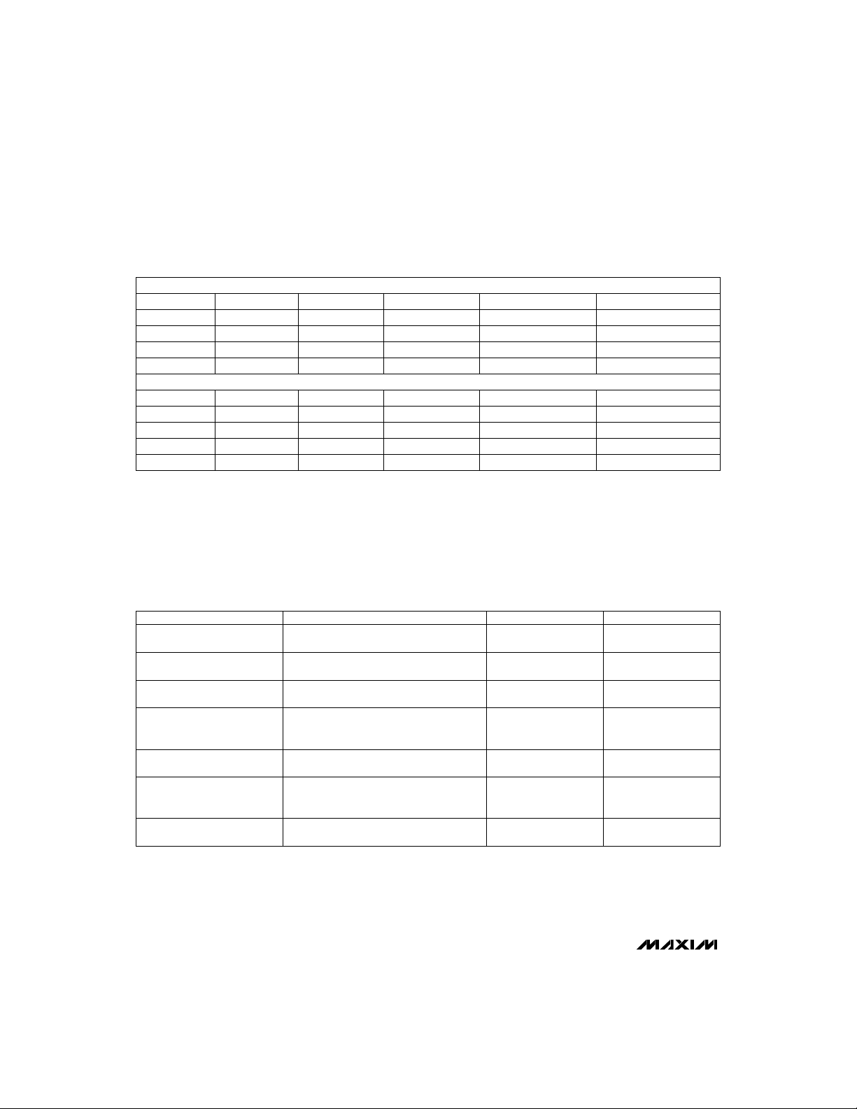
Table 5 is the logic table for the LADJ and LON inputs,
which control the internal DAC and counter. As long as the
timing specifications for LADJ and LON are observed, any
sequence of operations can be implemented.
Negative LCD Bias: MAX753
The LCD bias generator of the MAX753 (Figure 8) generates its negative output by combining the switching
regulator of the MAX754 with a simple diode-capacitor
voltage inverter. To best understand the circuit, look at
the part in a steady-state condition. Assume, for
instance, that the output is being regulated to -30V, and
that the battery voltage is +10V. When Q3 turns on, two
things occur: current ramps up in the inductor, just like
with the boost converter; and the charge on C15 (transferred from the inductor on the previous cycle) is transferred to C6, boosting the negative output. At the end of
the cycle, the voltage on C15 is 30V + Vd, where Vd is
the forward voltage drop of Schottky diode D3, and 30V
is the magnitude of the output.
When the MOSFET turns off, the inductor’s energy is
transferred to capacitor C15, charging the capacitor to
a positive voltage (V
) that is higher than |V
HIGH
OUT
|. In
this instance, diode D8 allows current to flow from the
right-hand side of the flying capacitor (C15) to ground.
When the MOSFET turns on, the left-hand side of
capacitor C15 is clamped to ground, forcing the right-
1250
1240
1230
947
938
928
655
DAC OUTPUT VOLTAGE (mV)
645
635
01
2
ZERO SCALE
Figure 7. MAX754 LCD DAC Transfer Function
hand side to -V
HIGH
30 31 32 61 62 63
DAC CODE
MID SCALE FULL SCALE
. This voltage is more negative than
the output, forcing D3 to conduct, and transferring
charge from the flying capacitor C15 to the output
capacitor C6. This charge transfer happens quickly,
resulting in a voltage spike at the output due to the
product of the output capacitor’s equivalent series
resistance (ESR) and the current that flows from C15 to
C6. To limit this drop, resistor R19 has been placed in
series with D3. R19 limits the rate of current flow. At the
end of this cycle, the flying capacitor has been discharged to 30V + Vd.
If BATT(MAX) (i.e., either the fully charged battery voltage, or the wall-cube voltage) is greater than
|V
(MIN)|, tie the cathode of D8 to BATT instead of
OUT
GND, as shown by the dashed lines in Figure 8.
Efficiency is lower with this method, so tie the cathode
of D8 to GND whenever possible.
The MAX753’s regulation loop is similar to that of the
MAX754. The MAX753, however, uses different power
components, and its feedback resistors are returned to
the reference (1.25V) rather than ground.
The MAX753’s PFM comparator compares a fraction of
the output voltage to the voltage generated by the onchip 6-bit DAC. The part regulates by keeping the voltage at LFB equal to the DAC’s output voltage. Thus,
you can set the LCD bias voltage to different voltages
by varying the DAC’s output.
MAX753/MAX754
______________________________________________________________________________________ 13
Page 14
CCFL Backlight and
LCD Contrast Controllers
Table 5. Logic-Signal Truth Table
CCF CONTROL
LON LADJ CON CADJ CCFT STATUS
X X 0 0 Off
X X 0 1 On
X X 1 0 On
X X 1
LCD BIAS CONTROL
LON LADJ CON CADJ LCD STATUS
0 0 X X Off
0 1 X X On
MAX753/MAX754
1 0 X X On
1
0→1
X X On
Hold = maintain last DAC value in counter
Reset = set DAC counter to half scale
Dec = decrement DAC counter one step
Off = section turned off, sleep state
On = section turned on
X = don’t care
Table 6. Component Suppliers
MANUFACTURER
Central Semiconductor
Coiltronics
Maxim
Nihon (NIEC)*
Sumida
Wima
Zetex (516) 543-7100 (516) 864-7630
* Contact John D. Deith, ask for “Maxim Discount” on orders less than 5k units.
145 Adams Ave.
Hauppauge, NY 11788
6000 Park of Commerce Blvd.
Boca Raton, FL 33287
120 San Gabriel Dr.
Sunnyvale, CA 94025
c/o Quantum Marketing
12900 Rolling Oaks Rd.
Twin Oaks, CA 93518
5999 New Wilke Rd., Suite 110
Rolling Meadows, IL 60008
2269 Saw Mill River Rd., Suite 400
P.O. Box 217
Elmsford, NY 10523
87 Modular Ave.
Commack, NY 11725
ADDRESS PHONE FAX
0→1
On
(516) 435-1110 (516) 435-1824
(407) 241-7876 (407) 241-9339
(408) 737-7600 (408) 737-7194
(805) 867-2555 (805) 867-2698
(708) 956-0666 (708) 956-0702
(914) 347-2474 (914) 347-7230
CCFT DAC
Hold
Reset
Hold
Dec
LCD DAC
Hold
Reset
Hold
Dec
14 ______________________________________________________________________________________
Page 15

+5V INPUT
C1
0.22µF
2
LADJ
CONTROL
MAX753
PGND
3
LON
12
V
DD
ON/OFF
PRESET
6-BIT COUNTER
CLK
6-BIT DAC
GND
6
1
15
ON-TIME
LOGIC
BATT
V
DAC
PULSE-SKIP
COMPARATOR
Figure 8. MAX753 Negative LCD-Bias Generator
1240
1230
1220
937
928
918
645
DAC OUTPUT VOLTAGE (mV)*
635
625
14
LX
OFF-TIME
LOGIC
CCFL Backlight and
LCD Contrast Controllers
BATTERY
INPUT
L2
33µH
C15
1µF
LDRV
13
Q3
LFB
16
7
REF
C4
0.22µF
The MAX753’s DAC transfer function is shown in Figure 9.
The following equation relates the switching regulator’s
regulated output voltage to the DAC’s voltage (REF - LFB):
V REF 1
OUT
The value REF - LFB (and not LFB) is specified in the
Electrical Characteristics
voltage occurs for the largest value of REF - LFB.
The MAX753’s combination boost converter and
charge-pump inverter was chosen over a conventional
buck-boost inverter because it allows the use of lowcost N-channel MOSFETs instead of more expensive Pchannel ones. Additionally, its efficiency is 5% to 10%
better than a standard buck-boost inverter.
ALTERNATE
D8 CONNECTION
(SEE TEXT)
C2
10µF
R19
2.2Ω
D8
1N5819
=−+
. The most negative output
D3
1N5819
R3
R4
NEGATIVE
LCD-BIAS
OUTPUT
C6
10µF
35V
V
DD
R3
REF LFB
−
()
R4
MAX753/MAX754
01
2
ZERO SCALE
* DAC OUTPUT VOLTAGE = REF - LFB
30 31 32 61 62 63
DAC CODE
MID SCALE FULL SCALE
Figure 9. MAX753 LCD DAC Transfer Function
______________________________________________________________________________________ 15
Page 16

CCFL Backlight and
LCD Contrast Controllers
_____________________Block Diagram
LADJ LON BATT LX
MAX753/MAX754
32
CONTROL
PRESETCLK
6-BIT
COUNTER
6-BIT
D/A CONVERTER
ON-TIME
LOGIC
MAX753/MAX754
5-BIT
D/A CONVERTER
5-BIT
COUNTER
PRESETCLK
LOGIC
CONTROL
CON CADJ
45
12 6
OFF-TIME
PULSE-SKIP
COMPARATOR
AMPLIFIER
PGND GND
1415
LOGIC
ERROR
LDRV
LFB
V
CDRV
CFB
REF
REF
___________________Chip Topography
V
13
16
1
DD
7
11
8
9
CC
10
CS
LADJ
LON
CON
CADJ
GND
REF
TRANSISTOR COUNT: 321;
SUBSTRATE CONNECTED TO VDD.
DD
LFB
CFB
0.076"
(1.930mm)
CC
BATT
CS
LX
LDRV
PGND
CDRV
0.112"
(2.845mm)
Maxim cannot assume responsibility for use of any circuitry other than circuitry entirely embodied in a Maxim product. No circuit patent licenses are
implied. Maxim reserves the right to change the circuitry and specifications without notice at any time.
16
__________________Maxim Integrated Products, 120 San Gabriel Drive, Sunnyvale, CA 94086 (408) 737-7600
© 1995 Maxim Integrated Products Printed USA is a registered trademark of Maxim Integrated Products.
 Loading...