

Page 1
MAX7472/MAX7473
HDTV Anti-Aliasing Filters with Triple-Input Mux
________________________________________________________________
Maxim Integrated Products
1
Ordering Information
19-0619; Rev 0; 8/06
For pricing, delivery, and ordering information, please contact Maxim/Dallas Direct! at
1-888-629-4642, or visit Maxim’s website at www.maxim-ic.com.
Continuously Variable Anti-Aliasing Filter
5MHz to 34MHz in 256 Steps
3:1 Input Mux on Each Video Filter
Supports All Standard Video and Computer Input
Formats
480i, 480p, 720p, 1080i
QVGA, VGA, SVGA, XGA, SXGA, UXGA
Y PB PR, GsBR, RGBHV, Y/C, CVBS
Accepts Any Input Sync Format
Sync on Y, Sync on G, External Sync
(Positive or Negative)
Sync on All Channels
Buffered Outputs Drive Standard 150Ω Video Load
0dB (MAX7472)
+6dB (MAX7473)
DC- or AC-Coupled Outputs
Single +5V Analog and +3.3V Digital Supplies
5mW Power-Down Mode
Lead (Pb)-Free 28-Pin TQFN Package
General Description
The MAX7472/MAX7473 triple-channel anti-aliasing filters and buffers with triple-input mux are ideal for highdefinition (HD) and standard-definition (SD) television
(TV) applications. Compatible with 1080i, 720p, 480p,
and 480i scanning system standards as well as computer format signals, the MAX7472/MAX7473 support
component video (Y PBPR, GsBR, and RGBHV) as well
as composite (CVBS) and S-video (Y/C).
The MAX7472/MAX7473 limit the input bandwidth for
anti-aliasing and out-of-band noise reduction prior to
digital conversion by an ADC or video decoder. The
frequency response of the MAX7472/MAX7473 can be
continuously varied in 256 linear steps from below SD
response to beyond HD response through an I2C interface. The adjustable cutoff frequency allows filter optimization for sampling rate and noise reduction. The
MAX7472/MAX7473 also include 3:1 multiplexers for
selection of three complete sets of video inputs through
the I2C interface.
The MAX7472/MAX7473 drive a 2V
P-P
video signal into
a standard 150Ω load. The inputs are AC-coupled and
the outputs can be either DC- or AC-coupled. The
MAX7472 has a gain of 0dB and the MAX7473 has a
gain of +6dB. Both devices are available in a 28-pin
TQFN package and are fully specified over the uppercommercial (0°C to +85°C) temperature range.
Features
EVALUATION KIT
AVAILABLE
Note: All devices are specified over the 0°C to +85°C operat-
ing temperature range.
+Indicates lead-free packaging.
*EP = Exposed pad.
**
Future product—contact factory for availability.
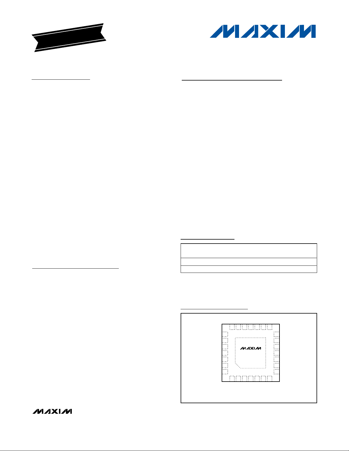
Pin Configuration
HDTV (LCD, PDP, DLP, CRT)
Set-Top Boxes
Personal Video Recorders
Home Theaters
Applications
Typical Operating Circuit appears at end of data sheet.
PART PIN-PACKAGE PKG CODE
MAX7472UTI+ 28 TQFN-EP* T2855-8 0
MAX7473UTI+** 28 TQFN-EP* T2855-8 +6
BUFFER
GAIN (dB)
TOP VIEW
AGND
AGND
AV
INA1
INB1
22
DD
A0
23
24
A1
25
26
27
28
DDAVDD
OUT1
AV
2021 19 17 16 15
+
12
INC1
AGND
5mm x 5mm
*EXPOSED PAD.
OUT3
OUT2
18
MAX7472
MAX7473
4567
3
INA2
INB2
INC2
TQFN
EP*
DVDDSDA
INA3
AGND
14
SCL
SYNCC
13
12
SYNCB
SYNCA
11
10
DGND
INC3
9
8
INB3
Page 2
MAX7472/MAX7473
HDTV Anti-Aliasing Filters with Triple-Input Mux
2 _______________________________________________________________________________________
ABSOLUTE MAXIMUM RATINGS
ELECTRICAL CHARACTERISTICS
(AVDD= +5V ±5%, DVDD= 2.7V to 3.6V, R
LOAD
= 150Ω to AGND, CIN= 0.1µF, TA= 0°C to +85°C, unless otherwise noted. Typical
values are at T
A
= +25°C.)
Stresses beyond those listed under “Absolute Maximum Ratings” may cause permanent damage to the device. These are stress ratings only, and functional
operation of the device at these or any other conditions beyond those indicated in the operational sections of the specifications is not implied. Exposure to
absolute maximum rating conditions for extended periods may affect device reliability.
AVDDto AGND .........................................................-0.3V to +6V
DV
DD
to DGND.........................................................-0.3V to +4V
AGND to DGND.....................................................-0.3V to +0.3V
INA_, INB_, INC_ to AGND...........................................................
............................-0.3V to the lower of (AV
DD
+ 0.3V) and +6V
OUT_ to AGND.…..-0.3V to the lower of (AV
DD
+ 0.3V) and +6V
SYNC_, A_ to AGND.....................................................................
...............................-0.3V to the lower of (AV
DD
+ 0.3V) and +6V
SCL, SDA to DGND .................................................-0.3V to + 6V
Maximum Current into Any Pin
(except AV
DD
, DVDD, and OUT) ...................................±50mA
Continuous Power Dissipation (T
A
= +70°C)
28-Pin TQFN (derate 34.5mW/°C above +70°C) ........2758mW
Operating Temperature Range.............................. 0°C to +85°C
Storage Temperature Range ............................-65°C to +150°C
Junction Temperature......................................................+150°C
Lead Temperature (soldering, 10s) .................................+300°C
)
PARAMETER SYMBOL CONDITIONS MIN TYP MAX UNITS
Filter Passband Response A
Filter Stopband Attenuation A
Group-Delay Deviation Δt
Group-Delay Matching t
Bypass Frequency Response
SD Differential Gain dG 5-step modulated staircase (Note 2) 0.25 %
SD Differential Phase dφ 5-step modulated staircase (Note 2) 0.25 D egr ees
Signal-to-Noise Ratio SNR
SD Line-Time Distortion H
SD Field-Time Distortion V
G(MATCH
HD: f = 100kHz to 30MHz, relative to 100kHz
(Note 1)
PB
SD: f = 100kHz to 5.75MHz, relative to
100kHz (Note 2)
HD: f = 74MHz (Note 1) 57
SB
SD: f = 27MHz (Note 2) 63
HD: 100kHz to 30MHz, relative to 100kHz
(Note 1)
G
SD: 100kHz to 5.75MHz, relative to 100kHz
(Note 2)
HD: channel to channel, 100kHz to 2MHz
(Note 1)
SD: channel to channel, 100kHz to 500kHz
(Note 2)
-3dB, bypass mode, independent of filter
setting
Output signal (2V
to 30MHz) (Note 1)
DIST
DIST
Deviations in a line with an 18µs, 100 IRE bar,
1 line = 63.5µs (Note 2)
Deviations in 130 lines with 18µs, 100 IRE
bars (Note 2)
) to RMS noise (100kHz
P-P
-3 -0.6 +1
±0.1 ±1.0
20
15
5
1.5
100 MHz
69 dB
0.3 %
0.3 %
dB
dB
ns
ns
Page 3
MAX7472/MAX7473
HDTV Anti-Aliasing Filters with Triple-Input Mux
_______________________________________________________________________________________ 3
ELECTRICAL CHARACTERISTICS (continued)
(AVDD= +5V ±5%, DVDD= 2.7V to 3.6V, R
LOAD
= 150Ω to AGND, CIN= 0.1µF, TA= 0°C to +85°C, unless otherwise noted. Typical
values are at T
A
= +25°C.)
PARAMETER SYMBOL CONDITIONS MIN TYP MAX UNITS
Clamp Settling Time
Minimum Functional Input Sync
Amplitude
Low-Frequency Gain
Low-Frequency Gain Matching 100kHz 0.05 dB
Maximum Input Voltage
Amplitude
Maximum Output Voltage
Amplitude
Output Clamping Level Variation (Notes 1, 4) ±120 mV
Mux Crosstalk -80 dB
Channel-to-Channel Isolation 62 dB
Power-Supply Rejection Ratio PSRR 50 dB
DIGITAL INPUTS (A1, A0, SYNC_)
Input Logic High Voltage V
Input Logic Low Voltage V
Input Leakage Current I
Input Capacitance C
DIGITAL INPUTS (SDA, SCL)
Input Logic High Voltage V
Input Logic Low Voltage V
Input Hysteresis V
Input Leakage Current I
Input Capacitance C
DIGITAL OUTPUT (SDA)
Output Logic Low Voltage V
Tri-State Leakage Current I
Tri-State Output Capacitance C
POWER REQUIREMENTS
Analog Supply Voltage Range AV
Digital Supply Voltage Range DV
Analog Supply Current I
Digital Supply Current I
To 1% with 100 IRE step
(Note 3)
Positive 350
Negative 650
125 mV
TA = +25°C, MAX7472 (Note 1) -0.5 0 +0.5
= +25°C, MAX7473 (Note 1) 5.5 6 6.5
T
A
MAX7472 2.4
MAX7473 1.2
DC to 30MHz 2.4 V
IH
IL
IN
IN
IH
IL
HYST
IN
IN
OL
L
OUT
DD
DD
AVDD
DVDD
VIN = 0 to DV
VIN = 0 to DV
I
= 3mA 0.4 V
SINK
VIN = 0 to DV
DD
DD
DD
Normal operation, no load 180 200
Power-down mode, no load 1 1.5
2.0 V
±1 ±10 µA
6pF
0.7 x DV
DD
0.3 x DV
0.05 x DV
DD
±0.1 ±10 µA
6pF
±0.1 ±10 µA
6pF
4.75 5 5.25 V
2.7 3.3 3.6 V
25 µA
0.8 V
DD
H
dB
V
P-P
P-P
V
V
V
mA
Page 4
MAX7472/MAX7473
HDTV Anti-Aliasing Filters with Triple-Input Mux
4 _______________________________________________________________________________________
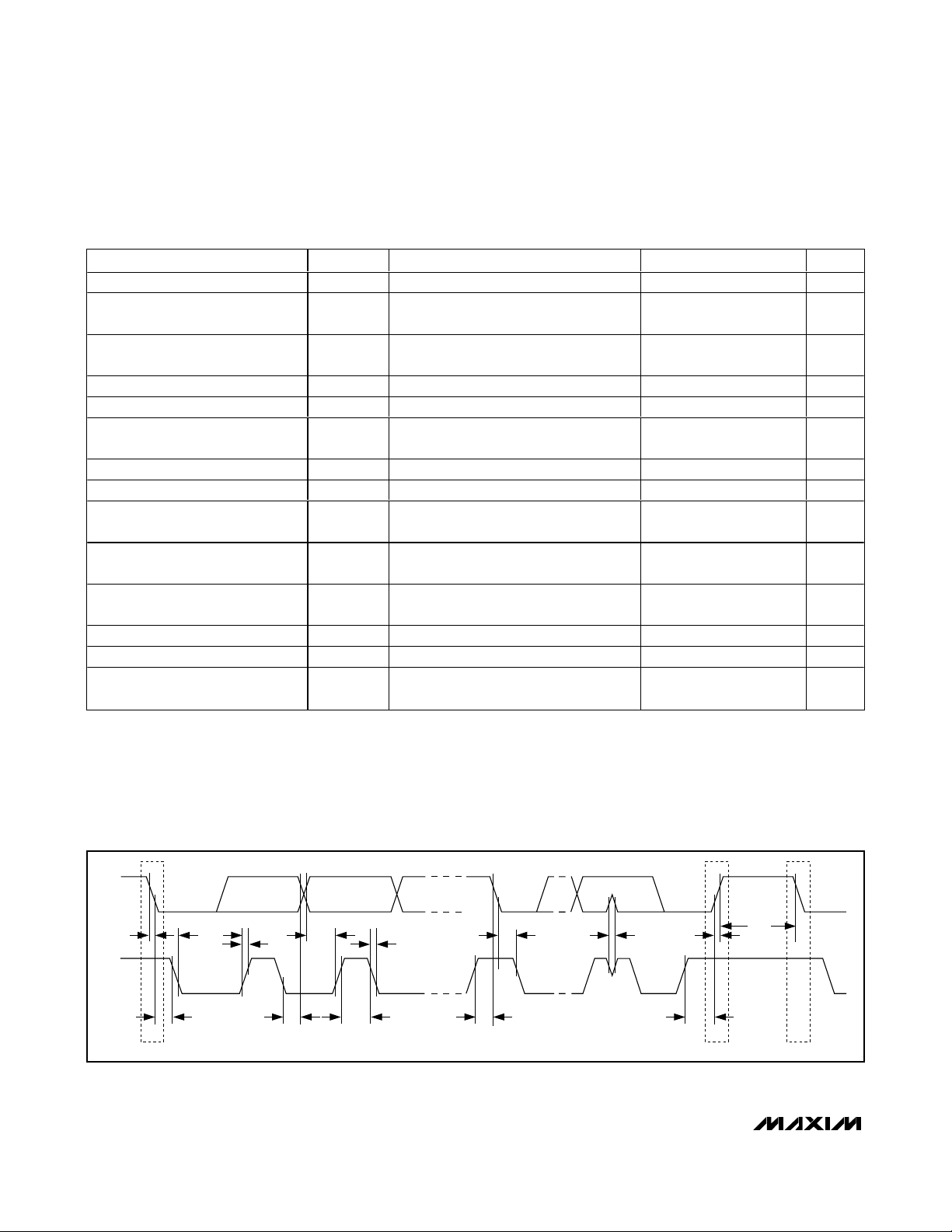
TIMING CHARACTERISTICS
(AVDD= +5V ±5%, DVDD= 2.7V to 3.6V, TA= 0°C to +85°C, unless otherwise noted. Typical values are at TA= +25°C.) (Figure 1)
Note 1: The filter passband edge is set to code 255.
Note 2: The filter passband edge is set to code 40.
Note 3: 1H is the total line period, depending on the video standard. For NTSC, this is 63.5µs, for HDTV, the line period is 29.64µs.
Note 4: The clamp level is at the sync tip for signals with sync pulses, and is at the blanking level otherwise.
Note 5: A master device must provide a hold time of at least 300ns for the SDA signal (referred to V
IL
of the SCL signal) to bridge
the undefined region of SCL’s falling edge.
Note 6: C
b
= total capacitance of one bus line in pF. tRand tFmeasured between 0.3VDDand 0.7VDD.
Note 7: Input filters on the SDA and SCL inputs suppress noise spikes less than 50ns.
Figure 1. 2-Wire Serial-Interface Timing Diagram
Serial Clock Frequency f
Bus Free Time Between STOP (P)
and START (S) Conditions
Hold Time (Repeated) START (Sr)
Condition
SCL Pulse-Width Low t
SCL Pulse-Width High t
Setup Time for a Repeated START
(Sr) Condition
Data Hold Time t
Data Setup Time t
Rise Time of Both SDA and SCL
Signals, Receiving
Fall Time of Both SDA and SCL
Signals, Receiving
Fall Time of SDA Signal,
Transmitting
Setup Time for STOP (P) Condition t
Capacitive Load for Each Bus Line C
Pulse Width of Spikes Suppressed
by the Input Filter
PARAMETER SYMBOL CONDITIONS MIN TYP MAX UNITS
SCL
t
BUF
t
HD;STA
LOW
HIGH
t
SU;STA
HD;DAT
SU;DAT
t
r
t
f
t
f
SU;STO
b
t
SP
After this period, the first clock pulse is
generated
(Note 5) 0 0.9 µs
(Note 6)
(Note 7) 0 50 ns
0 400 kHz
1.3 µs
0.6 µs
1.3 µs
0.6 µs
0.6 µs
100 ns
0 300 ns
0 300 ns
20 +
0.1C
b
0.6 µs
300 ns
400 pF
SDA
t
BUF
t
r
PS
SCL
t
f
S
t
t
HD;STA
LOW
t
HD;DAT
t
SU;DAT
t
r
t
HIGH
t
f
t
SU;STA
Sr
t
HD;STA
t
SP
t
SU;STO
Page 5
MAX7472/MAX7473
HDTV Anti-Aliasing Filters with Triple-Input Mux
_______________________________________________________________________________________
5
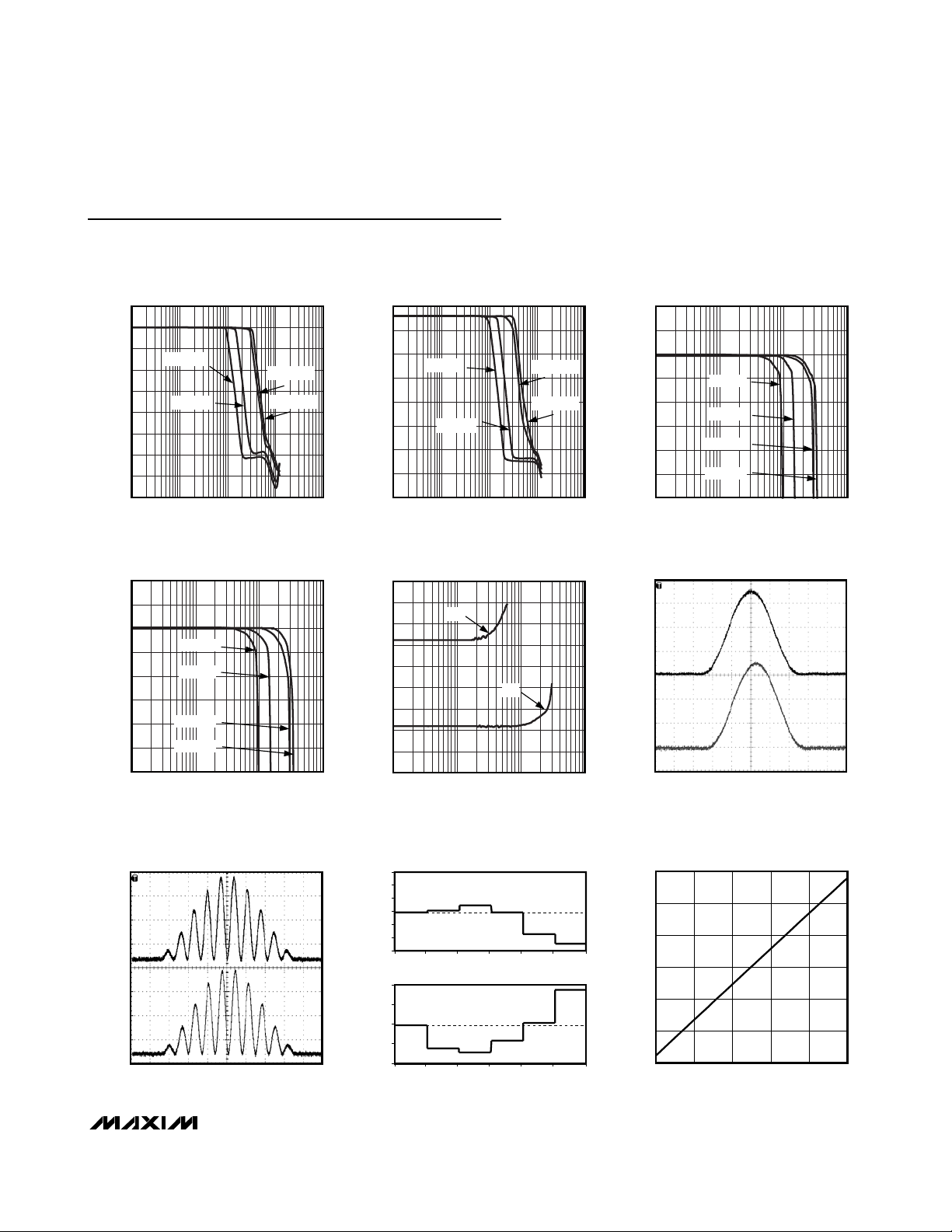
Typical Operating Characteristics
(AVDD= +5V, DVDD= 3.3V, R
LOAD
= 150Ω to GND, CIN= 0.1µF, TA= +25°C.)
FREQUENCY RESPONSE (MAX7472)
10
0
-10
-20
-30
-40
RESPONSE (dB)
-50
-60
-70
-80
CODE 40
CODE 90
0.1 101 100 1000
FREQUENCY (MHz)
PASSBAND FLATNESS (MAX7473)
7.0
6.5
6.0
5.5
5.0
RESPONSE (dB)
4.5
4.0
3.5
3.0
0.1 101 100
CODE 40
CODE 90
CODE 220
CODE 255
FREQUENCY (MHz)
FREQUENCY RESPONSE (MAX7473)
10
0
MAX7472/73 toc01
CODE 220
CODE 255
MAX7472/73 toc04
-10
-20
-30
RESPONSE (dB)
-40
-50
-60
-70
90
80
70
60
50
40
DELAY (ns)
30
20
10
0
CODE 40
CODE 90
0.1 101 100 1000
SD
0.1 1 10 100
PASSBAND FLATNESS (MAX7472)
1.0
0.5
MAX7472/73 toc02
CODE 220
CODE 255
FREQUENCY (MHz)
GROUP DELAY
MAX7472/73 toc05
HD
FREQUENCY (MHz)
0
-0.5
-1.0
RESPONSE (dB)
-1.5
-2.0
-2.5
-3.0
0.1 101100
CODE 40
CODE 90
CODE 220
CODE 255
FREQUENCY (MHz)
2T RESPONSE (1 IRE = 7.14mV)
100ns/div
MAX7472/73 toc03
MAX7472/73 toc06
MODULATED 12.5T RESPONSE
400ns/div
MAX7472/73 toc07
0.3
0.2
0.1
0
-0.1
-0.2
-0.3
MAX7472/73 toc08
DIFFERENTIAL PHASE
0.2
0.1
0
-0.1
-0.2
DIFFERENTIAL PHASE (°) DIFFERENTIAL GAIN (%)
1342567
DIFFERENTIAL GAIN
-3dB FREQUENCY vs. CONTROL CODE
35
30
25
20
15
10
MEASURED CUTOFF FREQUENCY (MHz)
5
0 51 102 153 204 255
CONTROL CODE
MAX7472/73 toc09
Page 6
MAX7472/MAX7473
HDTV Anti-Aliasing Filters with Triple-Input Mux
6 _______________________________________________________________________________________
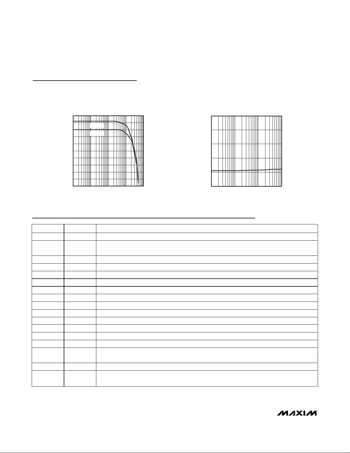
Typical Operating Characteristics (continued)
(AVDD= +5V, DVDD= 3.3V, R
LOAD
= 150Ω to GND, CIN= 0.1µF, TA= +25°C.)
Pin Description
BYPASS-MODE FREQUENCY RESPONSE
10
5
0
-5
-10
-15
-20
RESPONSE (dB)
-25
-30
-35
-40
0.1 101 100 1000
MAX7473
MAX7472
FREQUENCY (MHz)
PIN NAME FUNCTION
1 INC1 Channel C Input 1. AC-couple INC1 with a series 0.1µF capacitor.
2, 6, 25, 26 AGND
Analog Ground. Connect all AGND pins to the ground plane. See the Power-Supply Bypassing and
Layout Considerations section.
3 INA2 Channel A Input 2. AC-couple INA2 with a series 0.1µF capacitor.
4 INB2 Channel B Input 2. AC-couple INB2 with a series 0.1µF capacitor.
5 INC2 Channel C Input 2. AC-couple INC2 with a series 0.1µF capacitor.
7 INA3 Channel A Input 3. AC-couple INA3 with a series 0.1µF capacitor.
8 INB3 Channel B Input 3. AC-couple INB3 with a series 0.1µF capacitor.
9 INC3 Channel C Input 3. AC-couple INC3 with a series 0.1µF capacitor.
10 DGND Digital Ground. See the Power-Supply Bypassing and Layout Considerations section.
11 SYNCA Channel A External Sync Input. Connect to ground if not used.
12 SYNCB Channel B External Sync Input. Connect to ground if not used.
13 SYNCC Channel C External Sync Input. Connect to ground if not used.
14 SCL I2C-Compatible Serial Clock Input
15 SDA I2C-Compatible Serial Data Input/Output
16 DV
DD
Digital Power Supply. Bypass to DGND with a 0.1µF capacitor. See the Power-Supply Bypassing and
Layout Considerations section.
17 OUT3 Video Output 3. OUT3 can be either AC- or DC-coupled.
18, 20, 22 AV
DD
Analog Power Supply. Bypass each AVDD input to AGND using a 0.1µF capacitor. See the Power-
Supply Bypassing and Layout Considerations section.
MAX7472/73 toc10
BYPASS-MODE GROUP DELAY
20
16
12
DELAY (ns)
8
4
0
0.1 101100
FREQUENCY (MHz)
MAX7472/73 toc11
Page 7

MAX7472/MAX7473
HDTV Anti-Aliasing Filters with Triple-Input Mux
_______________________________________________________________________________________ 7
Pin Description (continued)
Detailed Description
The MAX7472/MAX7473 are complete video anti-aliasing solutions ideal for fixed-pixel HDTV display technologies such as plasma and LCD, which digitize the
input video signal and then scale the resolution to
match the native pixel format of the display. With a software-selectable corner frequency ranging from 5MHz
to 34MHz, the MAX7472/MAX7473 support both SD
and HD video signals including 1080i, 720p, 720i,
480p, and 480i. Higher bandwidth computer resolution
signals are also supported.
Integrated lowpass filters limit the analog video input
bandwidth for anti-aliasing and out-of-band noise
reduction prior to sampling by an ADC or video
decoder. By allowing the corner frequency to be adjusted from below SD resolution to beyond HD resolutions
in 256 steps, the filter’s corner frequency can be optimized dynamically for a specific input video signal and
the sampling frequency of the ADC or video decoder.
The MAX7472/MAX7473 provide a filter-bypass mode
to support applications requiring a passband greater
than 34MHz.
An I2C interface allows a microcontroller to configure
the MAX7472/MAX7473s’ performance and functionality
including the mux, the clamp voltage, the filter’s corner
frequency, the sync source (internal/external), and filter
bypassing.
The
Typical Operating Circuit
shows the block diagram
and typical external connections of the MAX7472/
MAX7473.
Sync Detector and Clamp Levels
The MAX7472/MAX7473 use a video clamp circuit to
establish a DC offset for the incoming video signal after
the AC-coupling capacitor. This video clamp sets the DC
bias level of the circuit at the optimum operating point.
The MAX7472/MAX7473 support both internal and
external sync detection. Selection of internal vs. external detection is achieved by programming the command byte (see Table 3). After extracting the sync
information from channel 1 or an external sync (SYNCA,
SYNCB, or SYNCC), the MAX7472/MAX7473 clamp the
video signal during the sync tip portion of the video.
Select one of two possible clamp levels according to
the input signal format. Use the low level when the input
signal contains sync information such as Y (luma) or
CVBS signals. Use the high level for bipolar signals
such as C (chroma) or PB/PR. See Table 1.
Table 1. Clamp Levels
PIN NAME FUNCTION
19 OUT2 Video Output 2. OUT2 can be either AC- or DC-coupled.
21 OUT1 Video Output 1. OUT1 can be either AC- or DC-coupled.
23 A0 Address Bit 0
24 A1 Address Bit 1
27 INA1 Channel A Input 1. AC-couple INA1 with a series 0.1µF capacitor.
28 INB1 Channel B Input 1. AC-couple INB1 with a series 0.1µF capacitor.
Exposed Pad. The exposed pad is located on the package bottom and is internally connected to
—EP
AGND. Connect EP to the analog ground plane. Do not route any PC board traces under the
package. See the Power-Supply Bypassing and Layout Considerations section.
INPUT SIGNAL FORMAT
Y PB P
R
GsBR Low High High
CVBS Y C Low Low High
Y PB PR (sync on all signals) Low Low Low
R G B H V High High High
CLAMP LEVEL
CHANNEL 1 CHANNEL 2 CHANNEL 3
Low High High
Page 8

MAX7472/MAX7473
Component/Composite Selection
The MAX7472/MAX7473 accept component or composite inputs. The sync detection path provides an
additional selectable color burst filter to improve sync
detection.
External Sync Detection
When filtering a video signal without embedded sync
information, such as computer formats (RGBHV) with
separate sync signals, use the external sync mode (see
Table 3) and apply the horizontal sync source to the
SYNCA, SYNCB, or SYNCC pin. The sync detector
determines when the clamp circuit is turned on.
The MAX7472/MAX7473 can detect positive or negative polarity external syncs with TTL logic levels. Use
the I2C interface to program the polarity of the external
sync signal.
Filter
The internal video filter delivers an optimized response
with a steep transition band to achieve a wide passband along with excellent stopband rejection. In addition, the filter is optimized to provide an excellent timedomain response with low overshoot.
Setting the Filter Frequency
The frequency response (-3dB cutoff frequency) of the
filter in the MAX7472/MAX7473 can be varied from less
than the SD passband to beyond the HD passband in
256 linear steps through the I2C interface. Use the command byte to write to the Frequency register followed
by the 8-bit data word that corresponds to the desired
frequency. See Table 6.
The Frequency register sets the -3dB point. Set this frequency accordingly to achieve the desired flat passband response.
Optimizing the Frequency Response
Select the frequency according to the resolution of the
video-signal format. High-definition signals require
higher bandwidth and standard-definition signals
require less bandwidth. The actual bandwidth contained in the video signal is a function of the visual resolution of the signal. This bandwidth is typically less
than what is indicated by the format resolution (1080i,
720p, 480p, and 480i). For more information on this
topic, see Application Note 750:
Bandwidth vs. Video
Resolution
on the Maxim website (www.maxim-ic.com).
See Table 6.
The frequency response can be optimized to improve
the overall performance. There are a number of consid-
erations, one of the most important being the sampling
rate of the subsequent ADC or video decoder in the
system. In oversampled systems, the sampling rate is
significantly more than the desired passband response.
The extra frequency span between the passband and
the sampling rate contains noise that can be eliminated
by setting the corner frequency of the filter to just pass
the desired bandwidth. This results in a higher signalto-noise ratio of the overall system.
Filter Bypass
The MAX7472/MAX7473 offer selectable filter bypassing that allows the input video signals to bypass the
internal filters reaching the output buffers unfiltered.
The filter-bypass mode is enabled/disabled through the
command byte (see Table 3).
Output Buffer
Each output buffer can drive a 2V
P-P
signal into a 150Ω
video load. The MAX7472/MAX7473 can drive a DC- or
AC-coupled load. The output DC level is controlled to
limit the DC voltage on the cable so that the blanking
level of the video signal is always less than 1V, meeting
the digital TV specification. As a result, output AC-coupling capacitors can be eliminated when driving a
cable, thus eliminating the normal adverse effects
caused by these capacitors such as line- and field-time
distortion, otherwise known as droop. See the
Output
Considerations
section for more information.
Gain Options
The MAX7472 features an overall gain of 0dB, while the
MAX7473 features an overall gain of +6dB. Use the
+6dB option (MAX7473) when driving a back-matched
cable. Use the 0dB option (MAX7472) when driving an
ADC or video decoder with an input range the same as
the input to the MAX7472. To add flexibility, the
MAX7472 accepts input signals up to 2V
P-P
, twice the
standard video-signal range.
Output Clamp Level
The MAX7472/MAX7473 output can be DC- or AC-coupled. The nominal output clamp level in the DC-coupled case depends on the clamp voltage setting and
can be determined according to Table 2.
HDTV Anti-Aliasing Filters with Triple-Input Mux
8 _______________________________________________________________________________________
Table 2. Output Clamp Level
CLAMP SETTING
Low ±100
High ±100
OUTPUT CLAMP LEVEL (mV)
(typ)
Page 9

As shown in the
Sync Detector and Clamp Levels
section, the low clamp level is used for signals with sync
information and determines the voltage level of the
sync tip, while the high clamp level is used for signals
without sync information and sets the blanking level.
The absolute voltage level of the output signal is relative to the output clamp level. A video signal containing
sync information (i.e., CVBS or Y) is unipolar above the
clamp level and conversely, a video signal without sync
(i.e., PB, PR, or C) is bipolar around the clamp level.
Multiplexers
The MAX7472/MAX7473 provide four 3:1 multiplexers
programmable through the I2C interface to select which
of three separate channels (channels A, B, C) is to be
connected to each video input. The fourth multiplexer is
used in conjunction with external sync detection and
determines which channel’s external sync is to be connected to the external sync input.
See Table 3 and the
Serial Interface
section for more
information on how to select a particular channel. After
selecting a channel with a command byte, bits CS7
and CS6 of the Channel Selection register reflect the
channel setting (Table 7).
Power-Down Mode
The MAX7472/MAX7473 include a power-down mode
that reduces the supply current from 180mA (typ) to
1mA (typ) by powering down the analog circuitry. The
I2C interface remains active allowing the device to
return to full-power operation. The clamp settling time
(see the
Electrical Characteristics
table) limits the
wake-up time of the MAX7472/MAX7473. After exiting
the power-down mode, the MAX7472/MAX7473 resume
normal operation using the settings stored prior to
power-down. The command byte controls the powerdown and wake-up modes (see Table 3). A software
reset sets the Control/Status register to its default conditions. The Frequency register and the Channel
Selection register are not affected.
Power-On Reset (POR)
The MAX7472/MAX7473 include a power-on reset
(POR) circuit that resets the internal registers and I2C
interface to their default condition (see Tables 4–7).
Serial Interface
The MAX7472/MAX7473 feature an I2C-compatible,
2-wire serial interface consisting of a bidirectional serial
data line (SDA) and a serial clock line (SCL). SDA and
SCL facilitate bidirectional communication between the
MAX7472/MAX7473 and the master at rates up to 400kHz.
Once a command byte is written to the MAX7472/
MAX7473, the command interpreter changes the
Control/Status register and the Channel Selection register accordingly. See the
Control/Status Register
and
Channel-Selection Register
sections for more information. The command interpreter also controls access to
the Frequency register (see the
Command Byte (Write
Cycle)
section).
The MAX7472/MAX7473 are transmit/receive slave-only
devices, relying upon a master to generate a clock signal. The master (typically a microcontroller) initiates
data transfer on the bus and generates SCL.
A master device communicates to the MAX7472/
MAX7473 by transmitting the proper address (see the
Slave Address
section) followed by a command and/or
data words. Each transmit sequence is framed with a
START (S) or REPEATED START (Sr) condition and a
STOP (P) condition.
The SDA driver is an open-drain output, requiring a
pullup resistor (2.4kΩ or greater) to generate a logichigh voltage. Optional resistors (24Ω) in series with
SDA and SCL protect the device inputs from high-voltage spikes on the bus lines. Series resistors also minimize crosstalk and undershoot of the bus signals.
Bit Transfer
Each SCL rising edge transfers 1 data bit. Nine clock
cycles are required to transfer the data into or out of the
MAX7472/MAX7473. The data on SDA must remain stable
during the high period of the SCL clock pulse. Changes in
SDA while SCL is high are read as control signals (see the
START and STOP Conditions
section). When the serial
interface is inactive, SDA and SCL idle high.
START and STOP Conditions
A master device initiates communication by issuing a
START condition (S), a high-to-low transition on SDA with
SCL high (Figure 2). The master terminates transmission
by a STOP condition (P) (see the
Acknowledge Bit (ACK)
and Not-Acknowledge Bit (NACK)
section). A STOP condition is a low-to-high transition on SDA while SCL is high
(Figure 2). The STOP condition frees the bus. If a repeated START condition (Sr) is generated instead of a STOP
condition, the bus remains active. When a STOP condition or incorrect address is detected, the MAX7472/
MAX7473 then ignore all communication on the I
2
C bus
until the next START or REPEATED START condition,
minimizing digital noise and feedthrough.
MAX7472/MAX7473
HDTV Anti-Aliasing Filters with Triple-Input Mux
_______________________________________________________________________________________ 9
Page 10

MAX7472/MAX7473
Early STOP Conditions
The MAX7472/MAX7473 recognize a STOP condition at
any point during transmission except when a STOP
condition occurs in the same high pulse as a START
condition (Figure 3). This condition is not a legal I2C
format; at least one clock pulse must separate any
START and STOP conditions. The MAX7472/MAX7473
discard any data received during a data transfer aborted by an early STOP condition.
REPEATED START (Sr) Conditions
An Sr condition is used to indicate a change in direction of data flow (see the
Read Cycle
section). Sr can
also be used when the bus master is writing to several
I2C devices and does not want to relinquish control of
the bus. The MAX7472/MAX7473 serial interface supports continuous write operations with (or without) an Sr
condition separating them.
Acknowledge Bit (ACK) and
Not-Acknowledge Bit (NACK)
Successful data transfers are acknowledged with an
acknowledge bit (ACK) or a not-acknowledge bit
(NACK). Both the master and the MAX7472/MAX7473
(slave) generate acknowledge bits. To generate an
acknowledge, the receiving device must pull SDA low
before the rising edge of the acknowledge-related clock
pulse (ninth pulse) and keep it low during the high period
of the clock pulse (Figure 4). To generate a not acknowledge, the receiver allows SDA to be pulled high before
the rising edge of the acknowledge-related clock pulse
(ninth pulse) and leaves it high during the high period of
the clock pulse. Monitoring the acknowledge bits allows
for detection of unsuccessful data transfers. An unsuccessful data transfer happens if a receiving device is
busy or if a system fault has occurred. In the event of an
unsuccessful data transfer, the master should reattempt
communication at a later time.
The MAX7472/MAX7473 generate an acknowledge bit
when receiving an address or data by pulling SDA low
during the ninth clock pulse. When transmitting data
during a read, the MAX7472/MAX7473 do not drive
SDA during the ninth clock pulse (i.e., the external
pullups define the bus as a logic high) so that the
receiver of the data can pull SDA low to acknowledge
receipt of data.
Slave Address
A bus master initiates communication with a slave device
by issuing a START condition followed by the 7-bit slave
address (Figure 5). When idle, the MAX7472/MAX7473
wait for a START condition followed by its slave address.
The serial interface compares each address bit by bit,
allowing the interface to power down and disconnect
from SCL immediately if an incorrect address is detected. After recognizing a START condition followed by the
correct address, the MAX7472/MAX7473 are ready to
accept or send data. The least significant bit (LSB) of the
address byte (R/W) determines whether the master is
writing to or reading from the MAX7472/MAX7473 (R/W =
0 selects a write condition, R/W = 1 selects a read condi-
HDTV Anti-Aliasing Filters with Triple-Input Mux
10 ______________________________________________________________________________________
Figure 2. START/STOP Conditions
Figure 3. Early STOP Conditions
Figure 4. Acknowledge and Not-Acknowledge Bits
SPSr
SCL
SDA
LEGAL STOP CONDITION
SCL
SDA
STARTSTOP
S
SDA
SCL
189
ILLEGAL STOP CONDITION
SCL
SDA
START
NOT ACKNOWLEDGE
ACKNOWLEDGE
ILLEGAL
STOP
Page 11

tion). After receiving the proper address, the
MAX7472/MAX7473 (slave) issue an ACK by pulling
SDA low for one clock cycle.
The MAX7472/MAX7473 slave address consists of 5
fixed bits A6–A2 (set to 10010) followed by 2 pin-programmable bits A1 and A0. The most significant address
bit (A6) is transmitted first, followed by the remaining
bits. Addresses A1 and A0 can also be driven dynamically if required, but the values must be stable when they
are expected in the address sequence.
Command Byte (Write Cycle)
A write cycle begins with the bus master issuing a
START condition followed by 7 address bits (Figure 5)
and a write bit (R/W = 0). After successfully receiving
its address, the MAX7472/MAX7473 (slave) issue an
ACK. The MAX7472/MAX7473 recognize the next byte
after a successfully received address as the command
byte (Table 3).
Use the command byte to configure the MAX7472/
MAX7473. While most of the commands listed in Table
3 modify the functionality of the MAX7472/
MAX7473, some commands prepare the device for further data transfers (see the
Control/Status Register
,
Frequency Register
, and
Channel-Selection Register
sections.) When the write cycle is prematurely aborted,
the register is not updated. Figures 6 and 7 show
examples of write sequences.
MAX7472/MAX7473
HDTV Anti-Aliasing Filters with Triple-Input Mux
______________________________________________________________________________________ 11
Figure 5. Slave-Address Byte Definition
Figure 6. Write Sequence to Update the Frequency Register
SDA
SCL
1 0 1 0 A1 A00 R/W
MSB LSB
ACK
SCL
SDA
SDA
DIRECTION
SCL (CONT)
SDA (CONT)
SDA
DIRECTION
COMMAND WORD C7–C0 IS 00010010.
1 0 0 1 0 A1 A0 R/W
START
F7 F6 F5 F4 F3 F2 F1 ACK
IN IN
00010010
ACK ACK
C7 C6 C5 C4 C3 C2 C1 C0
F0
OUT
STOP
OUTINOUTIN TO MAX7472/MAX7473
Page 12

MAX7472/MAX7473
HDTV Anti-Aliasing Filters with Triple-Input Mux
12 ______________________________________________________________________________________
Table 3. Command Byte Definition
COMMAND BYTE: INDIVIDUAL BIT DEFINITIONS
C7 C6 C5 C4 C3 C2 C1 C0
0 0 0 0 0 0 0 0 Power-down.
00000001
0 0 0 0 0 0 1 0 Set clamp voltage level for IN1 to low.
0 0 0 0 0 0 1 1 Set clamp voltage level for IN1 to high.
0 0 0 0 0 1 0 0 Set clamp voltage level for IN2 to low.
0 0 0 0 0 1 0 1 Set clamp voltage level for IN2 to high.
0 0 0 0 0 1 1 0 Set clamp voltage level for IN3 to low.
0 0 0 0 0 1 1 1 Set clamp voltage level for IN3 to high.
0 0 0 0 1 0 0 0 Select component input, color-burst filter disabled.
0 0 0 0 1 0 0 1 Select composite input, color-burst filter enabled.
0 0 0 0 1 0 1 0 Select internal sync.
0 0 0 0 1 0 1 1 Select external sync.
0 0 0 0 1 1 0 0 Select positive polarity for the external sync.
0 0 0 0 1 1 0 1 Select negative polarity for the external sync.
0 0 0 0 1 1 1 0 Enable filters.
0 0 0 0 1 1 1 1 Disable filters. Enter bypass mode.
00010000
00010001
0 0 0 1 0 0 1 0 Load the Frequency register with the data byte following the command word.
00010011
0 0 0 1 0 1 0 0 Select Input A.
0 0 0 1 0 1 0 1 Select Input B.
0 0 0 1 0 1 1 0 Select Input C.
00010111
Wake-up; resume normal operation using the frequency/status previously
stored (unless power has been cycled).
Reset status to the default status as outlined in the Control/Status register
table. This command does not affect the Frequency register and the Channel
Selection register.
Request reading the Control/Status register. The interface expects an Sr
condition to follow with address and read/write set to read so that data can be
driven onto the bus.
Request reading the Frequency register. The interface expects an Sr
condition to follow with address and read/write set to read so that data can be
driven onto the bus.
Request reading the Channel Selection register. The interface expects an Sr
condition to follow with address and read/write set to read so that data can be
driven onto the bus.
DESCRIPTION
Page 13

Read Cycle
In read mode (R/W = 1), the MAX7472/MAX7473 write
the contents of the Status, Channel Selection, or
Frequency register to the bus. When the command
byte indicates a read operation of either the Status or
the Frequency register, the serial interface expects an
Sr condition to follow the command byte. After sending
an Sr, the master sends the MAX7472/MAX7473 slave
address byte followed by the R/W bit (set to 1 to indicate a read). The slave device (MAX7472/MAX7473)
generates an ACK for the second address word and
immediately after the ACK clock pulse, the direction of
data flow reverses. The slave (MAX7472/MAX7473)
then transmits 1 byte of data containing the value of the
register that was selected in the command byte. Figure
8 shows a basic read sequence.
Note: To read the contents of the Status, Channel
Selection, or Frequency register, the master must first
write a command byte, requesting to read the Status,
Channel Selection, or Frequency register.
MAX7472/MAX7473
HDTV Anti-Aliasing Filters with Triple-Input Mux
______________________________________________________________________________________ 13
Figure 7. Write Sequence for a Command Bite
Figure 8. Basic Read Sequence
SCL
SDA
SDA
DIRECTION
COMMAND BITE IS FOR POWER-DOWN.
1 0 0 1 0 A1 A0 R/W
START
SCL
SDA
SDA
DIRECTION
SCL (CONT)
1 0 0 1 0 A1 A0 R/W
START
ACK ACK
00000000
C7 C6 C5 C4 C3 C2 C1 C0
ACK
0 0 0 1 0 0 1/0 1
C7 C6 C5 C4 C3 C2 C1 C0
OUTIN INOUTIN TO MAX7472/MAX7473
STOP
ACK
OUTINOUTIN TO MAX7472/MAX7473
SDA (CONT)
SDA
DIRECTION
Sr
IN IN
ACK
R/W
D71 D6 D5 D4 D3 D2 D1 ACK
OUT
D0000 1 A1 A0
STOP
Page 14

MAX7472/MAX7473
Control/Status Register
The MAX7472/MAX7473 store their status in an 8-bit
register that can be read back by the master. The individual bits of the Control/Status register are summarized in Tables 4 and 5. The power-on default value of
this register is 03h.
Frequency Register
The frequency response (-3dB passband edge) of the
MAX7472/MAX7473 can be continuously varied in 256
linear steps by changing the codes in the Frequency
register (Table 6). See the
Command Byte(Write Cycle)
section for a write sequence to update the Frequency
register.
HDTV Anti-Aliasing Filters with Triple-Input Mux
14 ______________________________________________________________________________________
Table 4. Control/Status Register
Table 5. Control/Status Register Bit Description
Table 6. Suggested Frequency Register Setting for Various Video-Signal Formats
S7 S6 S5 S4 S3 S2 S1 S0
CONTROL/STATUS REGISTER
BIT DESCRIPTION
S7
S6
S5
S4
S3
S2
S1
S0
0 = component input signal selected (default).
1 = composite input signal selected.
0 = internal sync enabled (default).
1 = external sync enabled.
0 = external sync: positive polarity (default).
1 = external sync: negative polarity.
0 = normal operation mode (default).
1 = power-down mode.
0 = filters enabled (default).
1 = bypass mode—no filtering.
0 = clamp voltage for IN1 set to low (default).
1 = clamp voltage for IN1 set to high.
0 = clamp voltage for IN2 set to low.
1 = clamp voltage for IN2 set to high (default).
0 = clamp voltage for IN3 set to low.
1 = clamp voltage for IN3 set to high (default).
VIDEO-SIGNAL
FORMAT
Standard-Definition
Interlaced
Standard-Definition
Progressive
High-Definition Low
Bandwidth
High-Definition High
Bandwidth
F7 F6 F5 F4 F3 F2 F1 F0 CODE NUMBER
00101000 40 10
01011010 90 15
11011100 220 30
11111111 255 34 (default)
APPROXIMATE
FREQUENCY
(-3dB) (MHz)
Page 15

Channel-Selection Register
The MAX7472/MAX7473 store channel selection in an
8-bit register that can be read back by the master. The
individual bits of the Channel Selection register are
summarized in Table 7. The power-on default selects
channel A.
I2C Compatibility
The MAX7472/MAX7473 are compatible with existing
I2C systems supporting standard I2C 8-bit communications. The general call address is ignored, and CBUS
formats are not supported. The devices’ address is
compatible with 7-bit I2C addressing protocol only.
Ten-bit address formats are not supported.
Applications Information
Input Considerations
Use 0.1µF ceramic capacitors to AC-couple the inputs.
The input cannot be DC-coupled. The internal clamp
circuit stores a DC voltage across the input capacitors
to obtain the appropriate output DC voltage level.
Increasing the value of these capacitors to improve
line-time distortion is not necessary due to the extremely low input leakage current yielding a very low line-time
distortion performance.
The MAX7472/MAX7473 provide a high input impedance to allow a nonzero source impedance to be used
such as when the input is connected directly to a back-
matched video cable, ensuring the external resistance
determines the termination impedance.
Output Considerations
The MAX7472/MAX7473 outputs can be DC- or ACcoupled. The MAX7473, with +6dB gain, is typically
connected to a 75Ω series back-match resistor followed by the video cable. Because of the inherent
divide-by-two of this configuration, the blanking level of
the video signal is always less than 1V, which complies
with digital TV requirements.
The MAX7472, with 0dB gain, is typically connected to
an ADC or video decoder. This can be a DC or AC connection. If a DC connection is used, ensure that the DC
input requirements of the ADC or video decoder are
compatible.
When using an AC connection, choose an AC-coupling
capacitor value that ensures that the lowest frequency
content in the video signal is passed and the line-time
distortion is kept within desired limits. The selection of
this value is a function of the input impedance and more
importantly, the input leakage of the circuit being driven.
Use a video clamp to reestablish the DC level if not
already included in the subsequent circuit.
The outputs of the MAX7472/MAX7473 are fully protected against short-circuit conditions either to ground or to
the positive supply of the device.
MAX7472/MAX7473
HDTV Anti-Aliasing Filters with Triple-Input Mux
______________________________________________________________________________________ 15
Table 7. Channel-Selection Register
X = Don’t care.
CHANNEL-SELECTION REGISTER
CS7 CS6 CS5 CS4 CS3 CS2 CS1 CS0
00XXXXXXChannel A selected (default).
01XXXXXXChannel B selected.
10XXXXXXChannel C selected.
DESCRIPTION
Page 16

MAX7472/MAX7473
Power-Supply Bypassing and
Layout Considerations
The MAX7472/MAX7473 operate from a single +5V
analog supply and +3.3V digital supply. Bypass each
AVDDto AGND with a 0.1µF capacitor with an additional 1µF capacitor in parallel for low-frequency decoupling. Determine the proper power-supply bypassing
necessary by taking into account the desired disturbance level tolerable on the output, the power-supply
rejection of the MAX7472/MAX7473, and the amplitude
and frequency of the disturbance signals present in the
vicinity of the MAX7472/MAX7473. Use an extensive
ground plane to ensure optimum performance. The
three AV
DD
inputs (pins 18, 20, and 22) that supply the
individual channels can be connected together and
bypassed as one provided the components are close
to the pins. Bypass DVDDto DGND with a 0.1µF capacitor. Connect all ground pins to a low-impedance
ground plane as close to the device as possible.
Place the input termination resistors as close to the
device as possible. Alternatively, the terminations can
be placed further from the device if the PC board
traces are designed to be a controlled impedance of
75Ω. Minimize parasitic capacitance as much as possible to avoid performance degradation in the upper frequency range possible with the MAX7472/MAX7473.
Refer to the MAX7472/MAX7473 evaluation kit for a
proven PC board layout.
Exposed Pad and Heat Dissipation
The MAX7472/MAX7473 TQFN package provides an
exposed pad on the bottom side of the package. This
pad is electrically connected to AGND and must be
soldered to the ground plane for proper thermal conductivity. Do not route any PC board traces under the
package.
The MAX7472/MAX7473 typically dissipate 900mW of
power; therefore, pay attention to heat dispersion. Use
at least a two-layer board with a good ground plane. To
maximize heat dispersion, place copper directly under
the MAX7472/MAX7473 package to match the outline
of the plastic encapsulated area. Repeat the same with
the bottom ground plane layer and place as many vias
as possible connecting the top and bottom layers to
thermally connect to the ground plane.
Maxim has evaluated a four-layer board using FR-4
material and 1oz copper with equal areas of metal on
the top and bottom side coincident with the plastic
encapsulated areas of the package. The two middle
layers are used as power and ground planes. The
board has 21, 15-mil, plated-through via holes between
top, bottom, and ground plane layers. Thermocouple
measurements confirm device temperatures to be safely within maximum limits.
HDTV Anti-Aliasing Filters with Triple-Input Mux
16 ______________________________________________________________________________________
Page 17

MAX7472/MAX7473
HDTV Anti-Aliasing Filters with Triple-Input Mux
______________________________________________________________________________________ 17
Typical Operating Circuit
Chip Information
PROCESS: BiCMOS
VGA
AV
DD
0.1μF
INA1
INA2
HD
SD
INA3
SYNCA
INB1
INB2
INB3
SYNCB
INC1
INC2
INC3
SYNCC
MAX7472
(MAX7473)
MUX MUX
MUX MUX
EXT SYNC
ENABLE
CLAMP/
BIAS
CLAMP/
BIAS
INTERFACE
I
2
C
PROGRAMMABLE
LPF FILTER
5MHz–34MHz
3
PROGRAMMABLE
LPF FILTER
5MHz–34MHz
PROGRAMMABLE
LPF FILTER
5MHz–34MHz
CLAMP LEVEL
BYPASS
DV
DD
0.1μF
2
0dB (6dB)
BUFFER
0dB (6dB)
BUFFER
0dB (6dB)
BUFFER
OUT1
OUT2
OUT3
0.1μF
0.1μF
ADCCLAMP
ADC
ADC
() INDICATES THE MAX7473
AGND
SDA A1 A0
SCL
DGND
Page 18

MAX7472/MAX7473
HDTV Anti-Aliasing Filters with Triple-Input Mux
18 ______________________________________________________________________________________
Package Information
(The package drawing(s) in this data sheet may not reflect the most current specifications. For the latest package outline information
go to www.maxim-ic.com/packages
.)
24L QFN THIN.EPS
PACKAGE OUTLINE,
12, 16, 20, 24, 28L THIN QFN, 4x4x0.8mm
21-0139
1
E
2
Page 19

MAX7472/MAX7473
HDTV Anti-Aliasing Filters with Triple-Input Mux
Maxim cannot assume responsibility for use of any circuitry other than circuitry entirely embodied in a Maxim product. No circuit patent licenses are
implied. Maxim reserves the right to change the circuitry and specifications without notice at any time.
Maxim Integrated Products, 120 San Gabriel Drive, Sunnyvale, CA 94086 408-737-7600 ____________________
19
© 2006 Maxim Integrated Products is a registered trademark of Maxim Integrated Products, Inc.
Package Information (continued)
(The package drawing(s) in this data sheet may not reflect the most current specifications. For the latest package outline information
go to www.maxim-ic.com/packages
.)
PACKAGE OUTLINE,
12, 16, 20, 24, 28L THIN QFN, 4x4x0.8mm
21-0139
2
E
2
 Loading...