

Page 1
19-0171; Rev 1; 9/93
High-Efficiency PWM, Step-Down
P-Channel DC-DC Controller
_______________General Description
The MAX747 high-efficiency, high-current, step-down
controller drives external P-channel FETs. It provides
90% to 95% efficiency from a 6V supply with load
currents ranging from 50mA up to 2.5A. It uses a
pulse-width-modulating (PWM) current-mode control
scheme to provide precise output regulation and low
output noise. The MAX747’s 4V to 15V input voltage
range, a fixed 5V/adjustable (Dual-Mode™) output, and
a current limit set with an external resistor make this
device ideal for a wide range of applications.
High efficiency is maintained with light loads due to a
proprietary dual-control (Idle-Mode™) scheme that
minimizes switching losses by reducing the switching
frequency at light loads. The low 800µA quiescent
current and ultra-low 0.6µA shutdown current further
extend battery life.
External components are protected by the MAX747’s
cycle-by-cycle current limit. The MAX747 also features a
2V ±1.5% reference, a comparator for low-battery
detection or level translating, as well as soft-start and
shutdown capability.
The MAX746, discussed in a separate data sheet,
functions similarly to the MAX747, but it drives N-channel
logic level FETs on the high side.
________________________Applications
Notebook Power Supplies
Personal Digital Assistants
Battery-Operated Equipment
Cellular Phones
5V to 3.3V Green PC Applications
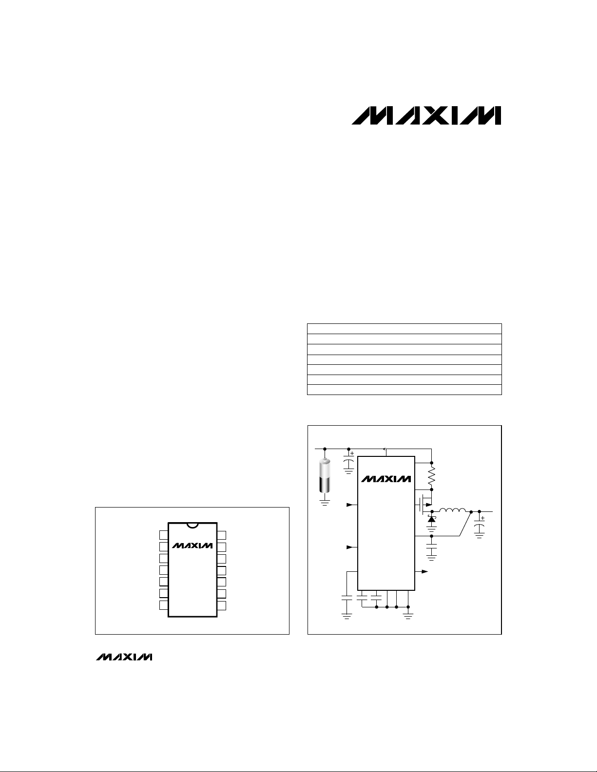
__________________Pin Configuration
TOP VIEW
LBI
REF
SHDN
AV+
1
2
SS
MAX747
3
4
FB
5
CC
6
7
LBO
14
GND
13
12
V+
EXT
11
AGND
10
CS
9
OUT
8
____________________________Features
♦ 90% to 95% Efficiency for 50mA to 2.5A
Output Currents
♦ 4V to 15V Input Voltage Range
♦ Low 800µA Supply Current
♦ 0.6µA Shutdown Current
♦ Drives External P-Channel FETs
♦ Cycle-by-Cycle Current Limiting
♦ 2V ±1.5% Accurate Reference Output
♦ Adjustable Soft-Start
♦ Precision Comparator for Power-Fail or
Low-Battery Warning
______________Ordering Information
PART TEMP. RANGE PIN-PACKAGE
MAX747CPD 0°C to +70°C 14 Plastic DIP
MAX747CSD 0°C to +70°C 14 Narrow SO
MAX747C/D 0°C to +70°C Dice*
MAX747EPD -40°C to +85°C 14 Plastic DIP
MAX747ESD -40°C to +85°C 14 Narrow SO
MAX747MJD -55°C to +125°C 14 CERIDIP
* Contact factory for dice specifications.
__________Typical Operating Circuit
INPUT
6V TO 15V
V+
100µF
LOW-BATTERY
DETECTOR
INPUT
ON/OFF
MAX747
SHDN
LBI
REF
AV+
5OmΩ
CS
EXT
OUT
LBO
GND
AGNDFBCCSS
P
0.1µF
LOW-BATTERY
DETECTOR
OUTPUT
5OµH
OUTPUT
5V
2.3A
430µF
MAX747
DIP/SO
™ Dual-Mode and Idle-Mode are trademarks of Maxim Integrated Products.
________________________________________________________________
Maxim Integrated Products
Call toll free 1-800-998-8800 for free samples or literature.
1
Page 2
High-Efficiency PWM, Step-Down
P-Channel DC-DC Controller
ABSOLUTE MAXIMUM RATINGS
Supply Voltage V+, AV+ to GND..............................-0.3V to 17V
AGND to GND..........................................................-0.3V to 0.3V
All Other Pins................................................-0.3V to (V+ + 0.3V)
Reference Current (I
Continuous Power Dissipation (T
Plastic DIP (derate 10.00mW/°C above +70°C) ..........800mW
SO (derate 8.33mW/°C above +70°C).........................667mW
MAX747
CERDIP (derate 9.09mW/°C above +70°C).................727mW
Stresses beyond those listed under “Absolute Maximum Ratings” may cause permanent damage to the device. These are stress ratings only, and
functional operation of the device at these or any other conditions beyond those indicated in the operational sections of the specifications is not implied.
Exposure to absolute maximum rating conditions for extended periods may affect device reliability.
) ....................................................±2mA
REF
= +70°C)
A
ELECTRICAL CHARACTERISTICS
(V+ = 10V, I
Input Voltage Range V+ For regulated outputs 415V
Output Voltage V
Feedback Voltage
Line Regulation
Load Regulation 0V < V+ - CS < 0.125V 1.3 2.5 %
Efficiency Circuit of Figure 1, I
OUT Leakage Current V
FB Input Logic Low For dual-mode switchover 40 mV
FB Input Leakage Current FB = 2V 0.1 100 nA
Reference Voltage I
Reference Load Regulation I
Soft-Start Source Current SS = 0V 1 µA
Soft-Start Fault Current SS = 2V 100 500 µA
Supply Current
Oscillator Frequency f
Maximum Duty Cycle V+ = 6V 91 96 %
CS Amp I
EXT Output High I
EXT Output Low I
EXT Sink Current V
EXT Source Current V
CC Impedance 24 kΩ
LBI Threshold Voltage V
LBO Output Voltage Low I
LBI Input Leakage Current LBI = 2.5V 100 nA
LBO Output Leakage Current V+ = 15V, LBO = 15V, LBI = 2.5V 1 µA
SHDN Input Voltage Low V
SHDN Input Voltage High V
SHDN Input Leakage Current SHDN = 10V 0.1 100 nA
2 _______________________________________________________________________________________
= 0mA, I
LOAD
PARAMETER SYMBOL CONDITIONS MIN TYP MAX UNITS
Threshold V
LIM
= 0mA, TA= T
REF
to T
, unless otherwise noted.)
MAX
V+ = 6V to 15V, 0V < V+ - CS < 0.125V, FB = 0V
(includes line and load regulation)
V+ - CS = 0V, external
feedback mode
V+ = 6V to 15V, FB = 0V 0.05
V+ = 4V to 15V, external feedback mode 0.1
= 5V 50 80 µA
OUT
= 0µA
REF
= 0µA to 100µA 920mV
REF
Operating, V+ = 15V 0.95 1.3
Operating, V+ = 10V 0.8
Shutdown mode 0.6 20 µA
MAX747C 85 100 115
MAX747E/M 80 100 120
V+ - CS 125 150 175 mV
= -1mA (sourcing) V+ – 0.1 V
EXT
= 1mA (sinking) 0.25 V
EXT
= 7.5V 110 mA
EXT
= 2.5V 170 mA
EXT
LBI falling
= 0.5mA 0.4 V
SINK
OUT
V
REF
OSC
LIMIT
MIN
TH
IL
IH
Operating Temperature Ranges:
MAX747C_D .......................................................0°C to +70°C
MAX747E_D.....................................................-40°C to +85°C
MAX747MJD..................................................-55°C to +125°C
Junction Temperature
MAX747C_D/E_D.........................................................+150°C
MAX747MJD ...............................................................+175°C
Storage Temperature Range.............................-65°C to +160°C
Lead Temperature (soldering, 10sec).............................+300°C
4.85 5.08 5.25 V
MAX747C
MAX747E/M 1.95 2.00 2.05
= 0.5A to 2.5A 91 %
LOAD
MAX747C
MAX747E/M 1.96 2.00 2.04
MAX747C
MAX747EM 1.96 2.00 2.04
1.96 2.00 2.04
1.97 2.00 2.03
1.97 2.00 2.03
0.4 V
2.0 V
V
%V
V
mA
kHz
V
Page 3
High-Efficiency PWM, Step-Down
P-Channel DC-DC Controller
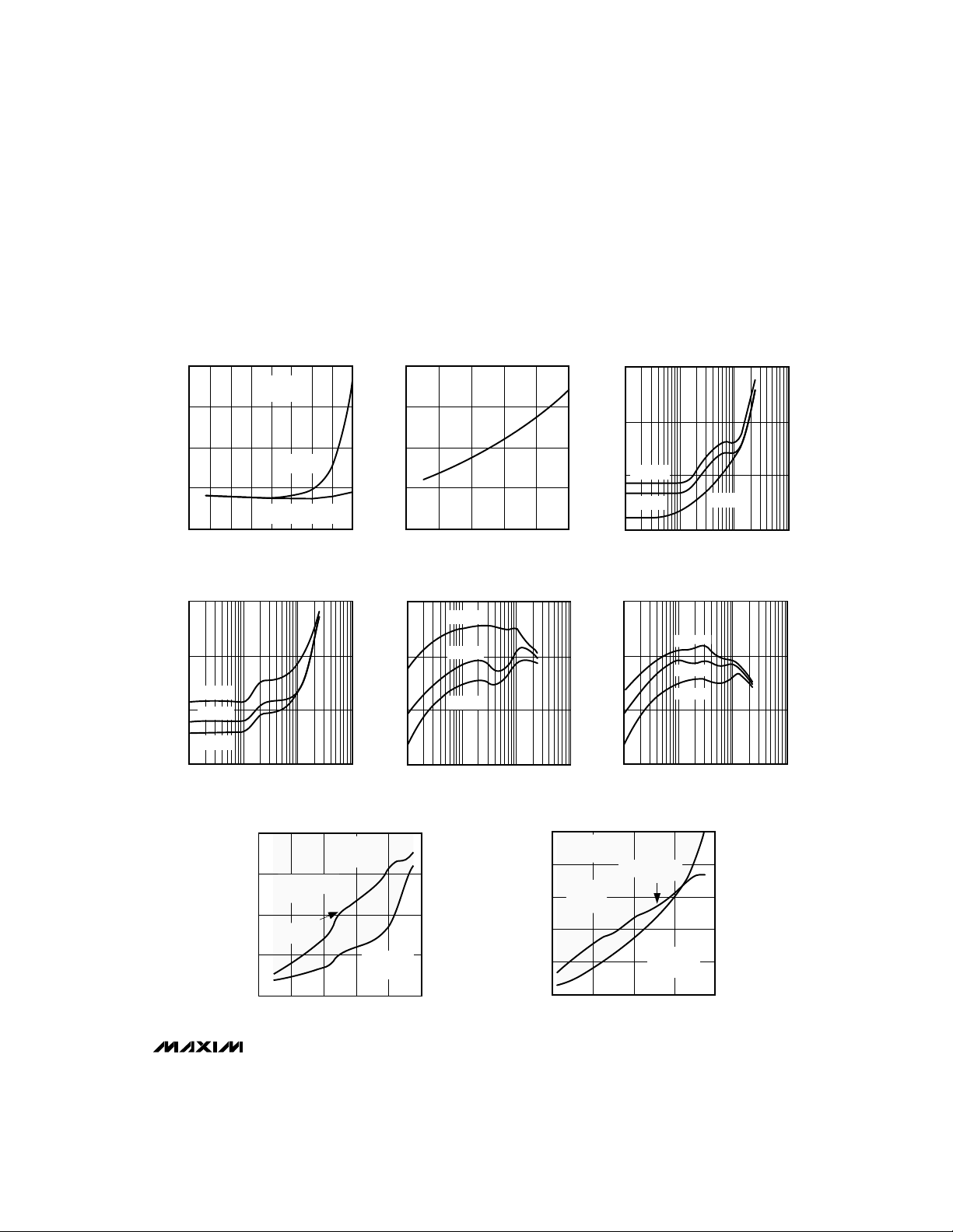
__________________________________________Typical Operating Characteristics
(Circuit of Figure 1, V+ = 9V, TA = +25°C, unless otherwise noted.)
SUPPLY CURRENT vs.
TEMPERATURE
4
3
2
1
SUPPLY CURRENT (mA)
0
-75
-50 -25 0 25 50 75 100 125
VIN = 9V
V
= 5V
OUT
ENTIRE
CIRCUIT
SCHOTTKY DIODE
LEAKAGE EXCLUDED
TEMPERATURE (°C)
PEAK INDUCTOR CURRENT vs.
OUTPUT CURRENT (V
3
2
VIN = 9V
1
VIN = 6V
PEAK INDUCTOR CURRENT (A)
VIN = 5V
0
0.01 0.1 10
OUTPUT CURRENT (A)
OUT
1
= 3.3V)
CONTINUOUS-CONDUCTION MODE BOUNDARY
AND CORRESPONDING PEAK INDUCTOR CURRENT (V
18
14
DISCONTINUOUS
CONDUCTION
REGION
10
SUPPLY VOLTAGE (V)
6
2
PEAK
INDUCTOR
CURRENT
0.6 1.0 1.4
0.4
0.8
OUTPUT CURRENT (A)
V
= 3.3V
OUT
L = 33µH
R
SENSE
1.0
MAX747-TOC1
0.9
0.8
0.7
SUPPLY CURRENT (mA)
0.6
100
MAX747-TOC6
90
EFFICIENCY (%)
80
70
= 50mΩ
CONTINUOUS
CONDUCTION
REGION
1.2
SUPPLY CURRENT vs.
SUPPLY VOLTAGE
5
71115
9
SUPPLY VOLTAGE (V)
13
EFFICIENCY vs. OUTPUT CURRENT
= 5V)
(V
OUT
VIN = 6V
VIN = 9V
VIN = 12V
0.01 0.1 10
OUTPUT CURRENT (A)
1
CONTINUOUS-CONDUCTION MODE BOUNDARY
= 3.3V)
OUT
2.0
PEAK INDUCTOR CURRENT (A)
MAX747-TOC3
1.6
1.2
0.8
0.4
AND CORRESPONDING PEAK INDUCTOR CURRENT (V
15
13
11
9
SUPPLY VOLTAGE (V)
7
5
0.5
PEAK INDUCTOR CURRENT vs.
OUTPUT CURRENT (V
3
MAX747-TOC2
2
VIN = 12V
1
VIN = 9V
PEAK INDUCTOR CURRENT (A)
0
0.01 0.1 10
OUTPUT CURRENT (A)
EFFICIENCY vs. OUTPUT CURRENT
100
MAX1747-TOC7
90
EFFICIENCY (%)
80
70
0.01 0.1 10
DISCONTINUOUS
CONDUCTION
REGION
V
= 5V
OUT
L = 50µH
R
= 50mΩ
SENSE
0.7 1.3
OUTPUT CURRENT (A)
OUTPUT CURRENT (A)
PEAK INDUCTOR
CURRENT
CONTINUOUS
CONDUCTION
REGION
(V
OUT
VIN = 6V
VIN = 9V
VIN = 12V
1.10.9
= 5V)
OUT
VIN = 6V
1
= 3.3V)
1
= 5V)
OUT
2.0
PEAK INDUCTOR CURRENT (A)
MAX747-TOC4
1.6
1.2
0.8
0.4
MAX747
MAX747-TOC5
MAX747-TOC8
_______________________________________________________________________________________
3
Page 4
High-Efficiency PWM, Step-Down
P-Channel DC-DC Controller
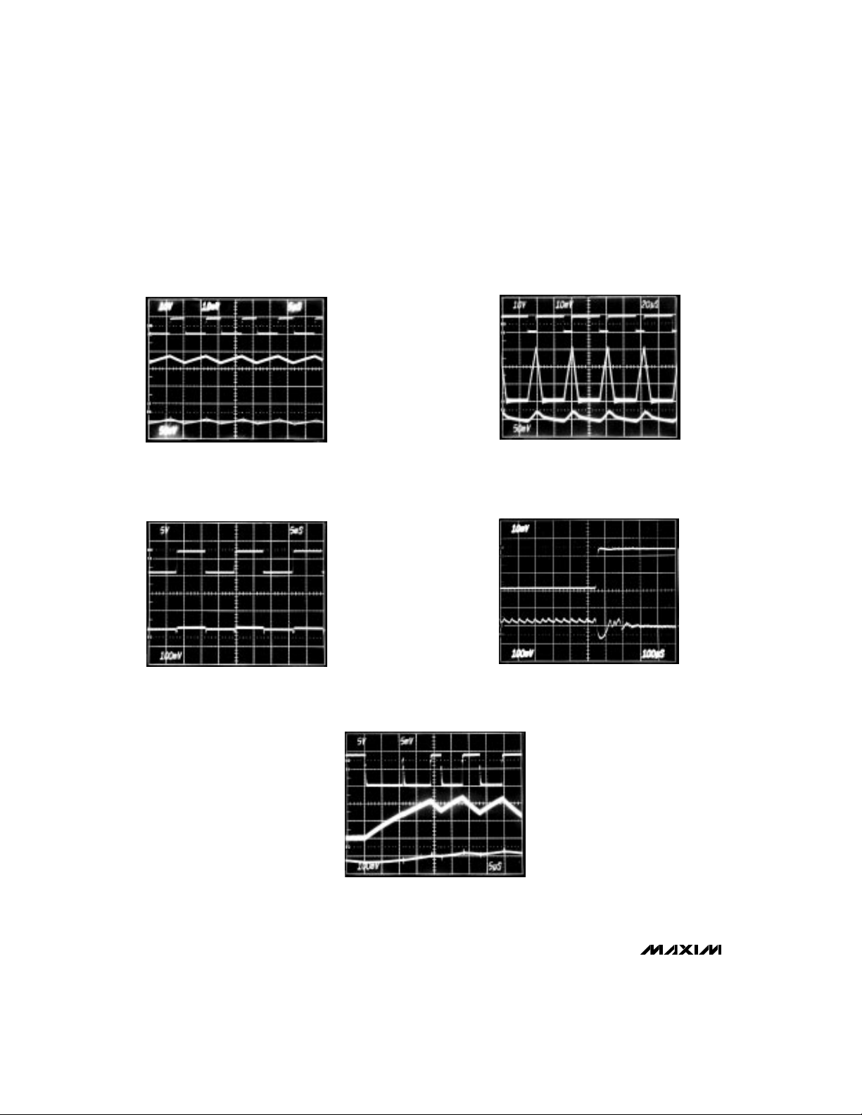
____________________________Typical Operating Characteristics (continued)
CONTINUOUS-CONDUCTION MODE WAVEFORMS
DISCONTINUOUS-CONDUCTION IDLE-MODE WAVEFORMS
MAX747-SCOPE1
MAX747
V+ = 9V, I
a) EXT VOLTAGE, 10V/div
b) INDUCTOR CURRENT, 1A/div
c) V
MAX747-SCOPE4
I
a) V+ = 6V to 12V, 5V/div
b) V
= 2.5A
OUT
RIPPLE, 50mV/div
OUT
LINE-TRANSIENT RESPONSE
= 2.0A
OUT
RIPPLE, 100mV/div
OUT
5µs/div
5ms/div
a
b
c
a
b
MODERATE LOAD, IDLE-MODE WAVEFORMS
MAX747-SCOPE2
20µs/div
V+ = 9V, I
= 125mA
OUT
a) EXT VOLTAGE, 10V/div
b) INDUCTOR CURRENT, 200mA/div
RIPPLE, 50mV/div
c) V
OUT
LOAD-TRANSIENT RESPONSE
MAX747-SCOPE5
100µs/div
V+ = 9V, C
a) LOAD CURRENT, 0.1A TO 2.5A, 1A/div
b) V
= 430µF
OUT
RIPPLE, 100mV/div
OUT
a
b
c
a
b
MAX747-SCOPE3
5µs/div
V+ = 9V, I
a) EXT VOLTAGE, 5V/div
b) INDUCTOR CURRENT, 0.5A/div
c) V
= 560mA
OUT
RIPPLE 100mV/div
OUT
a
b
c
4 _______________________________________________________________________________________
Page 5

High-Efficiency PWM, Step-Down
P-Channel DC-DC Controller
______________________________________________________________Pin Description
PIN NAME FUNCTION
1 LBI Input to the internal low-battery comparator. Tie to V+ or GND if not used.
2 SS
3 REF
4 SHDN
5 FB
6 CC
7 AV+ Quiet supply voltage for sensitive analog circuitry. A bypass capacitor is not required for AV+.
8 OUT
9 CS Negative input to the current-sense amplifier. Connect the current-sense resistor (R
10 AGND Quiet analog ground
11 EXT
12 V+ High-current supply voltage for the output driver
Soft-start limits start-up surge currents. On power-up, it charges the soft-start capacitor, slowly raising the
peak current limit to the level set by the sense resistor.
2V reference output that can source 100µA for external loads. Bypass with 0.22µF. The reference is
disabled in shutdown mode.
Active-high TTL/CMOS logic-level input. In shutdown mode, V
to 20µA.
Feedback input for adjustable-output operation. Connect to GND for fixed +5V output. Use a resistor
divider network to adjust the output voltage. See the section
Compensation capacitor. AC compensation input for the error amplifier. Connect a capacitor between CC
and GND for fixed +5V output operation. See
Output voltage sense input. Connects to internal resistor divider. Leave unconnected for adjustable output.
Bypass to AGND with a 0.1µF capacitor close to the IC.
Power MOSFET gate drive output that swings between V+ and GND. EXT is not protected against short
circuits to V+ or AGND.
Compensation Capacitor
= 0V and the supply current is reduced
OUT
Setting the Output Voltage
section.
.
) from V+ to CS.
SENSE
MAX747
13 GND High-current ground return for the output driver
14 LBO
Low-battery output is an open-drain output that goes low when LBI is less than 2V. Connect to V+ through
a pull-up resistor. Leave floating if not used. LBO is disabled in shutdown mode.
____________________Getting Starting
Figure 1a shows the 5V output 11.4W standard
application circuit and Figure 1b shows the 3.3V output
7.5W standard application circuit. Most applications
will be served by these circuits. To learn more about
component selection for particular applications, refer to
the
Design Procedure
operation of the MAX747, refer to the
Description.
section. To learn more about the
Detailed
_______________________________________________________________________________________ 5
_______________Detailed Description
The MAX747 monolithic, CMOS, step-down switchmode power-supply controller drives external
P-channel FETs. It uses a unique current-mode pulsewidth-modulating (PWM) control scheme that results in
high efficiency over a wide range of load currents, tight
output voltage regulation, excellent load- and linetransient response, and low noise. Efficiency at light
loads is further enhanced by a proprietary Idle-Mode
switching control scheme that skips oscillator cycles in
order to reduce switching losses.
Page 6

High-Efficiency PWM, Step-Down
P-Channel DC-DC Controller
VIN
(7.5V TO15V)
MAX747
R2 R3
R1
C6
470pF
C4
0.1µF
C5
0.22µF
100µF
100k
10
C2
C3
0.1µF
12
7
V+
MAX747
GND
13
AV+
EXT
OUT
R
SENSE
50mΩ
9
CS
Q1
11
SI9405DY
P
L1
8
0.1µF
50µH
430µF
D1
NSQ03A03
C7
430µF
5V
C1
@ 2.3A
C1
14
LBO
1
LBI
6
CC
2
SS
3
REF
5
FB
4
SHDN
AGND
VIN
(4.5V TO 15V)
R2 R3
R1
C4
0.1µF
C5
0.22µF
N.C.
N.C.
100k
C3
C2
0.1µF
100µF
LBO
LBI
OUT
CC
SS
REF
SHDN
AGND
MAX747
12
GND
13
V+
AV+
EXT
14
1
8
6
2
3
4
10
Figure 1b. +3.3V Standard Application CircuitFigure 1a. +5V Standard Application Circuit
Figure 2 is the MAX747 block diagram. The MAX747
Operating Principle
regulates using an inner current-feedback loop and an
outer voltage-feedback loop. The current loop is
that to transfer equal amounts of energy to the load in
one cycle, the peak current level for the discontinuous
waveform must be much larger than the continuous
waveform peak current.
stabilized by a slope compensation scheme and the
voltage loop is stabilized by the dominant pole formed
by the filter output capacitor and the load.
Discontinuous-/Continuous-
Conduction Modes
The MAX747 operates in continuous-conduction mode
(CCM) under heavy loads, but operates in
discontinuous-conduction mode (DCM) at light loads,
making it ideal for variable load applications. In DCM,
the inductor current starts and ends at zero on each
cycle. In CCM, the inductor current never returns to zero.
It is composed of a small AC component superimposed
on a DC level, which results in higher load-current
capability and lower output noise. Output noise is
reduced because the inductor does not exhibit the
ringing that occurs when the inductor current reaches
zero, and because there is a smaller AC component in
the inductor-current waveform (see inductor waveforms
in the
Typical Operating Characteristics
6 _______________________________________________________________________________________
section). Note
Stability of the inner current-feedback loop is provided
by a slope-compensation scheme that adds a ramp
signal to the current-sense amplifier output. Ideal slope
compensation can be achieved by adding a linear
ramp with the same slope as the declining inductor
current to the rising inductor current-sense voltage.
Therefore, the inductor must be scaled to the current-
sense resistor value.
Overcompensation adds a pole to the outer voltage-
feedback loop response that degrades loop stability.
This may cause voltage-mode pulse-frequency-
modulation instead of PWM operation. Under-
compensation results in inner current-feedback loop
instability, and may cause the inductor current to
staircase. Ideal matching between the sense resistor
and inductor is not required. The matching can be
±30% or more.
7
R
SENSE
50mΩ
9
CS
Q1
11
SI9405DY
P
L1
33µH
R5
13k
C1
880µF
@ 2.3A
D1
NSQ03A03
5
FB
R4
C6
20k
2.7nF
Slope Compensation
3.3V
Page 7

High-Efficiency PWM, Step-Down
P-Channel DC-DC Controller
LBO EXT V+
MAX747
OUT
AV+
LBI
LOW-BATTERY
COMPARATOR
REF
60k
CC
40k
DUAL-MODE
FB
100mV
CS
COMPARATOR
N
CURRENT-SENSE
AMPLIFIER
CURRENT-LIMIT
COMPARATOR
+2V
REFERENCE
SLOPE
COMPENSATION
RAMP
ERROR
AMPLIFIER
PWM
COMPARATOR
IDLE-MODE
Σ
V
RAMP
50mV
COMPARATOR
100kHz
OSCILLATOR
EXT
CONTROL
SHDN
SOFT-START
SS
CIRCUITRY
AGND
Figure 2. Block Diagram
The Oscillator and EXT Control
The switching frequency is nominally 100kHz and the
duty cycle varies from 5% to 96%, depending on the
input/output voltage ratio. EXT, which provides the gate
drive for the external P-FET, is switched between V+
and GND at the switching frequency. EXT is controlled
by a unique two-comparator control scheme composed
of a PWM comparator and an idle-mode comparator
_______________________________________________________________________________________ 7
GND
(Figure 2). The PWM comparator determines the cycleby-cycle peak current with heavy loads, and the
light-load comparator sets the light-load peak current.
As V
until both comparators trip. With heavy loads, the idle-
begins to drop, EXT goes low and remains low
OUT
mode comparator trips quickly, and the PWM control
comparator determines the EXT on-time; with light
loads, the idle-mode comparator sets the EXT on-time.
Page 8

High-Efficiency PWM, Step-Down
P-Channel DC-DC Controller
3
MAX747-FIG3
2
V+ –VCS = 150mV
R
= 50mΩ
SENSE
MAX747
1
PEAK CURRENT LIMIT (A)
R
= 100mΩ
0
0
13
SOFT-START VOLTAGE (V)
Figure 3. Peak Current Limit vs. Soft-Start Voltage
With decreasing loads, as the inductor current becomes
discontinuous, traditional PWM converters continue to
switch at a fixed frequency, decreasing light-load efficiency.
However, the MAX747’s idle-mode comparator increases
the peak inductor current, allowing more energy to be
transferred per cycle. Since fewer cycles are required, the
switching frequency is reduced. This keeps the external PFET off for longer periods, minimizing switching losses and
increasing efficiency.
The light-load output noise spectrum widens due to variable
switching frequency in idle-mode, but output ripple remains
low. Using the
Typical Operating Circuit
a 125mA load current, output ripple is less than 40mV.
Soft-Start and Current Limiting
The MAX747 draws its highest current at power-up. If The
power source to the MAX747 cannot provide this initial
elevated current, the circuit may not function correctly. For
example, after prolonged use, a battery’s increased series
resistance may prevent it from providing adequate initial
surge currents when the MAX747 is brought out of
shutdown. Using Soft-Start (SS) minimizes the possibility of
overloading the incoming supply at power-up by gradually
increasing the peak current limit. Connect an external
capacitor from SS to ground to reduce the initial peak
currents drawn from the supply.
The steady-state SS pin voltage is typically 3.8V. On
power-up, SS sources 1µA until the SS voltage reaches
3.8V. The current-limit comparator inhibits EXT switching
until the SS voltage reaches 1.8V. The maximum current
limit is set by:
V
I
PK
LIMIT
==
R
SENSE SENSE
150mV (typ)
SENSE
2
R
4
, with a 9V input and
Figure 3 shows how the peak current limit increases as
the voltage on SS rises for two R
SENSE
values.
Shutdown Mode
When SHDN is high, the MAX747 enters shutdown
mode. In this mode, the internal biasing circuitry
(including EXT) is turned off, V
supply current drops to 0.6µA (20µA max). This
drops to 0V, and the
OUT
excludes external component leakage, which may add
several microamps to the shutdown supply current for
the entire circuit. SHDN is a TTL/CMOS logic-level
input. Connect SHDN to GND for normal operation.
Low-Battery Detector
The MAX747 provides a low-battery comparator that
compares the voltage on LBI to the reference voltage.
LBO, an open-drain output, goes low when the LBI
voltage is below V
as shown in Figure 4 to set the trip voltage (V
the desired level. In this circuit, LBO goes low when
V+ ≤ V
. LBO is high impedance in shutdown mode.
TRIP
. Use a resistor-divider network
REF
TRIP
) to
__________________Design Procedure
The MAX747’s output voltage can be set to 5V by
grounding FB, or adjusted from 2V to 14V using
external resistors R4 and R5, configured as shown in
Figure 5. Select feedback resistor R4 from the 10kΩ to
1MΩ range. R5 is given by:
R5 (R4)
=−
First, approximate the peak current assuming IPKis
(1.1)(I
Once all component values have been determined, the
LOAD
), where I
actual peak current is given by:
I I
=+
PK LOAD
Next, determine the value of R
R
==
SENSE
For example, to obtain 5V at 3A, IPK= 3.3A and R
125mV/3.3A = 38mΩ.
The sense resistor should have a power rating greater
than (I
With a 3A load current, IPK= 3.3A and R
PK
2
)(R
The power dissipated by the resistor (assuming an 80%
Setting the Output Voltage
V
OUT
2V
1
Selecting R
is the maximum load current.
LOAD
(2L) (f )
V
LIMIT (MIN)
I
PK PK
) (with an adequate safety margin).
SENSE
V
OUT
OSC
SENSE
1
−
such that:
125mV
I
V
OUT
V
SENSE
IN
SENSE
SENSE
= 38mΩ.
=
8 _______________________________________________________________________________________
Page 9

High-Efficiency PWM, Step-Down
P-Channel DC-DC Controller
duty cycle) is 331mW. Metal film resistors are
recommended. Do not use wire-wound resistors because
their inductance will adversely affect circuit operation.
Determine the duty cycle for CCM from the following
equation:
Duty cycle (%)
=
V V
+
OUT DIODE
V V V
+− +
SW DIODE
100%
()
where VSWis the voltage drop across the external PFET and sense resistor, and can be approximated as
(I
LOAD
)[R
DS(ON)
+ R
SENSE
].
Inductor Selection
Once the sense resistor value is determined, the
inductor is determined from the following equation. The
value of inductor L ensures proper slope
compensation. Continuing with the above example,
(R ) (V )
SENSE OUT(MAX)
L
=
(V ) (f )
RAMP(MAX) OSC
(38m ) (5V)
=
Ω
(50mV) (100kHz)
38 H
=µ
Although 38µH is the calculated value, the component
used may have a tolerance of ±30% or more. Make
sure the inductor’s saturation current rating (the current
at which the core begins to saturate and the
inductance starts to fall) exceeds the peak current set
by R
SENSE
.
Inductors with molypermalloy powder (MPP), Kool Mµ,
or ferrite are recommended. Inexpensive iron powder
core inductors are not suitable due to their increased
core losses. MPP and Kool Mµ cores have low
permeability, allowing larger currents.
For highest efficiency, use a coil with low DC
resistance. To minimize radiated noise, use a toroid,
pot core, or shielded coil.
External P-FET Selection
To ensure the external P-FET is fully on, use logic-level,
or low threshold P-FETs when the minimum input
voltage is less than 8V.
When selecting the P-FET, three important parameters
to note are total gate charge (Qg), on resistance
(R
), and reverse transfer capacitance (C
DS(ON)
RSS
).
Qg, the total gate charge, includes all capacitances
associated with charging the gate. Use the typical Q
value for best results; the maximum value is usually
overspecified since it is a guaranteed limit and not the
measured value. The typical total gate charge should
be ≤ 50nC. Larger numbers mean that EXT may not be
able to adequately drive the gate. EXT sink/source
capability (I
) is typically 140mA.
EXT
There are two losses associated with the P-FET’s power
dissipation: I2R losses and switching losses. CCM
power dissipation (PD) is approximated by:
2
PD Duty Cycle I R +
=
()
2
V+ C I f
where the duty cycle is approximated by V
100kHz, and R
sheet of the chosen P-FET. In the equation, R
DS(ON)
assumed to be constant, but is actually a function of
PK DS(ON)
[]
()()()
RSS PK OSC
I
EXT
and C
are given in the data
RSS
OUT
/V+, f
DS(ON)
OSC
temperature. Note that the equation does not account
for losses incurred by charging and discharging the
MAX747
g
=
is
V
IN
12
MAX747
V+
LBO
GND
13
R2
1
LBI
R1
Figure 4. Input Voltage Monitor Circuit
_______________________________________________________________________________________ 9
…TO V
OUT
R3
100k
14
R2 = R1 -1
= 2.0V
V
TH
OR VIN
LOW-BATTERY
OUTPUT
V
TRIP
( )
V
TH
VIN
12
V+
5
FB
MAX747
8
N.C.
OUT
GND
13
* SEE
COMPENSATION CAPACITOR
Figure 5. Adjustable Output Circuit
SECTION
C6*
R4
R4 = 10kΩ TO 1MΩ
R5 = R4 -1
( )
R5
...to V
OUT
V
OUT
2V
Page 10

High-Efficiency PWM, Step-Down
P-Channel DC-DC Controller
gate capacitance, because that energy is dissipated
by the gate-drive circuitry, not the P-FET.
The
Standard Application Circuit
an 8-pin Si9405DY surface-mount P-FET that has 0.1Ω
on resistance with a 10V VGS. Optimum efficiency is
obtained when the voltage at the drain swings between
the supply rails (within a few hundred mV).
MAX747
The MAX747’s high switching frequency demands a
high-speed rectifier. Schottky diodes are recommended.
Ensure that the Schottky diode average current rating
exceeds the load current level.
(Figure 1a, 1b) uses
Diode Selection
Capacitor Selection
Output Filter Capacitor
The output filter capacitor C1 should have a low
effective series resistance (ESR), and its capacitance
should remain fairly constant over temperature. This is
especially true when in CCM, since the output filter
capacitor and the load form the dominant pole that
stabilizes the loop. 430µF is adequate for load currents
up to 2.3A in Figure 1a. At low input/output
differentials, it may be necessary to use much larger
output filter capacitors to maintain adequate loadtransient response. See the
Input/Output Differentials
Sprague 595D surface-mount solid tantalum capacitors
and Sanyo OS-CON through-hole capacitors are
recommended due to their extremely low ESR. OS-CON
capacitors are particularly useful at low temperatures.
For best results when using other capacitors, increase
the output filter capacitor’s size or use capacitors in
parallel to reduce ESR.
AC Stability with Low
section.
Input Bypass Capacitor
The input bypass capacitor C2 reduces peak currents
drawn from the voltage source, and also reduces noise
at the voltage source caused by the MAX747’s fast
switching action (this is especially important when other
circuitry is operated from the same source). The input
capacitor ripple current rating must exceed the RMS
input current.
I RMS AC input current
=
RMS
V(V V)
OUT IN OUT
I
=
LOAD
For load currents up to 2.5A, 100µF (C2) in parallel with
a 0.1µF (C3) is adequate. Smaller bypass capacitors
may be acceptable for lighter loads. The input voltage
source impedance determines the capacitor size
V
IN
−
required at the V+ input. As with the output filter
capacitor, a low-ESR capacitor (Sanyo OS-CON,
Sprague 595D, or equivalent) is recommended for
input bypassing.
Soft-Start and Reference Capacitors
A typical value for the soft-start capacitor C4 is 0.1µF,
which provides a 380ms ramp to full current limit. Use
values in the 0.001µF and 1µF range. The nominal time
for C4 to reach its steady-state value is given by:
t (sec) (C4) (3.8 10 )
SS
Note that tSSdoes not equal the time it takes for the
MAX747 to power up, although it does affect start-up
time. Start-up time is also a function of the input voltage
and load current. With a 2.5A load current, a 7V input
voltage, and a 0.1µF soft-start capacitor, power-up
takes typically 360ms.
Bypass REF with a 0.22µF capacitor (C5).
=×
6
Compensation Capacitor
With a fixed +5V output, connect the compensation
capacitor (C6) between CC and GND to optimize
transient response. Appropriate compensation is
determined by the ESR of the output filter capacitor
(C1) and the feedback voltage-sense resistor network.
270pF is adequate for applications where V+ ≤ 9V.
Over the full input voltage range, increase C6 to 470pF.
C6 also depends on the load current, so for light loads,
C6’s value can be reduced. If appropriate
compensation is not obtained using 470pF, use the
following equations to determine C6:
For fixed 5V output operation,
(C1) (ESR )
C6
=
For adjustable-output operation, FB becomes the
compensation input pin and CC is left unconnected.
Connect C6 between FB and GND in parallel with R4
(Figure 5). C6 is determined by:
(C1) (ESR )
C6
=
For example, with a fixed 5V output, C1 = 330µF and
an ESRC1of 0.04Ω (at a 100kHz frequency),
(C1) (ESR )
C6
=
Ω
24k
R4 II R5
Ω
24k
C1
C1
C1
=
783pF
10 ______________________________________________________________________________________
Page 11

High-Efficiency PWM, Step-Down
P-Channel DC-DC Controller
Setting the Low-Battery Detector Voltage
Select R1 between 10kΩ and 1MΩ.
R2 R1
=
(V V
TRIP REF
V
REF
−
)
Connect a pull-up resistor (e.g., 100kΩ) between LBO
and V
(Figure 4).
OUT
__________Applications Information
Due to high current levels and fast switching
waveforms, which radiate noise, proper MAX747 PC
board layout is essential. Protect sensitive analog
grounds by using a star ground configuration. Use an
adequate ground plane and minimize ground noise by
connecting GND, the anode of the steering Schottky
diode, the input bypass capacitor ground lead, and the
output filter capacitor ground lead to a single point
(star ground configuration). Also, minimize lead lengths
to minimize stray capacitance, trace resistance, and
radiated noise. Place bypass capacitor C3 as close as
possible to V+ and GND.
AV+ and CS are the inputs to the differential-input
current-sense amplifier. Use a Kelvin connection
across the sense resistor as shown in Figure 6. Note
that even though AV+ also functions as the supply
voltage for sensitive analog circuitry, a separate AV+
bypass capacitor should not be used. By not using a
capacitor, any noise appearing at the CS input will also
appear at the AV+ input and will appear as a commonmode signal to the current-sense amplifier. A separate
AV+ capacitor causes the noise to appear only on one
input, and this differential noise will be amplified,
adversely affecting circuit operation.
Similarly, CC (or FB in adjustable-output operation) is a
sensitive input that should not be shorted to any node.
Avoid shorting CC when probing the circuit, as this
may damage the device.
A region exists between CCM and DCM where the
inductor current operates in both modes, as shown in
the Idle-Mode Moderate current EXT waveform in the
Typical Operating Characteristics
voltage varies, it is fed back into CC and the duty cycle
is adjusted to compensate for this change. The switch
is considered off when V
threshold voltage. Once the switch is off, the voltage at
EXT is pulled to V+ and the P-FET drain voltage is a
Schottky diode drop below GND. However, in this “in-
Layout Considerations
Switching Waveforms
. As the output
≤ the P-FET’s V
EXT
GS
V
IN
V+
AV+
P
KELVIN SENSE
CONNECTION
L1
V
OUT
R
SENSE
MAX747
Figure 6. Kelvin Connection for Current-Sense Amplifier
CS
EXT
between” mode (due to the changing duty cycle
inherent with DCM), when the device is at maximum
duty cycle, EXT turns off at V+ - V
always pulled to V+ because the switch sometimes
. But it is not
GS
turns on again after a minimum off-time before EXT can
be pulled to V+. The result is short spikes that appear
on the EXT waveform in the
Typical Operating
Characteristics.
AC Stability with Low
Input/Output Differentials
At low input/output differentials, the inductor current
cannot slew quickly to respond to load changes, so the
output filter capacitor must hold up the voltage as the
load transient is applied. In Figure 1a’s circuit, for
V+ = 6.5V, increase the output filter capacitor to 700µF
(Sprague 595D low-ESR capacitors) to obtain a
transient response less than 250mV with a load step
from 200mA to 2.5A. For V+ = 6V and V
increase the output filter capacitor to approximately
OUT
= 5V,
1000µF. As V+ increases, the device will no longer be
operating near full duty cycle with light loads, allowing
it to adjust to full duty cycle when the load transient is
applied and, in turn, allowing smaller output filter
capacitors to be used.
Dual-Mode Operation
The MAX747 is designed in either fixed-output mode
(5V-output, FB = GND) or in adjustable mode (FB = 2V)
using a resistor divider. It is not designed to be
switched from one mode to another when powered up;
however, in adjustment mode, switching between two
different resistor dividers is acceptable.
MAX747
______________________________________________________________________________________ 11
Page 12

High-Efficiency PWM, Step-Down
P-Channel DC-DC Controller
When probing the MAX747 circuit, avoid shorting AV+
Additional Notes
to GND (the two pins are adjacent to each other) as
this may cause the IC to malfunction due to large
ground currents. Also, the MAX747 may continue to
operate with AV+ disconnected, but erratic switching
waveforms will appear at EXT. Finally, due to its fast
switching and high drive capability requirements, EXT
MAX747
is a low-impedance point that is not short-circuit
protected. Therefore, do not short EXT to any node
(including AGND and V+, which are adjacent to EXT)
to prevent damaging the device.
Table 1. Component Suppliers
SUPPLIER PHONE FAX
INDUCTORS
Coiltronics (305) 781-8900 (305) 782-4163
Gowanda (716) 532-2234 (716) 532-2702
Sumida USA (708) 956-0666 (708) 956-0702
Sumida Japan 81-3-3607-511 81-3-3607-5428
CAPACITORS
Kemet (803) 963-6300 (803) 963-6322
Matsuo (714) 969-2491 (714) 960-6492
Nichicon (708) 843-7500 (708) 843-2798
Sprague (603) 224-1961 (603) 224-1430
Sanyo USA (619) 661-6322
Sanyo Japan 81-3-3837-6242
United Chemi-Con (714) 255-9500 (714) 255-9400
DIODES
Motorola (800) 521-6274
Nihon USA (805) 867-2555 (805) 867-2698
Nihon Japan 81-3-3494-7411 81-3-3494-7414
POWER TRANSISTORS
Harris (407) 724-3739 (407) 724-3937
International Rectifier (213) 772-2000 (213) 772-9028
Siliconix (408) 988-8000 (408) 727-5414
RESISTORS
IRC (512) 992-7900 (512) 992-3377
___________________Chip Topography
MAX747
LBI
LBO GND
SS
V+
REF
SHDN
FB
0.080"
(2.03mm)
SUBSTRATE CONNECTED TO V+;
TRANSISTOR COUNT: 508.
AV+
CS
OUT CC
EXT
0.130"
(3.30mm)
AGND
Maxim cannot assume responsibility for use of any circuitry other than circuitry entirely embodied in a Maxim product. No circuit patent licenses are
implied. Maxim reserves the right to change the circuitry and specifications without notice at any time.
12
__________________Maxim Integrated Products, 120 San Gabriel Drive, Sunnyvale, CA 94086 (408) 737-7600
© 1993 Maxim Integrated Products Printed USA is a registered trademark of Maxim Integrated Products.
 Loading...