

Page 1
General Description
The MAX7462/MAX7463 single-channel, standard-definition, integrated video reconstruction filters and buffers
are ideal for anti-aliasing and digital-to-analog smoothing
video applications or wherever analog video is reconstructed from digital data (such as cable/satellite/terrestrial set-top boxes and DVRs).
The MAX7462 includes a disable function, which
places the output in a high-impedance state allowing
multiplexing of multiple output signals. It also has an
external gain control that sets the output buffer gain to
either +6dB or +9.5dB. The higher gain setting allows a
lower DAC output signal than the standard 1V
P-P
signal. The MAX7463 output buffer has a fixed gain of
+6dB.
The MAX7462/MAX7463 operate from a single +5V
supply and have a flat passband out to 5MHz with a
stopband attenuation of -43dB (typ) at 27MHz.
These devices can drive two standard 150Ω AC-coupled or DC-coupled video loads. The output black level
of the MAX7462/MAX7463 is less than 1V for DC-coupled outputs.
The MAX7462 is available in an 8-pin µMAX
®
package
and an 8-pin SO package. The MAX7463 is available in
an 8-pin SO package. All devices are specified over
the 0°C to +85°C temperature range.
Applications
Cable/Satellite/Terrestrial Set-Top Boxes
DVRs
Hard-Disk Recorders
Features
♦ Standard-Definition CVBS Video Reconstruction
Filters and Buffers
♦ Passband: -0.05dB at 5MHz
♦ Stopband: -43dB at 27MHz
♦ Selectable Gain: +6dB and +9.5dB (MAX7462)
♦ Output Disable (MAX7462)
♦ Drives 2V
P-P
into Two 150Ω Video Loads
♦ Output Black Level < 1V for DC-Coupled Output
♦ Very Small µMAX and SO Packages
MAX7462/MAX7463
Single-Channel Video Reconstruction Filters
and Buffers
________________________________________________________________ Maxim Integrated Products 1
19-3790; Rev 0; 8/05
For pricing, delivery, and ordering information, please contact Maxim/Dallas Direct! at
1-888-629-4642, or visit Maxim’s website at www.maxim-ic.com.
Ordering Information
Note: All parts are specified over the 0°C to +85°C temperature
range.
*Future product—contact factory for availability.
µMax is a registered trademark of Maxim Integrated Products, Inc.
Pin Configurations appear at end of data sheet.
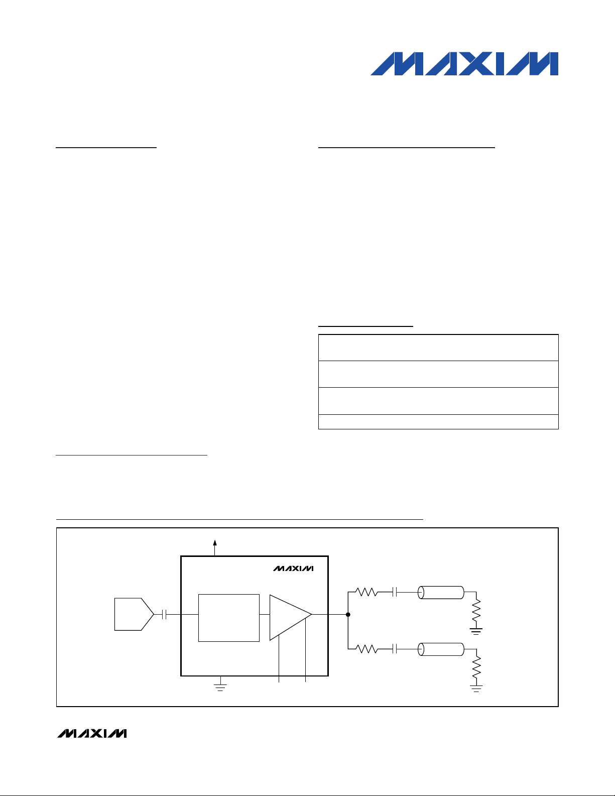
75Ω
75Ω
220µF
220µF
*
*
Z
O
= 75Ω
Z
O
= 75Ω
75Ω
75Ω
OUT
+6dB/+9.5dB
GAIN
DISABLE
GND
LOWPASS
FILTER
V
CC
+5V
DAC
IN
0.1µF
MAX7462
*OPTIONAL
Functional Diagram
PART
MAX7462UUA* 8 µMAX
MAX7462USA* 8 SO
MAX7463USA 8 SO +6 fixed No
PINPACKAGE
BUFFER GAIN
(dB)
+6/+9.5
selectable
+6/+9.5
selectable
OUTPUT
DISABLE
Yes
Yes
Page 2
MAX7462/MAX7463
Single-Channel Video Reconstruction Filters
and Buffers
2 _______________________________________________________________________________________
ABSOLUTE MAXIMUM RATINGS
Stresses beyond those listed under “Absolute Maximum Ratings” may cause permanent damage to the device. These are stress ratings only, and functional
operation of the device at these or any other conditions beyond those indicated in the operational sections of the specifications is not implied. Exposure to
absolute maximum rating conditions for extended periods may affect device reliability.
VCCto GND ........................................................................+6.0V
All Other Pins to GND ...-0.3V to the lower of (V
CC
+ 0.3V) and +6V
Maximum Current into Any Pin Except V
CC
and GND .....±50mA
Continuous Power Dissipation (T
A
= +70°C)
8-Pin µMAX (derate 4.5mW/°C above +70°C) …...... 362mW
8-Pin SO (derate 5.9mW/°C above +70°C) .......... 470.6mW
Operating Temperature Range...............................0°C to +85°C
Storage Temperature Range .............................-65°C to +150°C
Lead Temperature (soldering, 10s) .................................+300°C
ELECTRICAL CHARACTERISTICS
(VCC= +5V ±5%, CL= 0 to 20pF, RL= 75Ω, CIN= 0.1µF, gain = +6dB, DISABLE = VCC(MAX7462), TA=T
MIN
to T
MAX
, unless other-
wise noted. Typical values are at V
CC
= +5V, and TA= +25°C.)
Note 1: Measured after 75Ω back-match resistor. Assume a 75Ω termination resistor.
Passband Response f = 100kHz to 5MHz, relative to 100kHz -0.65 -0.05 +0.65 dB
Stopband Attenuation f ≥ 27MHz 39 43 dB
Output Dynamic Swing Gain = GND (MAX7462) 2.0 2.4 V
Output Sync Tip Clamp Level After termination (Note 1) 0.30 0.45 0.55 V
Group Delay Deviation f = 100kHz to 4.2MHz 11 ns
Differential Gain Five-step modulated staircase 0.15 %
Differential Phase Five-step modulated staircase 0.15 Degrees
Signal-to-Noise Ratio Output signal (2V
Low-Frequency Gain Accuracy f =100kHz, relative to a gain of +6dB -3 +3 %
Line Time Distortion 18µs, 100 IRE bar 0.1 %
Field Time Distortion 130 lines, 18µs, 100 IRE bar 0.1 %
Power-Supply Rejection Ratio VIN = 100mV
Supply Current No load 25 35 mA
PARAMETER CONDITIONS MIN TYP MAX UNITS
P-P
, f = 100kHz 35 dB
P-P
) to RMS noise (100Hz to 5MHz) 75 dB
P-P
Page 3
MAX7462/MAX7463
Single-Channel Video Reconstruction Filters
and Buffers
_______________________________________________________________________________________ 3
Typical Operating Characteristics
(VCC= +5V ±5%, CL= 0 to 20pF, RL= 75Ω, CIN= 0.1µF, gain = +6dB, DISABLE = VCC(MAX7462), TA=T
MIN
to T
MAX
, unless other-
wise noted. Typical values are at V
CC
= +5V, and TA= +25°C.)
0
-20
-40
AMPLITUDE (dB)
-60
NORMALIZED TO 0dB
-80
0.1 100
200
150
100
50
0
-50
PHASE (DEGREES)
-100
-150
-200
0.1 10
AMPLITUDE vs. FREQUENCY
101
FREQUENCY (MHz)
PHASE RESPONSE
vs. FREQUENCY
1
FREQUENCY (MHz)
MAX7462/63 toc01
MAX7462/63 toc03
PASSBAND AMPLITUDE
vs. FREQUENCY
2.0
1.5
1.0
0.5
0
-0.5
AMPLITUDE (dB)
-1.0
-1.5
NORMALIZED TO 0dB
-2.0
0.1 10
1
FREQUENCY (MHz)
GROUP DELAY vs. FREQUENCY
100
90
80
70
GROUP DELAY (ns)
60
50
0.1 10
1
FREQUENCY (MHz)
MAX7462/63 toc02
MAX7462/63 toc04
2T RESPONSE
200ns/div
MAX7462/63 toc05
OUT
250mV/div
IN
250mV/div
MODULATED 12.5T RESPONSE
200ns/div
MAX7462/63 toc06
OUT
250mV/div
IN
250mV/div
Page 4

MAX7462/MAX7463
Single-Channel Video Reconstruction Filters
and Buffers
4 _______________________________________________________________________________________
Typical Operating Characteristics (continued)
(VCC= +5V ±5%, CL= 0 to 20pF, RL= 75Ω, CIN= 0.1µF, gain = +6dB, DISABLE = VCC(MAX7462), TA=T
MIN
to T
MAX
, unless other-
wise noted. Typical values are at V
CC
= +5V, and TA= +25°C.)
2ms/div
OUT RESPONSE TO A FIELD
SQUARE WAVE
OUT
500mV/div
MAX7462/63 toc10
IN
500mV/div
100ns/div
DISABLE TURN-ON TIME
OUT
1V/div
MAX7462/63 toc11
DISABLE
2V/div
GND
GND
100ns/div
OUT
1V/div
MAX7462/63 toc12
DISABLE
2V/div
GND
GND
DISABLE TURN-OFF TIME
10µs/div
MULTIBURST RESPONSE
OUT
250mV/div
MAX7462/63 toc09
IN
250mV/div
10
20
30
40
SUPPLY CURRENT vs. TEMPERATURE
MAX7462/63 toc07
TEMPERATURE (°C)
SUPPLY CURRENT (mA)
01734 85
VIN = +2V
NO LOAD
51 68
DIFFERENTIAL GAIN
MAX7462/63 toc08
DIFFERENTIAL PHASE (deg)
1324567
1324567
0.4
0.6
0.2
0
-0.2
-0.4
-0.6
DIFFERENTIAL GAIN (%)
0.2
0.3
0.1
0
-0.1
-0.2
-0.3
DIFFERENTIAL PHASE
Page 5

Detailed Description
The MAX7462/MAX7463 filters and buffers the analog
CVBS video outputs of DAC video-encoders in applications such as set-top boxes, hard-disk recorders, DVD
players, and digital VCRs. The MAX7462/MAX7463 consist of a lowpass filter and an output video buffer that can
drive two standard 150Ω video loads. These devices
operate from a single +5V supply and have a bandwidth
optimized for interlaced NTSC, PAL, and SDTV.
Filter
The reconstruction filter is a 4th-order Butterworth-type
response that features a maximally flat passband for
NTSC and PAL bandwidths. The stopband attenuation
is optimized for a video-encoder DAC sampling frequency of 27MHz (see the Typical Operating
Characteristics).
Output Buffer
The output buffer can drive two 150Ω video loads with
a 2V
P-P
signal. For the MAX7462, the output buffer gain
is selectable between +6dB and +9.5dB by using GAIN
(see Table 1). The MAX7463 has a fixed gain of +6dB.
The MAX7462/MAX7463 can drive an AC load or drive
the video load directly without using a large output
capacitor. The output buffer can drive DC loads while
maintaining an output blanking level of less than 1V. The
blanking level allows the MAX7462/MAX7463 to meet the
digital TV interface specifications for DC coupling.
Applications Information
Input Considerations
Use a 0.1µF ceramic capacitor to AC-couple the input.
The input capacitor stores a DC voltage so that the output is clamped to the appropriate DC voltage level.
Output Considerations
The outputs are typically connected to a 75Ω series
back-match resistor followed by the video cable.
Because of the inherent divide-by-two of this configuration, the blanking level on the video cable is always
less than 1V, complying with industry-standard video
requirements such as the digital TV standard (which
allows up to 1VDC on the video cable) and the
European SCART standard (which allows up to 2VDC
on the video cable). The video buffer can also drive an
AC-coupled video load. Good video performance is
achieved with an output capacitor as low as 220µF.
Power-Supply Bypassing and Layout
The MAX7462/MAX7463 operate from a single +5V
supply. Bypass V
CC
to GND with a 0.1µF capacitor. In
addition, it is sometimes advantageous to connect a
10µF capacitor within the general vicinity of the video
circuitry. Place all other external components as close
to the device as possible.
MAX7462/MAX7463
Single-Channel Video Reconstruction Filters
and Buffers
_______________________________________________________________________________________ 5
Pin Description
Table 1. Gain Setting Control (MAX7462)
PIN
MAX7462 MAX7463
11IN Video Input. AC-couple IN with a series 0.1µF capacitor.
2—GAIN
3, 4, 5 3 GND Ground
— 2, 4, 5, 6 N.C. No Connection. Not internally connected. Connect to GND for better performance.
6—DISABLE
77VCC+5V Supply Input
88OUT
GAIN BUFFER GAIN (dB)
GND +6
V
CC
NAME FUNCTION
Gain Control Input. Connect GAIN to GND for a gain of +6dB (+2V/V). Connect GAIN to V
for a gain of +9.5dB (+3V/V).
Disable Input. Connect to V
to put the output buffer in a high-impedance state.
Buffer Output. This output can be either AC- or DC-coupled. Use at minimum a 220µF
capacitor for AC-coupled loads.
to enable the output buffer (normal operation). Connect to GND
CC
+9.5
CC
Page 6
MAX7462/MAX7463
Single-Channel Video Reconstruction Filters
and Buffers
6 _______________________________________________________________________________________
Chip Information
PROCESS: BiCMOS
DISABLE
GNDGND
1
2
87OUT
V
CC
GAIN
GND
IN
TOP VIEW
3
4
6
5
MAX7462
N.C.
N.C.N.C.
1
2
87OUT
V
CC
N.C.
GNDIN3
4
6
5
MAX7463
Pin Configurations
Page 7

MAX7462/MAX7463
Single-Channel Video Reconstruction Filters
and Buffers
_______________________________________________________________________________________ 7
Package Information
(The package drawing(s) in this data sheet may not reflect the most current specifications. For the latest package outline information,
go to www.maxim-ic.com/packages
.)
8
Ø0.50±0.1
0.6±0.1
0.6±0.1
1
D
TOP VIEW
A2
E H
A1
4X S
BOTTOM VIEW
A
8
1
DIM
A
A1
A2
b
c
D
e
E
H
L
α
S
INCHES
MIN
-
0.002
0.030
0.010
0.005
0.116
0.0256 BSC
0.116
0.188
0.016
0∞
0.0207 BSC
MAX
0.043
0.006
0.037
0.014
0.007
0.120
0.120
0.198
0.026
6∞
MILLIMETERS
MIN
0.05 0.15
0.25 0.36
0.13 0.18
2.95 3.05
2.95 3.05
4.78
0.41
MAX
- 1.10
0.950.75
0.65 BSC
5.03
0.66
0.5250 BSC
6∞0∞
8LUMAXD.EPS
e
FRONT VIEW
c
b
L
SIDE VIEW
α
PROPRIETARY INFORMATION
TITLE:
PACKAGE OUTLINE, 8L uMAX/uSOP
REV.DOCUMENT CONTROL NO.APPROVAL
21-0036
1
J
1
Page 8

MAX7462/MAX7463
Single-Channel Video Reconstruction Filters
and Buffers
Maxim cannot assume responsibility for use of any circuitry other than circuitry entirely embodied in a Maxim product. No circuit patent licenses are
implied. Maxim reserves the right to change the circuitry and specifications without notice at any time.
8 _____________________Maxim Integrated Products, 120 San Gabriel Drive, Sunnyvale, CA 94086 408-737-7600
© 2005 Maxim Integrated Products Printed USA is a registered trademark of Maxim Integrated Products, Inc.
Boblet
Package Information (continued)
(The package drawing(s) in this data sheet may not reflect the most current specifications. For the latest package outline information,
go to www.maxim-ic.com/packages
.)
N
HE
1
e
TOP VIEW
D
A
B
A1
FRONT VIEW
INCHES
DIM
MIN
0.053A
0.004
A1
0.014
B
0.007
C
e 0.050 BSC 1.27 BSC
0.150
E
H 0.2440.228 5.80 6.20
0.016L
VARIATIONS:
INCHES
MINDIM
D
0.189 0.197 AA5.004.80 8
0.337 0.344 AB8.758.55 14
D
C
L
0∞-8∞
MAX
0.069
0.010
0.019
0.010
0.157
0.050
MAX
0.3940.386D
MILLIMETERS
MAX
MIN
1.35
1.75
0.10
0.25
0.35
0.49
0.19
0.25
3.80 4.00
0.40 1.27
MILLIMETERS
MAX
MIN
9.80 10.00
N MS012
16
AC
SOICN .EPS
SIDE VIEW
PROPRIETARY INFORMATION
TITLE:
PACKAGE OUTLINE, .150" SOIC
REV.DOCUMENT CONTROL NO.APPROVAL
21-0041
1
B
1
 Loading...