

Page 1
19-0192; Rev 1; 11/93
High-Efficiency, PWM, Step-Down,
N-Channel DC-DC Controller
_______________General Description
The MAX746 is a high-efficiency, high-current, step-down
DC-DC power-supply controller that drives external N-channel FETs. It provides 93% to 96% efficiency from a 6V supply
voltage with load currents ranging from 50mA up to 3A. It
uses a pulse-width-modulating (PWM) current-mode control
scheme to provide precise output regulation and low output
noise. The MAX746's 4V to 15V input voltage range, fixed
5V/adjustable (Dual-ModeTM) output, and adjustable current
limit make this device ideal for a wide range of applications.
High efficiency is maintained with light loads due to a proprietary automatic pulse-skipping control (Idle-ModeTM) scheme
that minimizes switching losses by reducing the switching frequency at light loads. The low 950µA quiescent current and
ultra-low 1.4µA shutdown current further extend battery life.
External components are protected by the MAX746's cycleby-cycle current limit. The MAX746 also features a 2V ±1.5%
reference, a comparator for low-battery detection or level
translating, and soft-start and shutdown capability.
The MAX747—discussed in aseparatedata sheet—
functions similarly to the MAX746, but drives P-channel logic
level FETs.
________________________Applications
5V-to-3.3V Green PC Applications
Notebook/Laptop Computers
Personal Digital Assistants
Battery-Operated Equipment
Cellular Phones
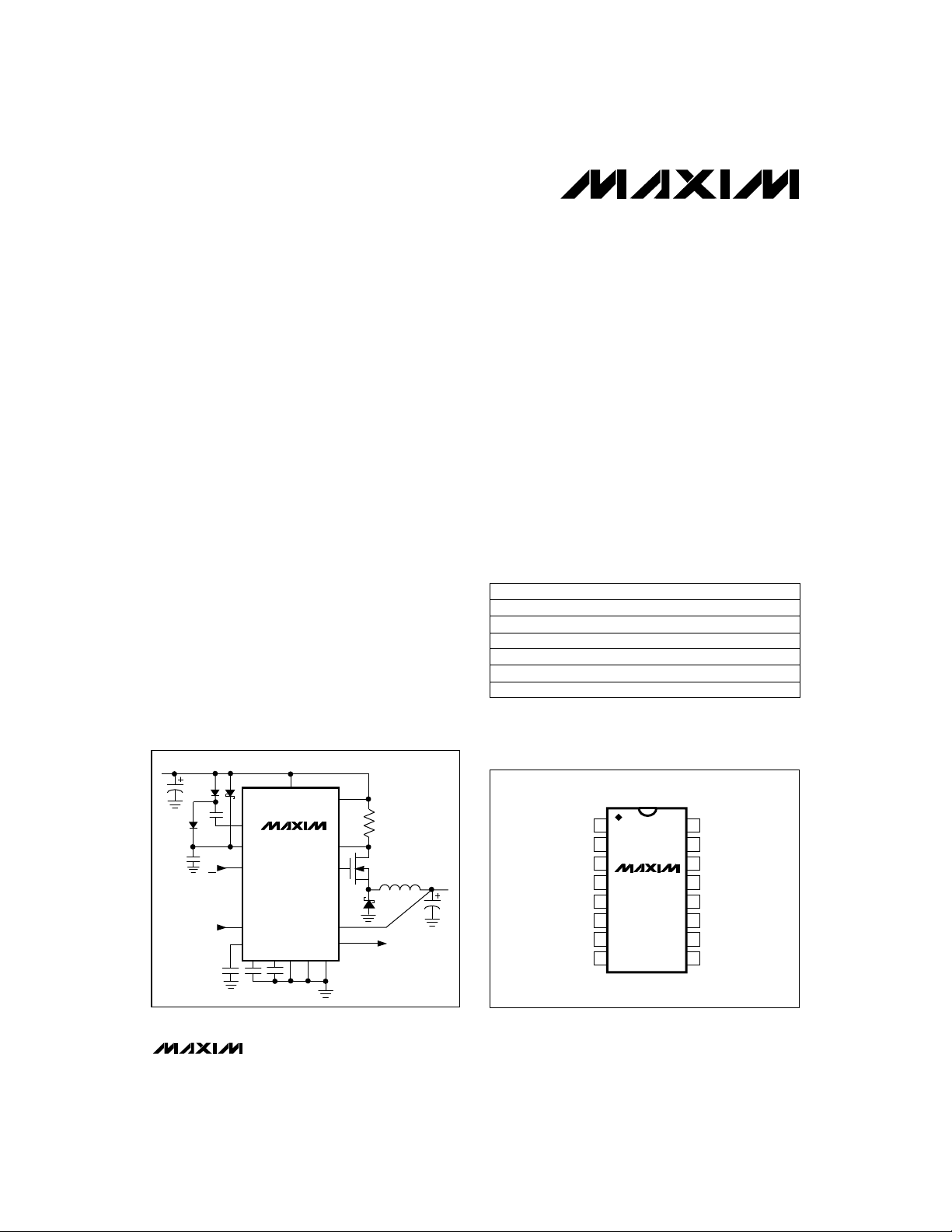
__________Typical Operating Circuit
INPUT 6V TO 15V
V+
AV+
40mΩ
OUTPUT
39µH
440µF
LOW-BATTERY
DETECTOR OUTPUT
5V
ON/OFF
LOW-BATTERY
DETECTOR INPUT
CP
HIGH
SHDN
LBI
REF
SS
MAX746
CC
FB
AGND
GND
CS
EXT
OUT
LBO
____________________________Features
♦ 93% to 96% Efficiency for 50mA to 3A
Output Currents
♦ 4V to 15V Input Voltage Range
♦ Low 950µA Supply Current
♦ 1.4µA Shutdown Current
♦ Drives External N-Channel FETs
♦ Fixed-Frequency Current-Mode PWM (Heavy Loads)
♦ Idle-Mode PFM (Light Loads)
♦ Cycle-by-Cycle Current Limiting
♦ 2V ±1.5% Accurate Reference Output
♦ Adjustable Soft-Start
♦ Undervoltage Lockout
♦ Precision Comparator for Power-Fail or
Low-Battery Warning
______________Ordering Information
PART TEMP. RANGE PIN-PACKAGE
MAX746CPE 0°C to +70°C 16 Plastic DIP
MAX746CSE 0°C to +70°C 16 Narrow SO
MAX746C/D 0°C to +70°C Dice*
MAX746EPE -40°C to +85°C 16 Plastic DIP
MAX746ESE -40°C to +85°C 16 Narrow SO
MAX746MJE -55°C to +125°C 16 CERDIP
* Contact factory for dice specifications.
__________________Pin Configuration
TOP VIEW
LBO
REF
SHDN
AV+
1
LBI
2
SS
3
MAX746
4
5
FB
6
CC
7
8
GND
16
V+
15
CP
14
HIGH
13
EXT
12
AGND
11
CS
10
OUT
9
MAX746
DIP/SO
™Dual-Mode and Idle-Mode are trademarks of Maxim Integrated Products.
________________________________________________________________
Maxim Integrated Products
Call toll free 1-800-998-8800 for free samples or literature.
1
Page 2
High-Efficiency, PWM, Step-Down,
N-Channel DC-DC Controller
ABSOLUTE MAXIMUM RATINGS
Supply Voltage V+, AV+ to GND..............................-0.3V to 17V
HIGH, EXT to GND....................................................-0.3V to 21V
AGND to GND..........................................................-0.3V to 0.3V
All Other Pins................................................-0.3V to (V+ + 0.3V)
Reference Current (I
Continuous Power Dissipation (T
Plastic DIP (derate 10.53mW/°C above +70°C) ..........842mW
MAX746
Narrow SO (derate 8.70mW/°C above +70°C) ............696mW
CERDIP (derate 10.00mW/°C above +70°C)...............800mW
Stresses beyond those listed under “Absolute Maximum Ratings” may cause permanent damage to the device. These are stress ratings only, and functional
operation of the device at these or any other conditions beyond those indicated in the operational sections of the specifications is not implied. Exposure to
absolute maximum rating conditions for extended periods may affect device reliability.
)....................................................±2mA
REF
= +70°C)
A
ELECTRICAL CHARACTERISTICS
(V+ = 10V, I
Input Voltage 415V
Output Voltage
Feedback Voltage V
Line Regulation
Load Regulation 1.3 2.5 %
Efficiency 94 %
OUT Leakage Current 50 80
FB Input Logic Low 40 mV
FB Input Leakage Current 1 100 nAFB = 2V
Reference Voltage V
Reference Load Regulation 920mV
Soft-Start Source Current 0.5 1.0 1.5
Soft-Start Fault Current (Note 1) 100 500
Supply Current (Note 2) I
Oscillator Frequency f
= 0A, I
LOAD
PARAMETER SYMBOL MIN TYP MAX UNITS
= 0µA, TA= T
REF
to T
MIN
V+
V
OUT
FB
REF
SUPP
OSC
, unless otherwise noted.)
MAX
V+ = 6V to 15V, 0V < (V+ - CS) < 0.125V,
FB = 0V (includes line and load regulation)
(V+ - CS) = 0V,
external feedback mode
V+ = 6V to 15V, FB = 0V 0.05
V+ = 4V to 15V, external feedback mode
0V < (V+ - CS) < 0.125V
Circuit of Figure 1, I
V+ = 6V
V
= 5V
OUT
For dual-mode switchover
I
= 0µA
REF
I
= 0µA to 100µA
REF
SS = 0V
SS = 2V
Operating, V+ = 15V
Operating, V+ = 10V
Shutdown mode
Operating Temperature Ranges:
MAX746C_E........................................................0°C to +70°C
MAX746E_E.....................................................-40°C to +85°C
MAX746MJE ..................................................-55°C to +125°C
Junction Temperatures:
MAX746C_E/E_E..........................................................+150°C
MAX746MJE.................................................................+175°C
Storage Temperature Range.............................-65°C to +160°C
Lead Temperature (soldering, 10sec).............................+300°C
CONDITIONS
4.85 5.08 5.25 V
MAX746C 1.96 2.00 2.04
MAX746E/M 1.95 2.00 2.05
0.1
= 0.5A to 2.5A,
LOAD
MAX746C
MAX746E/M
MAX746C 1.1 1.4
MAX746E/M
MAX746E/M
1.97 2.00 2.03
1.96 2.00 2.04
1.7
0.95
1.4 20
85 100 115MAX746C
80 100 120
V
%/V
µA
V
µA
µA
mA
µA
kHz
2 _______________________________________________________________________________________
Page 3
High-Efficiency, PWM, Step-Down,
N-Channel DC-DC Controller
ELECTRICAL CHARACTERISTICS (continued)
(V+ = 10V, I
Maximum Duty Cycle 91 96 %
Charge-Pump Output Voltage
Current-Sense Amplifier
Current-Limit Threshold
EXT Output High V
EXT Output Low
EXT Sink Current 160 mA
EXT Source Current 270 mA
Compensation Pin Impedance 24
LBI Threshold Voltage
LBO Output Voltage Low V
LBI Input Leakage Current nA
LBO Output Leakage Current 1
SHDN Input Voltage Low V
SHDN Input Voltage High V
SHDN Input Leakage Current
Note 1: The soft-start fault current is the current sink capability of SS when V
Note 2: I
= 0A, I
LOAD
PARAMETER
is the supply current drawn by V+, which includes the current drawn by the charge pump. The charge pump
SUPP
doubles the current drawn by HIGH from the V+ input, so I
= 0µA, TA= T
REF
to T
MIN
SYMBOL MIN TYP MAX UNITS
V
HIGH
V
LIMIT
OL
IL
IH
, unless otherwise noted.)
MAX
CONDITIONS
V+ = 6V
I
= 0mA to 10mA
HIGH
V+ – CS
V
forced to 15V, I
HIGH
V
forced to 15V, I
HIGH
V
= 15V, V
HIGH
V
HIGH
LBI falling
I
= 0.5mA
SINK
LBI = 2.5V
V+ = 15V, LBO = 15V, LBI = 2.5V
SHDN = 10V
= 15V, V
EXT
EXT
EXT
EXT
= 12.5V
= 2.5V
SUPP
= -1mA
= 1mA
REF
= IV++ 2I
V+ + 4 V+ + 5 V+ + 6 V
125 150 175 mV
- 0.1 V
HIGH
MAX746C 1.97 2.00 2.03
MAX746E/M
< 1V or when the device is in shutdown.
HIGH
1.96 2.00 2.04
2.0 V
0.1 100
.
0.25 V
0.4 V
100
0.4 V
MAX746
kΩ
V
µA
nA
_______________________________________________________________________________________ 3
Page 4
High-Efficiency, PWM, Step-Down,
N-Channel DC-DC Controller
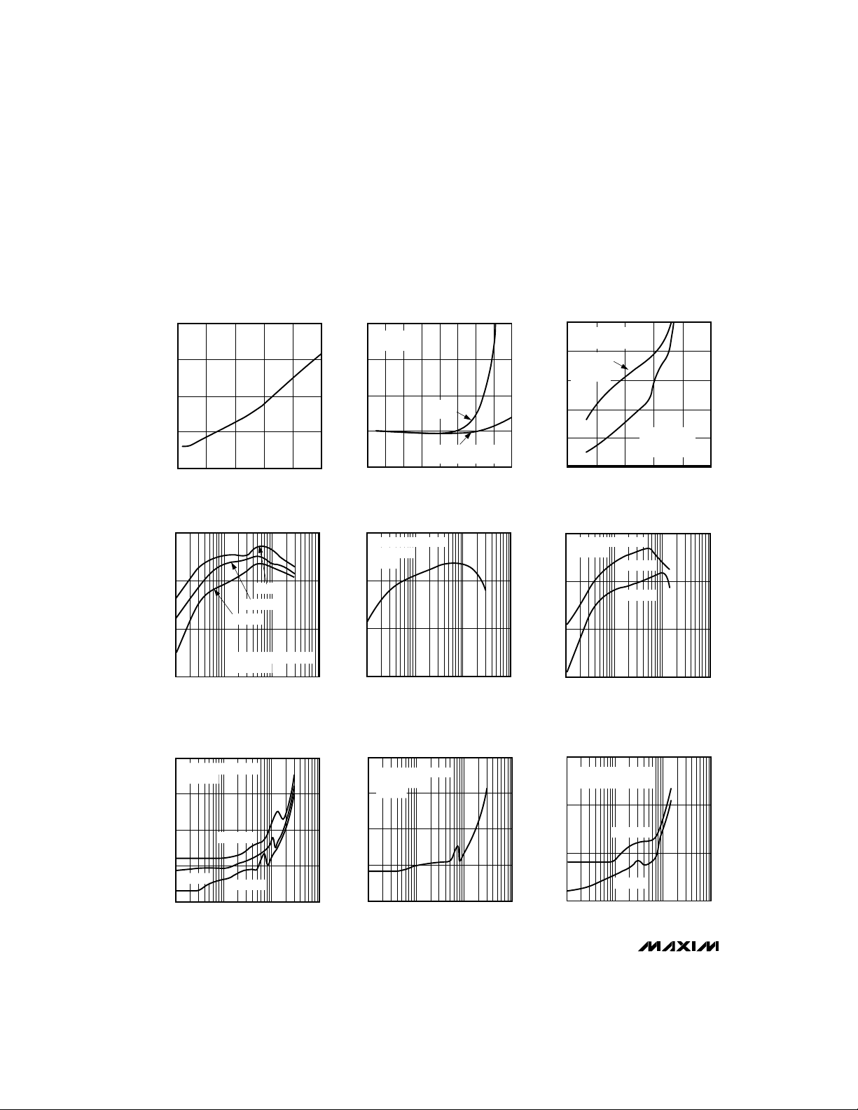
__________________________________________Typical Operating Characteristics
(Circuit of Figure 1a, TA = +25°C, unless otherwise noted.)
N0-LOAD SUPPLY CURRENT
1.2
MAX746
1.1
1.0
0.9
NO-LOAD SUPPLY CURRENT (mA)
0.8
579111315
EFFICIENCY vs. OUTPUT CURRENT
100
90
EFFICIENCY (%)
80
vs. SUPPLY VOLTAGE
SUPPLY VOLTAGE (V)
VIN = 6V
VIN = 9V
VIN = 12V
4
MAX746-01
3
2
1
NO-LOAD SUPPLY CURRENT (mA)
0
-75
100
MAX746-07
CIRCUIT OF FIGURE 1b
V
V+ = 5V
90
EFFICIENCY (%)
80
NO-LOAD SUPPLY CURRENT
V+ = 9V
= 5V
V
OUT
-50 -25 0 25 50 75 100 125
EFFICIENCY vs. OUTPUT CURRENT
= 3.3V
OUT
vs. TEMPERATURE
ENTIRE
CIRCUIT
SCHOTTKY DIODE
LEAKAGE EXCLUDED
TEMPERATURE (°C)
MAX746-02
MAX746-08
CONTINUOUS-CONDUCTION MODE
BOUNDARY AND CORRESPONDING
PEAK INDUCTOR CURRENT
15
DISCONTINUOUS-
CONDUCTION REGION
13
PEAK
INDUCTOR
CURRENT
11
9
SUPPLY VOLTAGE (V)
7
5
0.9 1.1 1.3 1.5 1.7
0.7
OUTPUT CURRENT (A)
EFFICIENCY vs. OUTPUT CURRENT
100
CIRCUIT OF FIGURE 1c
V
= 5V
OUT
90
EFFICIENCY (%)
80
VIN = 6V
VIN = 12V
CONTINUOUS-
CONDUCTION
REGION
MAX746-09
MAX746-06
CIRCUIT OF FIGURE 1a
= 5V
V
70
0.01
4
CIRCUIT OF FIGURE 1a
V
3
2
1
PEAK INDUCTOR CURRENT (A)
VIN = 9V
0
0.01
OUT
0.1 1 10
OUTPUT CURRENT (A)
PEAK INDUCTOR CURRENT
vs. OUTPUT CURRENT
= 5V
OUT
VIN = 12V
VIN = 6V
0.1 1 10
OUTPUT CURRENT (A)
70
0.01
4
MAX746-03
CIRCUIT OF FIGURE 1b
V
OUT
3
V+ = 5V
2
1
PEAK INDUCTOR CURRENT (A)
0
0.01
0.1 1 10
OUTPUT CURRENT (A)
PEAK INDUCTOR CURRENT
vs. OUTPUT CURRENT
= 3.3V
0.1 1 10
OUTPUT CURRENT (A)
MAX746-05
PEAK INDUCTOR CURRENT (A)
70
0.01
1.5
1.0
0.5
0
0.01
0.1 1 10
OUTPUT CURRENT (A)
PEAK INDUCTOR CURRENT
vs. OUTPUT CURRENT
CIRCUIT OF FIGURE 1c
V
= 5V
OUT
VIN = 12V
VIN = 6V
0.1 1
OUTPUT CURRENT (A)
4 _______________________________________________________________________________________
MAX746-03
10
Page 5
High-Efficiency, PWM, Step-Down,
N-Channel DC-DC Controller
____________________________Typical Operating Characteristics (continued)
(Circuit of Figure 1a, TA = +25°C, unless otherwise noted.)
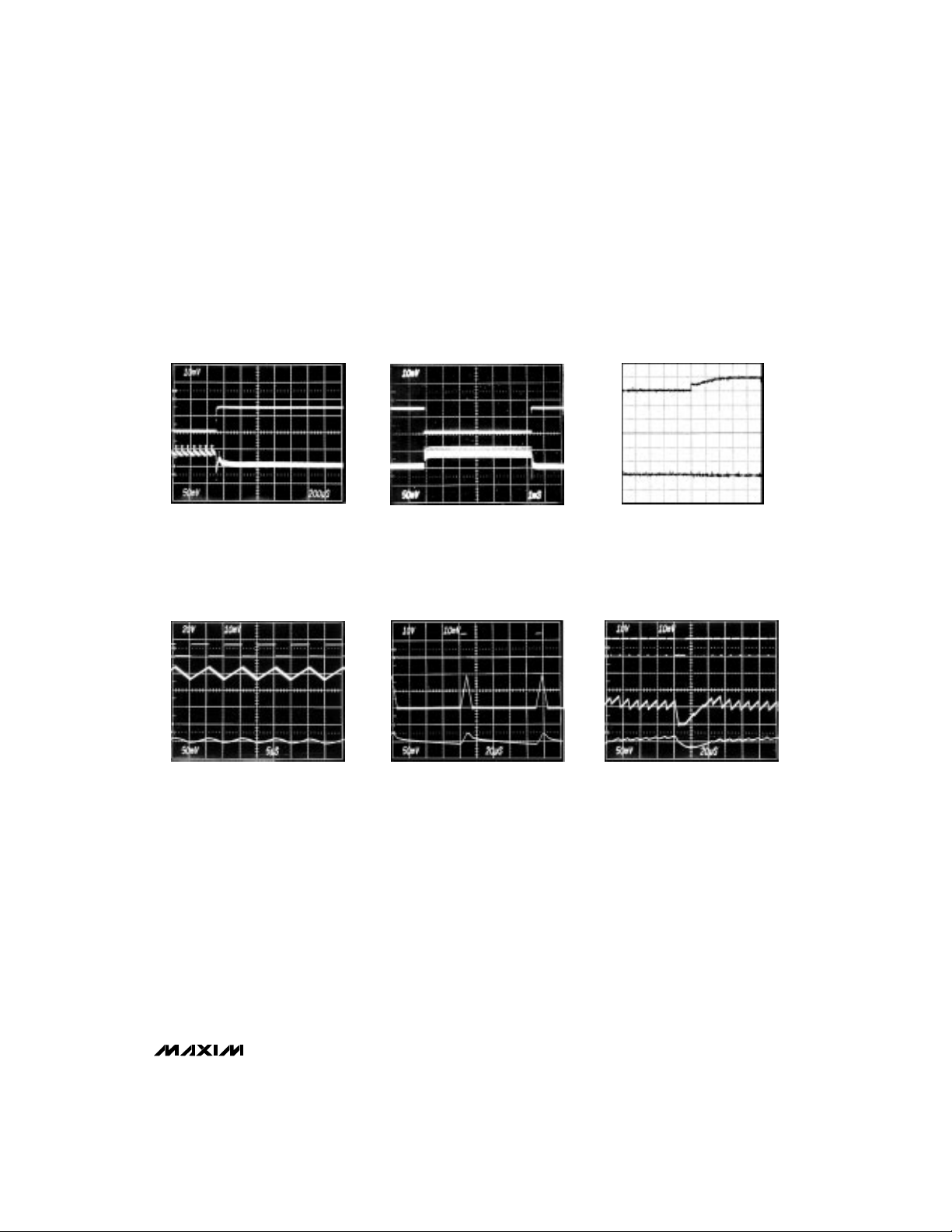
LOAD-TRANSIENT RESPONSE
200µs/div
A: LOAD CURRENT, 0.1A TO 1.5A, 1A/div
B: V
RIPPLE, 50mV/div, AC-COUPLED
OUT
V+ = 10V
CONTINUOUS-CONDUCTION MODE
WAVEFORMS
LOAD-TRANSIENT RESPONSE
A
B
A: LOAD CURRENT, 0.1A TO 1.5A, 1A/div
B: V
RIPPLE, 50mV/div, AC COUPLED
OUT
V+ = 10V
DISCONTINUOUS-CONDUCTION
IDLE-MODE WAVEFORMS
A
B
0V
C
A
B
1ms/div
A
B
C
LINE-TRANSIENT RESPONSE
8V
500ms/div
A: V+ = 8V TO 10V, 2V/div
RIPPLE, 100mV/div
B: V
OUT
I
= 3A
OUT
MODERATE-LOAD, IDLE-MODE
WAVEFORMS
10V
A
B
MAX746
A
B
C
5µs/div
A : EXT VOLTAGE, 20V/div
B : INDUCTOR CURRENT 1A/div
C : V
RIPPLE, 50mV/div
OUT
V+ = 10V, I
= 3A
OUT
_______________________________________________________________________________________
20µs/div
A: EXT VOLTAGE, 10V/div
B: INDUCTOR CURRENT, 500mA/div
C: V
RIPPLE, 50mV/div, AC-COUPLED
OUT
V+ = 10V, I
OUT
= 75mA
20µs/div
A: EXT VOLTAGE, 10V/div
B: INDUCTOR CURRENT, 500mA/div
C: V
RIPPLE, 50mV/div, AC-COUPLED
OUT
V+ = 6V, I
= 480mA
OUT
5
Page 6

High-Efficiency, PWM, Step-Down,
N-Channel DC-DC Controller
______________________________________________________________Pin Description
PIN NAME FUNCTION
1 LBO
2 LBI Input to the low-battery comparator. Tie to V+ or GND if not used.
MAX746
3 SS
4 REF
5 SHDN
6 FB
7 CC
8 AV+
9 OUT
10 CS
11 AGND Quiet analog ground.
12 EXT
13 HIGH Regulated high-side voltage, 5V above the V+ supply voltage.
14 CP Charge-pump output that generates a 0V to V+, 50kHz square wave (see
15 V+ High-current supply voltage for the charge pump.
16 GND High-current ground return for the output driver and charge pump.
Low-battery output is an open-drain output that goes low when LBI is less than 2V. Connect to V+ through a
pull-up resistor. Leave floating if not used. LBO is disabled in shutdown mode.
Soft-start limits start-up surge currents. On power-up, it charges the soft-start capacitor, slowly raising the peak
current limit to the level set by the sense resistor.
2V reference output can source 100µA for external loads. Bypass with 1µF. The reference is disabled in shutdown mode.
Active-high logic input. In shutdown mode, V
Connect to GND for normal operation.
Feedback input for adjustable-output operation. Connect to GND for fixed 5V output. Use a resistor-divider net-
work to adjust the output voltage (see
AC compensation input for the error amplifier. Connect a capacitor between CC and GND for fixed 5V-output
operation (see
Quiet supply voltage for sensitive analog circuitry. Also the noninverting input to the current-sense amplifier. A
separate bypass capacitor is not recommended for AV+.
Output voltage sense that connects to the internal resistor divider. Bypass with 0.1µF to AGND, close to the IC
for fixed output operation. Leave unconnected for adjustable-output operation.
Inverting input to the current-sense amplifier. Connect the current-sense resistor (R
Power MOSFET gate-drive output that swings between HIGH and GND. EXT is not protected against short circuits to V+ or AGND.
Compensation Capacitor
Setting the Output Voltage
= 0V and the supply current is reduced to less than 20µA.
OUT
section).
section).
SENSE
Charge Pump
) from AV+ to CS.
section).
____________________Getting Started
Figure 1a shows the 5V-output 3A standard application
circuit, Figure 1b shows the 3.3V-output 3A standard
application circuit, and Figure 1c shows the 5V-output
1.5A standard application circuit. Most applications will
be served by these circuits. To learn more about component selection for particular applications, refer to the
Design Procedure
ation of the MAX746, refer to the
section. To learn more about the oper-
Detailed Description
.
_______________Detailed Description
The MAX746 monolithic, CMOS, step-down, switchmode power-supply controller provides high-side drive
for external logic-level N-channel FETs. A charge pump
generates a voltage 5V above the supply voltage for
high-side drive capability. The MAX746 uses a unique
6 _______________________________________________________________________________________
current-mode pulse-width-modulating (PWM) control
scheme that results in tight output-voltage regulation,
excellent load- and line-transient response, low noise,
and high efficiency over a wide range of load currents.
Efficiency at light loads is further enhanced by a proprietary idle-mode switching control scheme that skips
oscillator cycles in order to reduce switching losses.
Other features include undervoltage lockout, shutdown,
and a low-battery detection comparator.
Operating Principle
Figure 2 is the MAX746 block diagram. The MAX746
regulates using an inner current-feedback loop and an
outer voltage-feedback loop. A slope-compensation
scheme stabilizes the current loop; the dominant pole,
formed by the output filter capacitor and the load,
stabilizes the voltage loop.
Page 7

High-Efficiency, PWM, Step-Down,
N-Channel DC-DC Controller
VIN
6V TO 15V
C3
0.1µF
R2
R1
0.1µF
1.0µF
SEE TABLE 2 FOR DIODE SELECTION.
*
C2
100µF
15
LBI
SS
REF
FB
SHDN
AGND
V+
MAX746
GND
16
2
C5
3
C6
4
6
5
11
Figure 1a. 5V Standard Application Circuit (15W)
Discontinuous-/Continuous-
Conduction Modes
The MAX746 is designed to operate in continuous-conduction mode (CCM) but can also operate in discontinuous-conduction mode (DCM), making it ideal for variableload applications. In DCM, the current starts at zero and
returns to zero on each cycle. In CCM, the inductor current
never returns to zero; it consists of a small AC component
superimposed on a DC offset. This results in higher current
capability because the AC component in the inductor current waveform is small. It also results in lower output noise,
since the inductor does not exhibit the ringing that would
occur if the current reached zero (see inductor waveforms
in the
Typical Operating Characteristics
). To transfer equal
amounts of energy to the load in one cycle, the peak current level for the discontinuous waveform must be much
larger than the peak current for the continuous waveform.
Slope Compensation
Slope compensation stabilizes the inner current-feedback
loop by adding a ramp signal to the current-sense amplifier
output. Ideal slope compensation can be achieved by
adding a linear ramp, with the same slope as the declining
inductor current, to the rising inductor current-sense voltage.
D3
1N914
Si9410DY
C9
4.7µF
*
Q1
NSQ03A03
R
SENSE
40mΩ
L1
N
39µH
D1
R3
100k
5V
AT 3A
C1
430µF
HIGH
AV+
EXT
OUT
LB0
D4
1N5817
D2
1N914
*
C8
0.1µF
14
CP
13
8
10
CS
12
7
CC
C7
2.7nF
9
C4
0.1µF
1
Under these conditions, the inductor must be scaled to the
current-sense resistor value.
Overcompensation adds a pole to the outer voltage feedback-loop response, degrading loop stability. This may cause
voltage-mode pulse-frequency-modulation instead of PWM
operation. Undercompensation results in inner current feedback-loop instability, and may cause the inductor current to
staircase. Ideal matching between the sense resistor and
inductor is not required; it can differ by ±30% or more.
Oscillator and EXT Control
The oscillator frequency is nominally 100kHz, and the duty
cycle varies from 5% to 96%, depending on the input/output voltage ratio. EXT, which provides the gate drive for the
external logic-level N-FET, is switched between HIGH and
GND at the switching frequency. EXT is controlled by a
unique two-comparator control scheme consisting of a PWM
comparator and an idle-mode comparator (Figure 2). The
PWM comparator determines the cycle-by-cycle peak current with heavy loads, and the idle-mode comparator sets
the light-load peak current. As V
begins to drop, EXT
OUT
goes high and remains high until both comparators trip.
With heavy loads, the idle-mode comparator trips first and
the PWM control comparator determines the EXT on-time;
MAX746
_______________________________________________________________________________________ 7
Page 8

High-Efficiency, PWM, Step-Down,
N-Channel DC-DC Controller
V
IN
4.5V TO 6V
C3
0.1µF
C2
100µF
D2
1N914
D3
1N914
D5
1N914
D6
1N914
D4
1N5817
C11
1µF
R2
MAX746
R1
SUMIDA CDR125 22µH SURFACE-MOUNT INDUCTOR
*
C5
0.1µF
C6
1µF
2
LBI
3
SS
4
REF
5
SHDN
11
AGND
15
V+
MAX746
GND
16
HIGH
AV+
EXT
OUT
LB0
14
CP
13
8
10
CS
12
7
CC
9
6
FB
1
Figure 1b. 3.3V Standard Application Circuit (9.9W)
with light loads, the PWM comparator trips quickly and the
idle-mode comparator sets the EXT on-time.
Traditional PWM converters continue to switch on every
cycle, even when the inductor current is discontinuous
due to smaller loads, decreasing light-load efficiency.
In contrast, the MAX746’s idle-mode comparator increases the switch on-time, allowing more energy to be transferred per cycle. Since fewer cycles are required, the
switching frequency is reduced, resulting in minimal
switching losses and increased efficiency.
The light-load output noise spectrum widens due to the
variable switching frequency in idle-mode, but output
ripple remains low. Using the Typical Operating Circuit,
with a 9V input and a 125mA load current, output ripple
is less than 40mV.
Charge Pump
The MAX746 contains all the control circuitry required
to provide a regulated charge-pump voltage 5V
above V+ for high-side driving N-channel logic FETs.
The charge pump operates with a nominal 50kHz fre-
C8
0.1µF
C7
2nF
C9
C10
1µF
0.1µF
R
SENSE
40mΩ
Q1
R5
13k (1%)
R4
20k (1%)
Si9410DY
NSQ03A03
L1*
N
22µH
D1
R3
100k
C4
0.1µF
quency. When the voltage at HIGH exceeds AV+ by
5V, the charge-pump oscillator is inhibited (Figure 2).
When the voltage at HIGH is less than 4.3V below V+,
undervoltage lockout occurs. Use the voltage tripler
(Figure 3b) when V+ ≤ 6V; otherwise, use the voltage
doubler (Figure 3a).
Soft-Start and Current Limiting
The MAX746 draws its highest current at power-up. If
the power source to the MAX746 cannot provide this
initial elevated current, the circuit may not function correctly. For example, after prolonged use the increased
series resistance of a battery may prevent it from providing adequate initial surge currents when the
MAX746 is brought out of shutdown. Using soft-start
(SS) minimizes the possibility of overloading the incoming supply at power-up by gradually increasing the
peak current limit. Connect an external capacitor from
SS to AGND to reduce the initial peak currents drawn
from the supply.
3.3V
AT 3A
C3
660µF
8 _______________________________________________________________________________________
Page 9

High-Efficiency, PWM, Step-Down,
N-Channel DC-DC Controller
V
IN
6V TO 15V
C3
0.1µF
R2
R1
0.1µF
1µF
SEE TABLE 2 FOR DIODE SELECTION.
*
SUMIDA CDR125 SURFACE-MOUNT INDUCTOR.
**
C2
47µF
2
LBI
C5
3
SS
C6
4
REF
6
FB
5
SHDN
11
AGND
Figure 1c. 5V Standard Application Circuit (7.5W)
V+
MAX746
GND
MAX746
D3
1N914
*
Si9410DY
NSQ03A03
C9
4.7µF
Q1
R
SENSE
75mΩ
L1**
N
82µH
D1
R3
100k
5V
AT 1.5A
C1
220µF
D4
1N5817
HIGH
AV+
EXT
OUT
LB0
D2
1N914
*
C8
0.1µF
14
CP
13
8
10
CS
12
7
CC
C7
1nF
9
C4
0.1µF
1
15
16
The steady-state SS pin voltage is typically 3.8V. On
power-up, SS sources 1µA until its voltage reaches
3.8V. The current-limit comparator inhibits EXT switching until the SS voltage reaches 1.8V. The peak current
limit is set by:
V
where V
LIMIT
_________
IPK=
R
SENSE
is the differential voltage across the current-
LIMIT
150mV (typ)
___________
=
R
SENSE
sense amplifier inputs. Figure 4 shows how the SS peak
current limit increases as the voltage on SS rises for two
R
values.
SENSE
Undervoltage Lockout
Undervoltage lockout inhibits operation of EXT until the
charge pump is capable of generating a voltage greater
than 4.3V above the supply voltage (Figure 2). When
the undervoltage-lockout comparator detects an undervoltage condition, the switching action at EXT is halted.
_______________________________________________________________________________________ 9
When SHDN is high, the MAX746 is shut down. In this
Shutdown Mode
mode, the internal biasing circuitry (including EXT) is
turned off, V
drops to 0V, and the supply current
OUT
drops to 1.4µA (20µA max). This excludes external
component leakage, which may add several
microamps to the shutdown supply current for the
entire circuit. SHDN is a logic input. Connect SHDN to
GND for normal operation.
Low-Battery Detector
The MAX746 provides a low-battery comparator that
compares the voltage on LBI to the reference voltage.
LBO, an open-drain output, goes low when the LBI voltage is below V
. Use a resistor-divider network, as
REF
shown in the Input Voltage Monitor Circuit (Figure 5),
to set the trip voltage (V
this circuit, LBO goes low when V+ ≤ V
) at the desired level. In
TRIP
. LBO is high
TRIP
impedance in shutdown mode.
Page 10

High-Efficiency, PWM, Step-Down,
N-Channel DC-DC Controller
LBI
MAX746
REF
OUT
CC
FB
100mV
AV+
CS
LOW-BATTERY
COMPARATOR
DUAL-MODE
COMPARATOR
CURRENT-SENSE
AMPLIFIER
COMPENSATION
SLOPE-
RAMP
LBO
N
+2V
REFERENCE
V
RAMP
EXT
ERROR
AMPLIFIER
Σ
50mV
HIGH
4.3V
5V
PWM
COMPARATOR
LIGHT-LOAD
COMPARATOR
FROM AV+
CHARGE-PUMP CONTROL
COMPARATOR
UNDERVOLTAGE-
LOCKOUT
COMPARATOR
EXT
CONTROL
T
T FLIP-
FLOP
100kHz
OSCILLATOR
V+ PUMP
Q
SHDN
SOFT-START
SS
CIRCUITRY
CURRENT-LIMIT
COMPARATOR
AGND
GND
Figure 2. Block Diagram
10 ______________________________________________________________________________________
Page 11

High-Efficiency, PWM, Step-Down,
N-Channel DC-DC Controller
V
IN
15
V+
D2
1N914
0.1µF
C8
MAX746
T FLIP-
T
FLOP
CLK
100kHz
OSCILLATOR
GND
MAX746
GND
CP
AV+
HIGH
HIGH
14
13
5V
D3
D2
1N914
1N914
C8
0.1µF
14
CP
13
Q
16
V
IN
15
V+
16
Figure 3. Charge-Pump Configurations
3a. CHARGE-PUMP
VOLTAGE DOUBLER
D4
D3
1N5817
1N914
3b. CHARGE-PUMP
VOLTAGE TRIPLER
D4
1N5817
D5
D6
1N914
1N914
C9
C10
1µF
0.1µF
C9
1µF
C11
1µF
PEAK CURRENT LIMIT
vs. SOFT-START VOLTAGE
3
R
= 50mΩ
SENSE
2
V+ - VCS = 150mV
1
PEAK CURRENT LIMIT (A)
R
= 100mΩ
0
01234
SOFT-START VOLTAGE (V)
SENSE
Figure 4. Peak Current Limit vs. Soft-Start Voltage
V
IN
15
R2
2
R1
V+
MAX746
LBI
GND
16
LBO
…TO V
OUT
R3
100k
1
LOW-BATTERY
R2 = R1 -1
= 2.0V
V
REF
OR VIN
( )
Figure 5. Input Voltage Monitor Circuit
MAX746-FG03
OUTPUT
V
TRIP
V
REF
MAX746
__________________Design Procedure
The MAX746’s dual-mode output voltage can be set
to 5V by grounding FB, or it can be adjusted from
2V to 14V using external resistors R4 and R5 configured as shown in Figure 6. Select feedback resistor
R4 in the 10kΩ to 60kΩ range. R5 is given by:
The MAX746 is designed to use either internal or external feedback mode, but should not be toggled between
Setting the Output Voltage
V
OUT
R5 = (R4)
______________________________________________________________________________________ 11
_______
(
2V
– 1
)
the two modes while operating. If two different output
voltages are required, use external feedback mode
with a resistor network similar to the 3.3V/5V adjustable
output circuit shown in Figure 7.
To select the sense-resistor value (R
Selecting R
SENSE
SENSE
), first
approximate the peak current assuming IPKis
(1.1) (I
LOAD
), where I
is the maximum load cur-
LOAD
rent. Once all component values have been determined, the actual peak current is given by:
IPK= I
LOAD
___________
+
(
(2L) (f
V
OUT
OSC
V
OUT
_______
1–
)(
)V
)
IN
Page 12

High-Efficiency, PWM, Step-Down,
N-Channel DC-DC Controller
VIN
15
V+
MAX746
* SEE
Figure 6. Adjustable Output Circuit
MAX746
GND
16
COMPENSATION CAPACITOR
FB
OUT
SECTION.
6
C7*
9
R5
R4
R4 = 10kΩ TO 60kΩ
V
OUT
R5 = R4 -1
( )
V
REF
= 2.0V NOMINAL
V
REF
V
OUT
SELECT WITH FET OFF:
SELECT WITH FET OFF:
Figure 7. 3.3V/5V Ajustable Output Circuit
MAX746
V
= V
OUT
V
= V
OUT
= 2.0V NOMINAL
V
REF
12
EXT
6
FB
9
OUT
R5
+1
REF
( )
R4a
R5
REF +1
( )
R4a + R4b
5V/3.3V
N
D1
26.1k (1%)
17.4k (1%)
L
R4a
R5
N
V
OUT
C1
C7
R4b
22.6k (1%)
Next, determine the value of R
V
LIMIT(min)
R
SENSE
_____________
=
I
PK
SENSE
such that:
125mV
________
=
I
PK
For example, to obtain 5V at 3A, IPK= 3.3A and
R
= 125mV/3.3A = 38mΩ.
SENSE
The sense resistor should have a power rating greater
PK
2)
(R
) with an adequate safety margin.
SENSE
SENSE
= 38mΩ.
than (I
With a 3A load current, IPK= 3.3A and R
The power dissipated by the resistor (assuming an 80%
duty cycle) is 331mW. Metal-film resistors are recommended. Do not use wire-wound resistors because
their inductance will adversely affect circuit operation.
The duty cycle (for continuous conduction) is determined
from the following equation:
V
V
OUT
DIODE
Duty Cycle (%) =
_____________________
+
V+ - VSW+ V
DIODE
x 100%
where VSWis the voltage drop across the external
N-FET and sense resistor. VSWcan be approximated
as [I
LOAD
x (r
DS(ON)
+ R
SENSE
)].
Inductor Selection
Once the sense-resistor value is determined, calculate
the inductor value (L) using the following equation. The
correct inductor value ensures proper slope compensation. Continuing from the equations above:
(
______________________
L =
(V
_____________________
=
(50mV)(100kHz)
R
SENSE
RAMP(max)
(
38mΩ)(5V
)(
V
)(f
OUT
OSC
)
)
)
= 38µH
where V
RAMP(max)
is the 50mV peak value of the slope-
compensation linear ramp signal.
Although 38µH is the calculated value, the component
used may have a tolerance of ±30% or more.
Inductors with molypermalloy powder (MPP), Kool Mµ,
or ferrite are recommended. Inexpensive iron-powder
core inductors are not suitable, due to their increased
core losses, especially at switching frequencies in the
100kHz range. MPP and Kool Mµ cores have low permeability, allowing larger currents.
For highest efficiency, use a coil with low DC resistance. To minimize radiated noise, use a toroid, a pot
core, or a shielded coil.
It is customary to select an inductor with a saturation
rating that exceeds the peak current set by R
SENSE
but inductors are often specified very conservatively.
If the inductor’s core losses do not cause excessive
temperature rise (inductor wire insulation is usually
rated for +125°C) and the associated efficiency losses are minimal, inductors with lower current ratings
are acceptable.
In the 3.3V Standard Application Circuit (Figure 1b), the
inductor selected has a 2.2A current rating even
though the peak current is 3.3A. This inductor was
selected for two reasons: it is the highest-rated readily
available surface-mount inductor of its size, and lab
tests have verified that the core-loss increase is minimal. With a 3A load current, the inductor current does
not begin showing significant losses due to saturation
until the supply voltage increases to 10V (the maximum
supply for this circuit is 6V).
,
12 ______________________________________________________________________________________
Page 13

High-Efficiency, PWM, Step-Down,
N-Channel DC-DC Controller
External Logic-Level N-FET Selection
To ensure the external N-FET is turned on hard, use
logic-level or low-threshold N-FETs. Three important
parameters to note when selecting the N-FET are the
total gate charge (Qg), on resistance (r
reverse transfer capacitance (C
Qgincludes all capacitances associated with charging
the gate. Use the typical Qgvalue for best results; the
maximum value is usually grossly overspecified, since
it is a guaranteed limit and not the measured value.
The typical total gate charge should be 50nC or less;
with larger numbers, EXT may not be able to adequately drive the gate. EXT sink/source capability
(I
) is typically 210mA.
EXT
The two most significant losses contributing to the
N-FET’s power dissipation are I2R losses and switching
losses. CCM power dissipation (PD), is approximated by:
PD= (Duty Cycle)(I
(V+2)(C
__________________________
where the duty cycle is approximately V
f
= 100kHz, and r
OSC
data sheet of the chosen N-FET. In the equation,
r
of temperature. The equation given does not account
for losses incurred by charging and discharging the
gate capacitance, because that energy is dissipated
by the gate-drive circuitry, not the N-FET.
The Standard Application Circuits (Figure 1) use an
8-pin, Si9410DY, surface-mount N-FET that has 0.05Ω
on resistance with a 4.5V VGS. Optimum efficiency is
obtained when the voltage at the source swings between
the supply rails (within a few hundred millivolts).
is assumed constant, but is actually a function
DS(ON)
2
PK
RSS
(I
EXT
DS(ON)
)(r
)(IPK)(f
RSS
DS(ON)
)
and C
).
) +
)
OSC
are given in the
RSS
DS(ON)
OUT
), and
/V+,
Diode Selection
The MAX746’s high switching frequency demands a
high-speed rectifier. Schottky diodes are recommended. Ensure that the Schottky diode average current
rating exceeds the maximum load current.
Capacitor Selection
The output filter capacitor C1 should have a low effective series resistance (ESR), and its capacitance should
remain fairly constant over temperature. This is especially true when in CCM, since the output filter capacitor and the load form the dominant pole that
stabilizes the voltage loop.
Output Filter Capacitor
To ensure stability, the minimum capacitance and maximum ESR values are:
C1
and,
where GBW = the loop gain-bandwidth product, 15kHz.
Sprague 595D surface-mount solid tantalum capacitors
and Sanyo OS-CON through-hole capacitors are recommended due to their extremely low ESR. OS-CON
capacitors are particularly useful at low temperatures.
For best results when using other capacitors, increase
the output filter capacitor’s size or use capacitors in
parallel to reduce the ESR.
Bypass OUT with a 0.1µF (C4) capacitor to GND when using
a fixed 5V output (Figures 1a and 1c). With adjustable-output
operation, place C4 between the output voltage and AGND
as close to the IC as possible (Figure 1b).
The circuit load-step response is improved by using a
larger output filter capacitor or by placing a low-cost
bulk capacitor in parallel with the required low-ESR
output filter capacitor. The output voltage sag under a
load step (I
V
SAG
where DMAX is the maximum duty cycle (91% worst
case). The equation assumes an input/output voltage
differential of 2V or more. Table 1 gives measured values of output voltage sag with a 30mA to 3A load step
for various input voltages and output filter capacitors.
Refer also to the
Differentials
The input bypass capacitor C2 reduces peak currents
drawn from the voltage source, and also reduces the
amount of noise at the voltage source caused by the
MAX746’s fast switching action (this is especially
important when other circuitry is operated from the
same source). The input capacitor ripple current rating
must exceed the RMS input ripple current.
= I
______________________________
>
(min)
(2π)(GBW)(V
ESRC1<
) is approximated by:
STEP
_____________________________________
=
(2)(C1)(V
AC Stability with Low Input/Output
section.
I
= RMS AC input current
RMS
(
LOAD
(5)(V
(V
OUT
___________________
(I
STEP
IN(MIN
(
V
OUT
√
_______________________
)
REF
)(R
OUT
)(R
SENSE
(V
)
REF
2
)(L)
)(D
MAX
Input Bypass Capacitor
)(
V
IN - VOUT
V
IN
SENSE
)
- V
OUT
)
)
)
)
MAX746
______________________________________________________________________________________ 13
Page 14

High-Efficiency, PWM, Step-Down,
N-Channel DC-DC Controller
Table 1. Measured Output Voltage Sag
with 30mA to 3A Load Step*
OUTPUT
FILTER
CAPACITOR
C1 (mF)
MAX746
440 400 250 210 140 90
660 260 190 160 70 50
880 200 100 90 40 25
*Circuit of Figure 1a.
For load currents up to 3A, 100µF (C2) in parallel with
0.1µF (C3) is adequate. Smaller bypass capacitors may
also be acceptable for lighter loads. The input voltage
source impedance determines the size of the capacitor
required at the V+ input. As with the output filter capacitor, a low-ESR capacitor (Sanyo OS-CON, Sprague 595D
or equivalent) is recommended for input bypassing.
Figure 3a shows the charge-pump doubler circuit configured with a 0.1µF charge-pump capacitor C8 and a
1.0µF reservoir capacitor C9. The ratio of the capacitors, along with the input voltage, determines the
amount of ripple on HIGH. If the input supply range
exceeds 12V, increase C9 to 4.7µF to reduce the
charge-pump ripple. C9 should be 10µF for less.
Figure 3b shows the charge-pump tripler circuit.
Refer to Table 2 to determine the proper charge-pump
configuration (which is based on the minimum expected supply voltage at V+).
Some interaction occurs between the switch oscillator
and the charge-pump oscillator. This interaction modulates the inductor-current waveform, but has negligible
impact on the output.
Soft-start provides a ramp to the full current limit. A typical value for the soft-start capacitor (C5) is 0.1µF,
which provides a 380ms soft-start time. Use values in
the 0.001µF to 1µF range. The nominal time for C5 to
reach its steady-state value is given by:
Note that tSSdoes NOT equal the time it takes for the
MAX746 to power-up, although it does affect the startup time. The start-up time is also a function of the input
OUTPUT VOLTAGE SAG (mV)
FOR VARIOUS INPUT VOLTAGES
VIN=6V VIN=6.5V VIN=7V VIN=9V VIN=10V
Charge-Pump Capacitors
Soft-Start and Reference Capacitors
tSS(sec) = (C5) (3.8 x 10⁶)
Table 2. Charge-Pump Configuration
V+ CHARGE-PUMP CONFIGURATION
V+ ≤ 6V
6V < V+ < 6.5V*
V+ ≥ 6.5V*
Voltage tripler with 1N914 diodes for D2,
D3, D5, and D6
Voltage doubler with 1N5817 Schottky
diodes for D2 and D3
Voltage doubler with 1N914 diodes for
D2 and D3
* When using the voltage-doubler circuit over the military
temperature range, increase the 6.5V limit to 7V.
voltage and load current. With a 3A load current, a 10V
input voltage, and a 0.1µF soft-start capacitor, it typically takes 240ms for the MAX746 to power up. A
0.47µF soft-start capacitor increases the start-up time
to approximately 2.3sec.
Bypass REF with a 1µF capacitor (C6).
With a fixed 5V output, connect a compensation capacitor (C7) between CC and AGND to optimize transient
response. Appropriate compensation is determined by
the size and ESR of the output filter capacitor (C1), and
by the load current.
In the standard 5V application circuit, 2.7nF is appropriate for load currents up to 3A; for lighter loads,
C7’s value can be reduced. If 2.7nF does not compensate adequately, use the following equations to
determine C7.
For fixed 5V-output operation:
C7 =
For adjustable-output operation, FB becomes the
compensation input pin, and CC and OUT are left
unconnected. Connect C7 between FB and GND in
parallel with R4 (Figure 6). C7 is determined by:
___________________
C7 =
For example, with a fixed 5V output with C1 = 470µF
and an ESRC1of 0.04Ω (at a frequency of 100kHz):
(C1)(
_____________
C7 =
Compensation Capacitor
)
(
C1
_____________
12kΩ
(
ESR
C1
)
(2) (C1)(ESRC1)
R4 R5
)
ESR
C1
12kΩ
= 1560pF
14 ______________________________________________________________________________________
Page 15

High-Efficiency, PWM, Step-Down,
N-Channel DC-DC Controller
Increasing C7 by up to 50% enhances outer-loop
stability by adding stability to the inductor current
waveform. But increasing C7 too much causes
FB’s response time to decrease (due to the larger
RC time constant caused by the feedback resistors
and the compensation capacitor), which reduces
load-transient stability.
Setting the Low-Battery
Detector Voltage
Select R1 between 10kΩ and 1MΩ. Determine R2 using
the following equation:
- V
REF
OUT
)
REF
)
(Figure 5).
(V
TRIP
R2 = R1
where V
(e.g., 100kΩ) between LBO and V
is typically 2.0V. Connect a pull-up resistor
REF
________________
(
V
Using a Second Supply in
Place of the Charge Pump
If a secondary power supply (a minimum of 5V above
the main supply) is available, it can be substituted for
the charge-pump high-side supply. In this case,
bypass HIGH with a 1µF capacitor and leave CP
unconnected. Since this secondary supply voltage
is applied to the gate, VGSmust not exceed the
gate-source breakdown voltage of the external N-FET.
Also, the voltage at HIGH must not exceed 20V. If
a secondary supply is used, the shutdown function
cannot be used because HIGH is internally tied to
V+ in shutdown mode. In this case, SHDN must be
tied low. With the main supply off and HIGH at 12V,
HIGH will typically sink 130µA.
Layout Considerations
Because high current levels and fast switching waveforms radiate noise, proper PC board layout is essential. Use a ground plane, and minimize ground noise by
connecting GND, the anode of the steering Schottky
diode, the input bypass-capacitor ground lead, and the
output filter capacitor ground lead to a single point (star
ground configuration). Also minimize lead lengths to
reduce stray capacitance, trace resistance, and radiated noise. Place bypass capacitor C3 as close to V+
and GND as possible.
AV+ and CS are the inputs to the differential-input
current-sense amplifier. Use a Kelvin connection
across the sense resistor, as shown in Figure 8.
Although AV+ also functions as the supply voltage
for sensitive analog circuitry, a separate AV+ bypass
capacitor should not be used. By not using a capaci-
V
IN
V+
AV+
N
KELVIN SENSE
CONNECTION
L1
V
OUT
R
SENSE
MAX746
CS
EXT
Figure 8. Kelvin Connection for Current-Sense Amplifier
tor, any noise at the CS input will also appear at the
AV+ input, and will be interpreted by the currentsense amplifier as a common-mode signal . A separate AV+ capacitor causes the noise to appear on
only one input, and this differential noise will be
amplified, adversely affecting circuit operation.
Additional Notes
When probing the MAX746 circuit, avoid shorting
V+ to GND (the two pins are adjacent) as this may
cause the IC to malfunction because of large ground
currents. Because of its fast switching and high drivecapability requirements, EXT is a low-impedance point
that is not short-circuit protected. Therefore, do not
short EXT to any node (including AGND and V+, which
are adjacent to EXT).
Similarly, CC (or FB in adjustable-output operation) is a
sensitive input that should not be shorted to any node.
Avoid shorting CC when probing the circuit, as this may
damage the device.
The MAX746 may continue to operate with AV+ disconnected, but erratic switching waveforms will appear at EXT.
Switching Waveforms
There is a region between CCM and DCM where the
inductor current operates in both modes, as shown
in the Idle-Mode Moderate Current EXT waveform in
the
Typical Operating Characteristics
put voltage varies, it is fed back into CC and the
duty cycle adjusts to compensate for this change.
The switch is considered off when V
. As the out-
is less than
EXT
MAX746
______________________________________________________________________________________ 15
Page 16

High-Efficiency, PWM, Step-Down,
N-Channel DC-DC Controller
or equal to the N-FET’s VGSthreshold voltage. Once
the switch is off, the voltage at EXT is pulled to GND
and the N-FET source voltage is a Schottky diode
drop below GND. However, this is not always the case
in the “in-between” mode, due to the changing duty
cycle inherent with DCM. When the device is at maximum duty cycle, EXT turns off at VGS, but the switch
sometimes turns on again after the minimum off-time
MAX746
before EXT can be pulled to GND. This results in short
spikes, which can be seen on the EXT waveform in the
Typical Operating Characteristics
.
Table 3. Component Suppliers
SUPPLIER PHONE FAX
INDUCTORS
Coiltronics (305) 781-8900 (305) 782-4163
Gowanda (716) 532-2234 (716) 532-2702
Sumida USA (708) 956-0666 (708) 956-0702
Sumida Japan 81-3-3607-511 81-3-3607-5428
CAPACITORS
Kemet (803) 963-6300 (803) 963-6322
Matsuo (714) 969-2491 (714) 960-6492
Nichicon (708) 843-7500 (708) 843-2798
Sprague (603) 224-1961 (603) 224-1430
Sanyo USA (619) 661-6322
Sanyo Japan 81-3-3837-6242
United Chemi-Con (714) 255-9500 (714) 255-9400
DIODES
Motorola (800) 521-6274
Nihon USA (805) 867-2555 (805) 867-2698
Nihon Japan 81-3-3494-7411 81-3-3494-7414
POWER TRANSISTORS
Harris (407) 724-3739 (407) 724-3937
International Rectifier (213) 772-2000 (213) 772-9028
Siliconix (408) 988-8000 (408) 727-5414
RESISTORS
IRC (512) 992-7900 (512) 992-3377
AC Stability with Low Input/Output Differentials
At low input/output differentials, the inductor current
cannot slew quickly enough to respond to load
changes, so the output filter capacitor must hold up the
voltage as the load transient is applied. In Figure 1a’s
circuit, for V+ = 6V, increase the output filter capacitor
to 900µF (Sprague 595D low-ESR capacitors) to obtain
a transient response less than 250mV with a load step
from 0.1A to 3A. As V+ increases, the inductor current
slews faster, so the size of the output filter capacitor can
be reduced (see Table 1).
___________________Chip Topography
LBI
LBO GND
SS
REF
SHDN
FB
TRANSISTOR COUNT: 508;
SUBSTRATE CONNECTED TO HIGH.
AV+
0.080"
(2.03mm)
V+
CP
HIGH
EXT
0.130"
(3.30mm)
AGND
CS
OUT CC
Maxim cannot assume responsibility for use of any circuitry other than circuitry entirely embodied in a Maxim product. No circuit patent licenses are
implied. Maxim reserves the right to change the circuitry and specifications without notice at any time.
16
__________________Maxim Integrated Products, 120 San Gabriel Drive, Sunnyvale, CA 94086 (408) 737-7600
© 1993 Maxim Integrated Products Printed USA is a registered trademark of Maxim Integrated Products.
 Loading...