

Page 1
General Description
The MAX7457 4-channel video switch is ideal for antialiasing and DAC-smoothing video applications or wherever analog video is reconstructed from a digital data
stream such as cable/satellite/terrestrial set-top boxes
(STBs), DVD players, hard disk recorders (HDRs), and
personal video recorders (PVRs). The MAX7457 filters
and buffers CVBS and RGB video signals, making it
ideal for dual SCART (peritelevision) STBs with an
auxiliary CVBS input. The MAX7457 operates from a single +5V supply and has a flat passband out to 5MHz
with a stopband attenuation of 43dB at 27MHz, making
it ideal for NTSC, PAL, and standard-definition digital TV
(SDTV) video systems.
The MAX7457 output buffers have a fixed gain of +6dB
and are capable of driving two standard 150Ω video
loads. The channel for CVBS video has high-frequency
boost circuitry that enhances picture sharpness with up
to +1.2dB of gain boost without degradation in the
stopband. The video output drivers can be disabled by
an external control input.
The MAX7457 is available in a 16-pin, 5mm x 5mm x
0.8mm TQFN package, and is specified over the
extended (-40°C to +85°C) temperature range.
Applications
STBs/HDRs DVD Players
Game Consoles Digital VCRs
Desktop Video Editors
Features
♦ 4-Channel Video Filter/Buffer for RGB and CVBS
Signals with Auxiliary Input
♦ Allows Auxiliary Input for CVBS Video Loop-
Through Applications
♦ Filter Response Ideal for NTSC, PAL, and
Interlaced SDTV Video Signals
♦ 43dB (typ) Stopband Attenuation at 27MHz
♦ ±0.75dB (max) Passband Ripple Out to 5MHz
♦ Blanking Level Voltage on Cable <1V
♦ Each Channel Drives Two 150Ω Video Loads
♦ +5V Single-Supply Operation
♦ Available in 5mm x 5mm x 0.8mm, 16-Pin TQFN
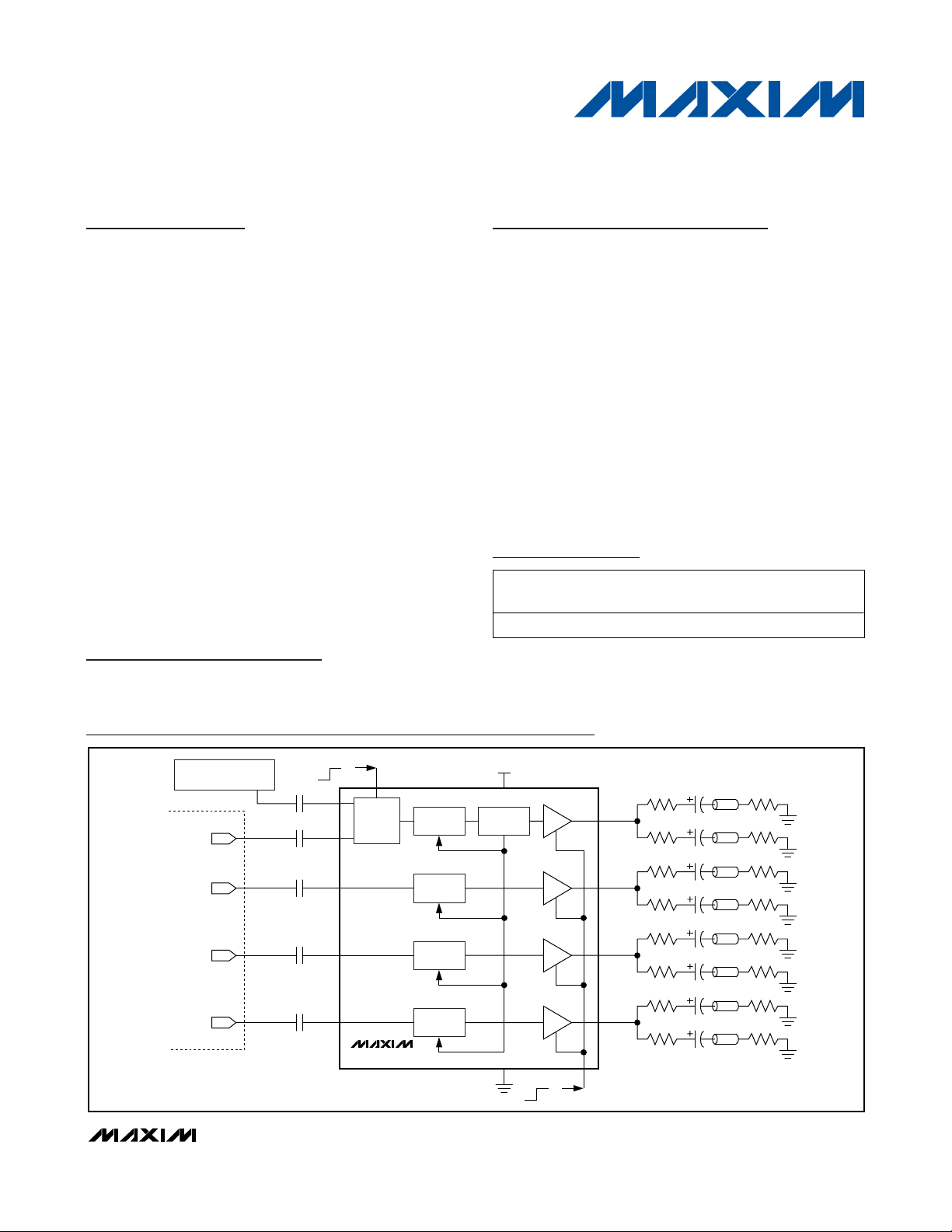
MAX7457
Video Switch for Dual SCART Connectors
________________________________________________________________ Maxim Integrated Products 1
Ordering Information
MAX7457
75Ω
75Ω
*
*
75Ω
75Ω
OUTA
+6dB
75Ω
75Ω
*
*OPTIONAL CAPACITORS
*
75Ω
75Ω
OUTB
+6dB
75Ω
75Ω
*
*
75Ω
75Ω
OUTC
+6dB
75Ω
75Ω
*
*
75Ω
75Ω
OUTD
+6dB
SYNC
DETECTOR
LOWPASS
FILTER
LOWPASS
FILTER
LOWPASS
FILTER
LOWPASS
FILTER
2-TO-1
MUX
GND
DISABLE
SELA
V
CC
0.1µF
INA2
0.1µF
INA1
0.1µF
INB
0.1µF
INC
0.1µF
IND
D/A
D/A
D/A
D/A
AUXILIARY VIDEO SOURCE
(VCR, DVD, ETC.)
ENCODER
CVBS
R
B
G
Typical Operating Circuit
19-3560; Rev 0; 1/05
For pricing, delivery, and ordering information, please contact Maxim/Dallas Direct! at
1-888-629-4642, or visit Maxim’s website at www.maxim-ic.com.
Pin Configuration appears at end of data sheet.
*EP = Exposed pad.
PART TEMP RANGE PIN-PACKAGE
MAX7457ETE -40°C to +85°C 16 TQFN-EP* T1655-2
PKG
CODE
Page 2
MAX7457
Video Switch for Dual SCART Connectors
2 _______________________________________________________________________________________
ABSOLUTE MAXIMUM RATINGS
ELECTRICAL CHARACTERISTICS
(V
CC
= +5V ±5%, CL= 0 to 20pF, RL= 75Ω to GND for DC-coupled load, RL= 75Ω to VCC/2 for AC-coupled load, TA= T
MIN
to
T
MAX
, unless otherwise noted. Typical values are at VCC= 5V, TA= +25°C.)
Stresses beyond those listed under “Absolute Maximum Ratings” may cause permanent damage to the device. These are stress ratings only, and functional
operation of the device at these or any other conditions beyond those indicated in the operational sections of the specifications is not implied. Exposure to
absolute maximum rating conditions for extended periods may affect device reliability.
VCCto GND..............................................................-0.3V to +6V
INA1, INA2, INB, INC, IND to GND ............-0.3V to (V
CC
+ 0.3V)
OUTA, OUTB, OUTC, OUTD to GND.........-0.3V to (V
CC
+ 0.3V)
SELA, DISABLE to GND.............................-0.3V to (V
CC
+ 0.3V)
Maximum Current into Any Pin Except V
CC
and GND .....±50mA
Continuous Power Dissipation (T
A
= +70°C)
16-Pin TQFN (derate 20.8mW/°C
above +70°C)..........................................................1666.7mW
Operating Temperature Range ...........................-40°C to +85°C
Storage Temperature Range .............................-65°C to +150°C
Junction Temperature......................................................+150°C
Lead Temperature (soldering, 10s) .................................+300°C
)
(
)
Passband Flatness
Stopband Attenuation A
Differential Gain dG 5-step modulated staircase 0.15 0.5 %
Differential Phase dθ 5-step modulated staircase 0.15 0.5 Degrees
Signal-to-Noise Ratio SNR
Group Delay Deviation ∆t
Line-Time Distortion H
Field-Time Distortion V
Clamp Settling Time t
Output DC Clamp Level
Low-Frequency Gain Accuracy A
Low-Frequency Gain Matching A
Group Delay Matching
Channel-to-Channel Crosstalk X
Disabled Output Impedance Z
Output Short-Circuit Current I
PARAMETER SYMBOL CONDITIONS MIN TYP MAX UNITS
f = 100kHz to 5MHz,
relative to 100kHz
f ≥ 27MHz 40 43 dB
SB
Peak signal (2V
to 50MHz
Deviation from
g
100kHz to 4.1MHz
DIST
DIST
CLAMP
18µs, 100 IRE bar 0.3 %
130 lines, 18µs, 100 IRE bar 0.5 %
To ±1% 300 Lines
Channel INA_ 0.6 0.9 1.1
Channel INB, INC, IND 1.1 1.5 1.8
f = 100kHz, relative to gain of +6dB -3 +3 %
V
V(MATCH
t
g
MATCH
TALK
DISABLE
SC
Low-frequency channel-to-channel
matching, f = 100kHz
Low-frequency channel-to-channel
matching, f = 100kHz
f = 100kHz to 3.58MHz -60 dB
At 5MHz 2 kΩ
OUT_ shorted to GND or V
Channel INA_ +0.9 +1.2 +1.5
Channels INB,
INC, IND
) to RMS noise, f = 100Hz
P-P
-0.75 +0.15 +0.75
80 dB
Channel INA_ 17 30
Channels INB,
INC, IND
11 20
4%
2ns
CC
70 mA
dB
ns
V
Page 3
MAX7457
Video Switch for Dual SCART Connectors
_______________________________________________________________________________________ 3
ELECTRICAL CHARACTERISTICS (continued)
(V
CC
= +5V ±5%, CL= 0 to 20pF, RL= 75Ω to GND for DC-coupled load, RL= 75Ω to VCC/2 for AC-coupled load, TA= T
MIN
to
T
MAX
, unless otherwise noted. Typical values are at VCC= 5V, TA= +25°C.)
Typical Operating Characteristics
(VCC= +5V, TA= +25°C, unless otherwise noted.)
AMPLITUDE vs. FREQUENCY
MAX7457 toc01
FREQUENCY (MHz)
AMPLITUDE (dB)
10
-60
-40
-20
0
-80
1100
CHANNEL INA_
PASSBAND AMPLITUDE vs. FREQUENCY
MAX7457 toc02
FREQUENCY (MHz)
AMPLITUDE (dB)
1
-1.5
-1.0
-0.5
0
0.5
1.0
1.5
2.0
-2.0
0.1 10
CHANNEL INA_
CHANNELS INB/INC/IND
PHASE RESPONSE vs. FREQUENCY
MAX7457 toc03
FREQUENCY (MHz)
PHASE (DEGREES)
1
-150
-100
-50
0
50
100
150
200
-200
0.1 10
Input Leakage Current I
Input Dynamic Swing
Mux Crosstalk f = 100kHz to 4.1MHz -60 dB
SUPPLY
Supply Voltage Range V
Supply Current I
Power-Supply Rejection Ratio PSRR V
LOGIC INTERFACE
Logic Input High Voltage V
Logic Input Low Voltage V
Logic Input Current VIL = 0 (sink), VIH = V
PARAMETER SYMBOL CONDITIONS MIN TYP MAX UNITS
IN
10 µA
Channel INA_ 1.2
Channels INB, INC, IND 0.9
CC
CC
No load 100 140 mA
= 100mV
IN
IH
IL
, f = 0 to 3.5MHz 40 dB
P-P
(source) ±10 µA
CC
4.75 5.25 V
2.0 V
0.8 V
V
P-P
Page 4

MAX7457
Video Switch for Dual SCART Connectors
4 _______________________________________________________________________________________
Typical Operating Characteristics (continued)
(VCC= +5V, TA= +25°C, unless otherwise noted.)
GROUP DELAY vs. FREQUENCY
100
90
80
70
GROUP DELAY (ns)
60
50
40
0.1 10
FREQUENCY (MHz)
SUPPLY CURRENT vs. TEMPERATURE
120
INPUTS BIASED TO +2V
NO LOAD
110
100
SUPPLY CURRENT (mA)
90
80
-40 85
TEMPERATURE (°C)
2T RESPONSE
(1 IRE = 7.14mV)
MAX7457 toc04
1
IN_
300mV/div
OUT_
300mV/div
200ns/div
MAX7457 toc05
300mV/div
OUT_
300mV/div
DIFFERENTIAL GAIN
0.3
0.2
MAX7457 toc07
0.1
0
-0.1
-0.2
-0.3
DIFFERENTIAL GAIN (%)
MAX7457 toc08
250mV/div
6543217
MODULATED 12.5T RESPONSE
(1 IRE = 7.14mV)
IN_
MULTIBURST RESPONSE
IN_
MAX7457 toc06
400µs/div
MAX7457 toc09
DIFFERENTIAL PHASE
0.3
0.2
0.1
0
-0.1
(DEGREES)
-0.2
-0.3
603510-15
DIFFERENTIAL PHASE
17
65432
OUT_
250mV/div
10µs/div
Page 5

MAX7457
Video Switch for Dual SCART Connectors
_______________________________________________________________________________________ 5
Pin Description
Detailed Description
The MAX7457 4-channel video switch filters and
buffers video encoder DAC outputs in applications
such as STBs, HDRs, DVD players, and digital VCRs.
The MAX7457 offers an auxiliary CVBS loop-through
feature required in dual SCART applications. Audio and
video switching in SCART STBs utilize a costly integrated A/V switch offering high-end features such as volume control and high audio-drive capability. A more
cost-effective solution uses the MAX7457 for the video
switching along with low-cost standard passive analog
switches for the audio switching.
The MAX7457 reconstructs and cleans up analog video
signals from the video encoder’s DAC output. Each
channel consists of a lowpass filter and an output video
buffer that drives two standard 150Ω video loads. The
MAX7457 operates from a single +5V supply and has a
nominal cutoff frequency of 5MHz, optimized for NTSC,
PAL, and SDTV.
Filter
Filter Response
The reconstruction filter consists of two 2nd-order
Sallen-Key stages. The Butterworth-type response features a maximally flat passband for NTSC and PAL
bandwidths. The stopband offers at least 43dB (typ) of
attenuation at the video encoder’s DAC sampling frequency of 27MHz (see the Typical Operating
Characteristics).
High-Frequency Boost
INA1/INA2 have +1.2dB of high-frequency boost that
increases image sharpness by compensating for signal degradation and rolloff in the video encoder.
Channels INB/INC/IND (RGB) do not boost high-frequency signals and have a flat response over the
video bandwidth.
PIN NAME FUNCTION
1 INB
2 INC
3 IND
4 DISABLE
5 SELA Select A Input. A logic low on SELA selects INA1 and a logic high on SELA selects INA2.
6, 8, 14 N.C. No Connection. Not internally connected.
7 GND Ground
9VCC+5V Supply Input
10 OUTD Channel D Video Output. OUTD can be either AC- or DC-coupled.
11 OUTC Channel C Video Output. OUTC can be either AC- or DC-coupled.
12 OUTB Channel B Video Output. OUTB can be either AC- or DC-coupled.
13 OUTA Channel A Video Output. OUTA can be either AC- or DC-coupled.
15 INA2
16 INA1 Channel INA1 Video Input. Connect CVBS to INA1. AC-couple INA1 with a series 0.1µF capacitor.
— EP Exposed Pad. Connect to GND for improved thermal heat sinking.
Channel INB Video Input. Use channel INB for the red (R) signal. AC-couple INB with a series
0.1µF capacitor.
Channel INC Video Input. Use channel INC for the green (G) signal. AC-couple INC with a series
0.1µF capacitor.
Channel IND Video Input. Use channel IND for the blue (B) signal. AC-couple IND with a series
0.1µF capacitor.
Disable Logic Input. A logic low on DISABLE enables the output buffers. A logic high on DISABLE
disables all buffer outputs and puts them in a high-impedance state.
Channel INA2 Video Input. Connect auxiliary CVBS to INA2. AC-couple INA2 with a series
0.1µF capacitor.
Page 6

MAX7457
Output Buffers
Each output buffer has a fixed gain of +6dB and can
drive two 150Ω video loads with a 2V
P-P
signal. The
MAX7457 can drive an AC-coupled load or drive a DCcoupled load, eliminating the large coupling capacitors. The output buffers drive DC loads with an output
blanking level of less than 1V.
Output Clamp Level
The video signal processed by channel INA_ (CVBS
video signal) must include a sync pulse. This sync
pulse provides the required timing to all four channels.
When channel INA_ detects a sync pulse, the DC
restore loop is activated. The function of the loop is to
set the DC level of the video signal to a specified voltage. See Table 1 for clamp levels.
Input Multiplexer
The MAX7457 has a 2-to-1 input multiplexer at channel
INA_. The input to the CVBS channel comes from
either a DAC output or from a CVBS source and is
selected by SELA. Pull SELA low to select INA1 or high
to select INA2.
Applications Information
Input Considerations
Use 0.1µF ceramic capacitors to AC-couple the inputs.
The input capacitors store a DC level so the outputs are
clamped to an appropriate DC voltage level.
Output Considerations
The outputs are typically connected to a 75Ω series
back-match resistor followed by the video cable.
Because of the inherent divide-by-two of this configuration, the voltage on the video cable is always less than
1V, complying with industry-standard video requirements such as the European SCART standard (which
allows up to 2V of DC on the video cable). The video
buffer can also drive an AC-coupled video load. An
output capacitor as low as 220µF provides good
video performance.
Power-Supply Bypassing and Layout
The MAX7457 operates from a single +5V supply.
Bypass VCCto GND with a 0.1µF capacitor. Place all
external components as close to the device as possible.
Exposed Pad
The TQFN package has an exposed pad on the bottom
of the package. This pad is electrically connected to
GND and should be connected to the ground plane for
improved thermal conductivity. Do not route signals
under this package.
Video Switch for Dual SCART Connectors
6 _______________________________________________________________________________________
Chip Information
TRANSISTOR COUNT: 4579
PROCESS: BiCMOS
Pin Configuration
Table 1. Output Clamp Level
CHANNEL CLAMP LEVEL (V)
A 0.9
B 1.5
C 1.5
D 1.5
TOP VIEW
INB
INC
IND
DISABLE
INA1
INA2
16
15 14 13
1
2
3
4
MAX7457
5678
N.C.
SELA
TQFN
N.C.
GND
OUTA
N.C.
OUTB
12
OUTC
11
OUTD
10
V
9
CC
Page 7

MAX7457
Video Switch for Dual SCART Connectors
_______________________________________________________________________________________ 7
Package Information
(The package drawing(s) in this data sheet may not reflect the most current specifications. For the latest package outline information
go to www.maxim-ic.com/packages
.)
MARKING
PIN # 1
I.D.
C
-DRAWING NOT TO SCALE-
D
AAAAA
D2
C
D/2
E/2
E
e
L1
0.10 C
A
0.08 C
A3
A1
(NE-1) X e
DETAIL A
L
L
L
k
e
(ND-1) X e
L
e e
PACKAGE OUTLINE,
16, 20, 28, 32, 40L THIN QFN, 5x5x0.8mm
b
D2/2
0.10 M C A B
I
L
1
2
QFN THIN.EPS
L
E2/2
C
E2
L
DETAIL B
PIN # 1 I.D.
0.35x45°
CC
L
e/2
21-0140
PKG.
SYMBOL
A
A1
A3
b
D
E
e
k
L
L1
N
ND
NE
JEDEC
NOTES:
1. DIMENSIONING & TOLERANCING CONFORM TO ASME Y14.5M-1994.
2. ALL DIMENSIONS ARE IN MILLIMETERS. ANGLES ARE IN DEGREES.
3. N IS THE TOTAL NUMBER OF TERMINALS.
4. THE TERMINAL #1 IDENTIFIER AND TERMINAL NUMBERING CONVENTION SHALL
CONFORM TO JESD 95-1 SPP-012. DETAILS OF TERMINAL #1 IDENTIFIER ARE
OPTIONAL, BUT MUST BE LOCATED WITHIN THE ZONE INDICATED. THE TERMINAL #1
IDENTIFIER MAY BE EITHER A MOLD OR MARKED FEATURE.
5. DIMENSION b APPLIES TO METALLIZED TERMINAL AND IS MEASURED BETWEEN
0.25 mm AND 0.30 mm FROM TERMINAL TIP.
6. ND AND NE REFER TO THE NUMBER OF TERMINALS ON EACH D AND E SIDE RESPECTIVELY.
7. DEPOPULATION IS POSSIBLE IN A SYMMETRICAL FASHION.
8. COPLANARITY APPLIES TO THE EXPOSED HEAT SINK SLUG AS WELL AS THE TERMINALS.
9. DRAWING CONFORMS TO JEDEC MO220, EXCEPT EXPOSED PAD DIMENSION FOR
T2855-3 AND T2855-6.
10. WARPAGE SHALL NOT EXCEED 0.10 mm.
11. MARKING IS FOR PACKAGE ORIENTATION REFERENCE ONLY.
12. NUMBER OF LEADS SHOWN ARE FOR REFERENCE ONLY.
13. LEAD CENTERLINES TO BE AT TRUE POSITION AS DEFINED BY BASIC DIMENSION "e", ±0.05.
-DRAWING NOT TO SCALE-
COMMON DIMENSIONS
16L 5x5
MIN. MAX.NOM.
0.70 0.800.75
0.05
0.02
0.20 REF.
0.25
0.350.30
4.90
5.10
5.00
4.90
5.105.00
0.80 BSC.
0.250--
0.30 0.500.40
--- --16
4
4
WHHB
MIN.
0.70
0
0.20 REF.
0.25
4.90
4.90
0.25
0.45
20L 5x5
NOM.
0.75
0.02
0.30
5.00
5.00
0.65 BSC.
0.55
20
5
5
WHHC
MAX.
0.80
0.05
0.35
5.10
5.10
0.65
28L 5x5
MIN.
0.70
0
0.20 REF.
0.20
4.90
4.90
0.50 BSC.
--
0.25
0.45
---
WHHD-1
NOM.
0.75
0.02
0.25
5.00
5.00
0.55
28
7
7
MAX.
0.80
0.05
0.30
5.10
5.10
0.65
--
32L 5x5
NOM.
MIN.
0.70
0.75
0
0.02
0.20 REF.
0.20 0.25 0.30
5.00
4.90
5.00
4.90
0.50 BSC.
0.25
0.40
0.30
--32
8
8
WHHD-2
MAX.
MIN.
0.70
0.80
0.05
0.15
5.10
4.90
5.10
4.90 5.00
--
0.25 0.35 0.45
0.50
0.30
40L 5x5
NOM.
0.75 0.80
0.20 REF.
5.00 5.10
0.40 BSC.
0.40 0.50
40
10
10
-----
MAX.
0.050 0.02
0.250.20
5.10
0.600.40 0.50
EXPOSED PAD VARIATIONS
PKG.
CODES
T1655-2
D2
NOM.MIN.
T2055-4
T2855-3 3.15 3.25 3.35 3.15 3.25 3.35
T2855-4 2.60 2.70 2.80 2.60 2.70 2.80
T2855-5 2.60 2.70 2.80 2.60 2.70 2.80
3.15 3.25 3.35 3.15 3.25 3.35
T2855-6
T2855-7 2.60 2.70
3.15
T2855N-1
3.25 3.15 3.25 3.35
3.00 3.10T3255-3 3 3.203.00 3.10
T3255-5 YES3.003.103.00
3.30T4055-1 3.20 3.40 3.20 3.30 3.40
PACKAGE OUTLINE,
16, 20, 28, 32, 40L THIN QFN, 5x5x0.8mm
E2
NOM. MAX.
MIN.
MAX.
3.203.00T1655-3 3.10 3.00 3.10 3.20 NO
3.103.00 3.203.103.00 3.20
3.353.15T2055-5 3.25 3.15 3.25 3.35
2.80
2.60 2.70 2.80
3.353.15T2855-8 3.25 3.15 3.25 3.35
3.35
3.20
3.203.00 3.10T3255-4 3 3.203.00 3.10
3.20
3.203.10T3255N-1 3.00
3.203.10
3.203.103.00
SEE COMMON DIMENSIONS TABLE
**
21-0140
exceptions
±0.15
0.40
0.40
DOWN
L
BONDS
ALLOWED
YES3.203.103.003.103.00 3.20
**
**
NO3.203.103.003.10T1655N-1 3.00 3.20
**
YES3.103.00 3.203.103.00 3.20T2055-3
**
NO
**
YES
YES
**
YES
**
NO
**
NO
**
YES
**
YES
NO
**
YES
**
NO
**
**
NO
**
YES
**
2
I
2
Page 8

MAX7457
Video Switch for Dual SCART Connectors
Maxim cannot assume responsibility for use of any circuitry other than circuitry entirely embodied in a Maxim product. No circuit patent licenses are
implied. Maxim reserves the right to change the circuitry and specifications without notice at any time.
8 _____________________Maxim Integrated Products, 120 San Gabriel Drive, Sunnyvale, CA 94086 408-737-7600
© 2005 Maxim Integrated Products Printed USA is a registered trademark of Maxim Integrated Products, Inc.
Package Information (continued)
(The package drawing(s) in this data sheet may not reflect the most current specifications. For the latest package outline information
go to www.maxim-ic.com/packages
.)
D
D/2
MARKING
PIN # 1
I.D.
-DRAWING NOT TO SCALE-
PKG.
SYMBOL
A
A1
A3
b
D
E
e
k
L
L1
N
ND
NE
JEDEC
NOTES:
1. DIMENSIONING & TOLERANCING CONFORM TO ASME Y14.5M-1994.
2. ALL DIMENSIONS ARE IN MILLIMETERS. ANGLES ARE IN DEGREES.
3. N IS THE TOTAL NUMBER OF TERMINALS.
4. THE TERMINAL #1 IDENTIFIER AND TERMINAL NUMBERING CONVENTION SHALL
CONFORM TO JESD 95-1 SPP-012. DETAILS OF TERMINAL #1 IDENTIFIER ARE
OPTIONAL, BUT MUST BE LOCATED WITHIN THE ZONE INDICATED. THE TERMINAL #1
IDENTIFIER MAY BE EITHER A MOLD OR MARKED FEATURE.
5. DIMENSION b APPLIES TO METALLIZED TERMINAL AND IS MEASURED BETWEEN
0.25 mm AND 0.30 mm FROM TERMINAL TIP.
6. ND AND NE REFER TO THE NUMBER OF TERMINALS ON EACH D AND E SIDE RESPECTIVELY.
7. DEPOPULATION IS POSSIBLE IN A SYMMETRICAL FASHION.
8. COPLANARITY APPLIES TO THE EXPOSED HEAT SINK SLUG AS WELL AS THE TERMINALS.
9. DRAWING CONFORMS TO JEDEC MO220, EXCEPT EXPOSED PAD DIMENSION FOR
T2855-3 AND T2855-6.
10. WARPAGE SHALL NOT EXCEED 0.10 mm.
11. MARKING IS FOR PACKAGE ORIENTATION REFERENCE ONLY.
12. NUMBER OF LEADS SHOWN ARE FOR REFERENCE ONLY.
13. LEAD CENTERLINES TO BE AT TRUE POSITION AS DEFINED BY BASIC DIMENSION "e", ±0.05.
-DRAWING NOT TO SCALE-
AAAAA
C
COMMON DIMENSIONS
16L 5x5
MIN. MAX.NOM.
0.70 0.800.75
0.05
0.02
0.20 REF.
0.350.30
0.25
5.10
5.00
4.90
5.105.00
4.90
0.80 BSC.
0.250--
0.30 0.500.40
--16
4
4
WHHB
MIN.
0.70
0
0.20 REF.
0.25
4.90
4.90
0.25
0.45
---
20L 5x5
NOM.
0.75
0.02
0.30
5.00
5.00
0.65 BSC.
0.55
20
5
5
WHHC
MAX.
0.80
0.05
0.35
5.10
5.10
0.65
E/2
E
e
L
L1
0.10 C
A
0.08 C
A3
A1
28L 5x5
32L 5x5
NOM.
0.75
0.02
5.00
5.00
0.50 BSC.
0.40
32
8
8
WHHD-2
MAX.
MIN.
0.70
0.80
0.05
0.15
5.10
4.90
5.10
4.90 5.00
--
0.25 0.35 0.45
0.50
0.30
40L 5x5
NOM.
0.75 0.80
0.20 REF.
5.00 5.10
0.40 BSC.
0.40 0.50
40
10
10
-----
MAX.
0.050 0.02
0.250.20
5.10
0.600.40 0.50
NOM.
MIN.
MAX.
MIN.
0.70
0.80
0.70
0.75
0
0.05
0
0.02
0.20 REF.
0.20 REF.
0.30
0.20
0.20 0.25 0.30
0.25
5.10
4.90
5.00
4.90
5.10
4.90
5.00
4.90
0.50 BSC.
--
0.25
0.45
---
0.55
28
7
7
WHHD-1
--
0.25
0.65
0.30
---
D2
C
L
D2/2
k
(NE-1) X e
DETAIL A
L
EXPOSED PAD VARIATIONS
PKG.
CODES
T1655-2
T2055-4
T2855-3 3.15 3.25 3.35 3.15 3.25 3.35
T2855-4 2.60 2.70 2.80 2.60 2.70 2.80
T2855-5 2.60 2.70 2.80 2.60 2.70 2.80
3.15 3.25 3.35 3.15 3.25 3.35
T2855-6
T2855-7 2.60 2.70
3.15
T2855N-1
3.00 3.10T3255-3 3 3.203.00 3.10
T3255-5 YES3.003.103.00
e/2
e
(ND-1) X e
L
e e
PACKAGE OUTLINE,
16, 20, 28, 32, 40L THIN QFN, 5x5x0.8mm
D2
MAX.
NOM.MIN.
3.203.00T1655-3 3.10 3.00 3.10 3.20 NO
3.353.15T2055-5 3.25 3.15 3.25 3.35
2.80
3.353.15T2855-8 3.25 3.15 3.25 3.35
3.25 3.15 3.25 3.35
3.35
3.20
3.203.00 3.10T3255-4 3 3.203.00 3.10
3.20
3.203.10T3255N-1 3.00
3.30T4055-1 3.20 3.40 3.20 3.30 3.40
PACKAGE OUTLINE,
16, 20, 28, 32, 40L THIN QFN, 5x5x0.8mm
b
0.10 M C A B
L
E2/2
C
E2
L
PIN # 1 I.D.
0.35x45°
DETAIL B
CC
21-0140
E2
exceptions
±0.15
NOM. MAX.
MIN.
3.103.00 3.203.103.00 3.20
0.40
2.60 2.70 2.80
**
0.40
3.203.10
3.203.103.00
SEE COMMON DIMENSIONS TABLE
21-0140
QFN THIN.EPS
L
L
1
I
2
DOWN
L
BONDS
ALLOWED
YES3.203.103.003.103.00 3.20
**
**
NO3.203.103.003.10T1655N-1 3.00 3.20
**
YES3.103.00 3.203.103.00 3.20T2055-3
**
NO
**
YES
YES
**
YES
**
NO
**
NO
**
YES
**
YES
NO
**
YES
**
NO
**
**
NO
**
YES
**
2
I
2
 Loading...