

Page 1
General Description
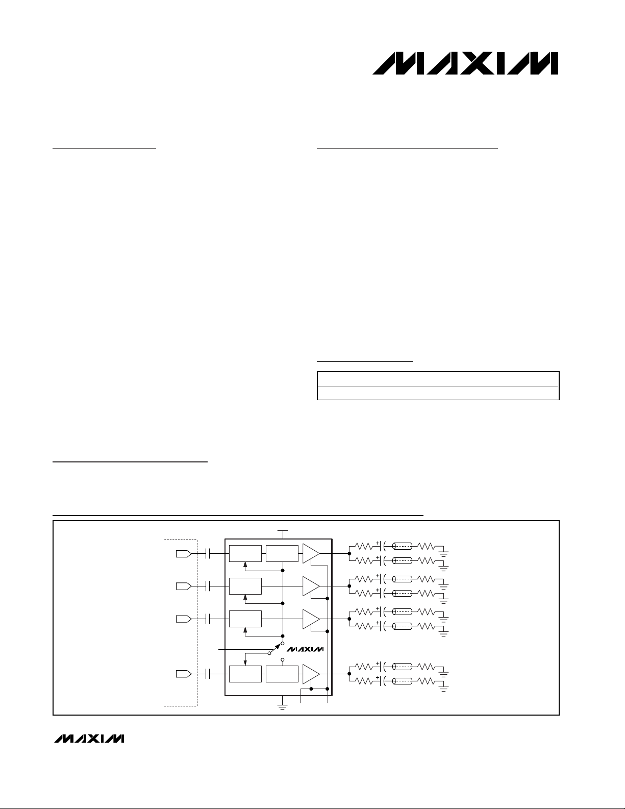
The MAX7445 4-channel, buffered video reconstruction
filter is ideal for anti-aliasing and DAC-smoothing video
applications or wherever analog video is reconstructed
from a digital data stream (such as cable/satellite/terrestrial set-top boxes, DVD players, hard-disk recorders
(HDRs), and personal video recorders (PVRs)). This
device operates from a single +5V supply and has a
flat passband out to 5MHz with a stopband attenuation
of 43dB at 27MHz. This makes it ideal for use with
NTSC, PAL, and standard-definition digital TV (SDTV)
video systems. Each output is capable of driving two
standard 150Ω video loads.
The MAX7445 has three modes of operation. Mode 1
processes CVBS and RGB video signals. Mode 2
processes CVBS, Y, and C signals, as well as a second
asynchronous CVBS video signal. Mode 3 processes
RGB and CVBS (asynchronous) video signals. An external pin adjusts the gain of the video buffer to either +6dB,
+9.5dB, or +12dB to accommodate video-encoder DAC
output signals of <1V. High-frequency boost circuitry provides picture sharpness with +1.2dB of gain boost without degradation in the stopband. The output video drivers
can be disabled with an external pin.
The MAX7445 is available in a 14-pin TSSOP package
with an exposed pad, and is specified over the -40°C to
+85°C extended temperature range.
Applications
Set-Top Boxes/HDRs DVD Players
Game Consoles Digital VCRs
Desktop Video Editors
Features
♦ 4-Channel Filter and Buffer for CVBS, RGB, or Y/C
Video Signals
♦ Filter Response Ideal for NTSC, PAL, and
Interlaced SDTV Video Signals
♦ 43dB (typ) Stopband Attenuation at 27MHz
♦ ±0.75dB (max) Passband Ripple Out to 5MHz
♦ Blanking Level Voltage on Cable <1V
♦ Each Channel Drives Two 150Ω Video Loads
♦ +5V Single-Supply Voltage
♦ Selectable Gain: +6dB, +9.5dB, and +12dB
♦ Small 14-Pin TSSOP Package
MAX7445
4-Channel Video Reconstruction Filter
________________________________________________________________ Maxim Integrated Products 1
Functional Diagram
Ordering Information
19-2948; Rev 0; 8/03
For pricing, delivery, and ordering information, please contact Maxim/Dallas Direct! at
1-888-629-4642, or visit Maxim’s website at www.maxim-ic.com.
*EP = Exposed pad.
Pin Configuration appears at end of data sheet.
PART TEMP RANGE PIN-PACKAGE
MAX7445EUD -40°C to +85°C 14 TSSOP-EP*
ENCODER
0.1µF
INA
D/A
0.1µF
D/A
0.1µF
D/A
SELECT
0.1µF
D/A
LOWPASS
FILTER
INB
LOWPASS
FILTER
INC
LOWPASS
FILTER
IND
LOWPASS
FILTER
V
SYNC
DETECTOR
SYNC
DETECTOR
GND
CC
75Ω
75Ω
75Ω
75Ω
75Ω
75Ω
75Ω
75Ω
MAX7445
DISABLE
OUTA
OUTB
OUTC
OUTD
GAIN
75Ω
*
75Ω
*
75Ω
*
75Ω
*
75Ω
*
75Ω
*
75Ω
*
75Ω
*
*OPTIONAL CAPACITORS
Page 2
MAX7445
4-Channel Video Reconstruction Filter
2 _______________________________________________________________________________________
ABSOLUTE MAXIMUM RATINGS
ELECTRICAL CHARACTERISTICS
(VCC= +5V ±5%, CL= 0 to 20pF, RL= 75Ω to GND for DC-coupled load, RL= 75Ω to VCC/ 2 for AC-coupled load, C
IN_
= 0.1µF,
GAIN = GND (+6dB) or V
CC
(+9.5dB), TA= T
MIN
to T
MAX
, unless otherwise noted. Typical values are at VCC= +5V, TA= +25°C.)
Stresses beyond those listed under “Absolute Maximum Ratings” may cause permanent damage to the device. These are stress ratings only, and functional
operation of the device at these or any other conditions beyond those indicated in the operational sections of the specifications is not implied. Exposure to
absolute maximum rating conditions for extended periods may affect device reliability.
VCCto GND ...........................................................................+6V
All Other Pins to GND.................................-0.3V to (V
CC
+ 0.3V)
Maximum Current into Any Pin Except V
CC
and GND .....±50mA
Continuous Power Dissipation (T
A
= +70°C)
TSSOP-EP (derate 20.8mW/°C above +70°C)...........1667mW
Operating Temperature Range ...........................-40°C to +85°C
Storage Temperature Range .............................-65°C to +150°C
Junction Temperature......................................................+150°C
Lead Temperature (soldering, 10s) .................................+300°C
Passband Response
Stopband Attenuation A
Differential Gain dG
Differential Phase dθ
Signal-to-Noise Ratio SNR
PARAMETER SYMBOL CONDITIONS MIN TYP MAX UNITS
f = 100kHz to 5MHz,
relative to 100kHz
f ≥ 27MHz 39 43 dB
SB
5-step modulated
staircase
5-step modulated
staircase
Peak signal (2V
RMS noise,
f = 100Hz to 50MHz
P-P
Channel without
boost (see Table 2)
Channel with boost
(see Table 2)
Gain = +6dB,
+9.5dB
Gain = +12dB 0.25 0.90
Gain = +6dB,
+9.5dB
Gain = +12dB 0.15 0.60
) to
Gain = +6dB,
+9.5dB, +12dB
-0.75 +0.15 +0.75
+0.9 +1.2 +1.5
0.15 0.50
0.15 0.50
69 75 dB
dB
%
Degrees
Channel without
Group Delay Deviation
Line-Time Distortion H
Field-Time Distortion V
Clamp Settling Time t
Output DC Clamp Level
Low-Frequency Gain Accuracy A
Low-Frequency Gain Matching A
∆t
DIST
DIST
CLAMP
V ( M ATC H )
Deviation from 100kHz
g
to 4.1MHz
18µs, 100 IRE bar 0.3 %
130 lines, 18µs, 100 IRE bar 0.5 %
To ±1% 100 Lines
SELECT = GND
SELECT = V
SELECT = floating
f = 100kHz, relative to a gain of +6dB -3 +3 %
V
Low-frequency channel-to-channel matching,
f = 100kHz
CC
boost (see Table 2)
Channel with boost
(see Table 2)
Channel A 0.6 0.9 1.1
Channels B, C, D 1.1 1.5 1.8
Channels A, B, D 0.6 0.9 1.1
Channel C 1.25 1.6 1.95
Channels A, D 0.6 0.9 1.1
Channels B, C 1.1 1.5 1.8
11 20
17 30
ns
V
4%
Page 3
MAX7445
4-Channel Video Reconstruction Filter
_______________________________________________________________________________________ 3
ELECTRICAL CHARACTERISTICS (continued)
(VCC= +5V ±5%, CL= 0 to 20pF, RL= 75Ω to GND for DC-coupled load, RL= 75Ω to VCC/ 2 for AC-coupled load, C
IN_
= 0.1µF,
GAIN = GND (+6dB) or V
CC
(+9.5dB), TA= T
MIN
to T
MAX
, unless otherwise noted. Typical values are at VCC= +5V, TA= +25°C.)
Group Delay Matching
Channel-to-Channel Crosstalk X
Output Short-Circuit Current I
Input Leakage Current I
Input Dynamic Swing for Gain
of +6dB
SUPPLY
Supply Voltage Range V
Supply Current I
Power-Supply Rejection Ratio PSRR V
DISABLE
Output Impedance During
Disable
D i sab l e Log i c- Inp ut H i g h V ol tag eV
D i sab l e Log i c- Inp ut Low V ol tag eV
Disable Logic Input Current I
PARAMETER SYMBOL CONDITIONS MIN TYP MAX UNITS
t
g(MATCH)
Z
DISABLEVIL
TALK
SC
IN
CC
CC
DISABLE
IH
IL
Low-frequency channel-to-channel matching,
f = 100kHz
f = 100kHz to 3.58MHz 60 dB
OUT_ shorted to GND or V
SELECT = GND
SELECT = V
SELECT = floating
No load 100 140 mA
IN
At 5MHz 2 kΩ
2ns
CC
Channel A 1.2
Channels B, C, D 0.9
CC
= 100mV
= 0V (sink), VIH = VCC (source) ±10 µA
, f = 0 to 3.5MHz 40 dB
P-P
Channels A, B, D 1.2
Channel C 0.9
Channels A, D 1.2
Channels B, C 0.9
4.75 5.25 V
2.0 V
70 mA
10 µA
0.8 V
V
P-P
Page 4

MAX7445
4-Channel Video Reconstruction Filter
4 _______________________________________________________________________________________
Typical Operating Characteristics
(VCC= +5V, V
GAIN
= 0V, TA = +25°C, unless otherwise noted.)
AMPLITUDE vs. FREQUENCY
MAX7445 toc01
FREQUENCY (MHz)
AMPLITUDE (dB)
10
-80
-60
-40
-20
0
1 100
NORMALIZED TO 0dB
PASSBAND AMPLITUDE vs. FREQUENCY
FREQUENCY (MHz)
AMPLITUDE (dB)
1
-1.5
-1.0
-0.5
0
0.5
1.0
1.5
2.0
-2.0
0.1 10
MAX7445 toc02
NORMALIZED TO 0dB
FLAT PASSBAND RESPONSE
HIGH-FREQUENCY BOOST
PHASE RESPONSE vs. FREQUENCY
MAX7445 toc03
FREQUENCY (MHz)
PHASE (DEGREES)
1
-150
-100
-50
0
50
100
150
200
-200
0.1 10
GROUP DELAY vs. FREQUENCY
MAX7445 toc04
FREQUENCY (MHz)
GROUP DELAY (ns)
1
60
70
80
90
100
50
0.1 10
2T RESPONSE (1 IRE = 7.14mV)
MAX7445 toc05
200ns/div
250mV/
div
IN_
OUT_
250mV/
div
MODULATED 12.5T RESPONSE
(1 IRE = 7.14mV)
MAX7445 toc06
400ns/div
250mV/
div
IN_
OUT_
250mV/
div
SUPPLY CURRENT vs. TEMPERATURE
MAX7445 toc07
TEMPERATURE (°C)
SUPPLY CURRENT (mA)
603510-15
90
100
110
120
80
-40 85
INPUTS BIASED TO +2V
NO LOAD
DIFFERENTIAL GAIN
MAX7445 toc08
DIFFERENTIAL PHASE (DEGREES)
2nd1st 3rd 4th
5th
6th
2nd1st 3rd 4th
5th
6th
0.2
0.3
0.1
0
-0.1
-0.2
-0.3
DIFFERENTIAL GAIN (%)
0.2
0.3
0.1
0
-0.1
-0.2
-0.3
DIFFERENTIAL PHASE
MULTIBURST RESPONSE
MAX7445 toc09
10µs/div
250mV/
div
IN_
OUT_
250mV/
div
Page 5

MAX7445
4-Channel Video Reconstruction Filter
_______________________________________________________________________________________ 5
Detailed Description
The MAX7445 filters and buffers video-encoder DAC
outputs in applications such as set-top boxes, harddisk recorders, DVD players, and digital VCRs. The
MAX7445 reconstructs and cleans up analog video signals from the output of DAC video encoders. Each
channel consists of a lowpass filter and an output video
buffer that can drive two standard 150Ω video loads.
This device operates from a single +5V supply and has
a nominal cutoff frequency of 5MHz optimized for
NTSC, PAL, and SDTV.
The MAX7445 has three modes of operation allowing
different video signals to be processed. The modes are
shown in Table 1. Mode 1 requires that channel A is a
video signal that includes a sync pulse. A sync separator uses this signal to extract the timing required to
clamp all four channels.
Modes 2 and 3 require that channel A and channel D
have a sync pulse to provide the required timing information. Channel A provides the required timing for channels
A, B, and C while channel D provides its own sync separator to extract the sync signal from an asynchronous
video signal.
Filter
Filter Response
The reconstruction filter consists of two 2nd-order SallenKey stages. The Butterworth-type response features a
maximally flat passband for NTSC and PAL bandwidths.
The stopband offers at least 43dB (typ) of attenuation at
a video-encoder DAC sampling frequency of 27MHz
(see the Typical Operating Characteristics).
Pin Description
Table 1. Operating Modes
PIN NAME FUNCTION
1 INA Channel A Video Input. AC-couple INA with a series 0.1µF capacitor.
2 INB Channel B Video Input. AC-couple INB with a series 0.1µF capacitor.
3 INC Channel C Video Input. AC-couple INC with a series 0.1µF capacitor.
4 IND Channel D Video Input. AC-couple IND with a series 0.1µF capacitor.
5 DISABLE
6, 8 GND Ground
7 GAIN
9 SELECT
10 V
11 OUTD Channel D Video Output. This output can be either AC- or DC-coupled.
12 OUTC Channel C Video Output. This output can be either AC- or DC-coupled.
13 OUTB Channel B Video Output. This output can be either AC- or DC-coupled.
14 OUTA Channel A Video Output. This output can be either AC- or DC-coupled.
Disable Logic Input. A logic-low on DISABLE enables the output buffers. A logic-high on DISABLE disables
all output buffers and puts them in a high-impedance state.
Gain-Control Input. Connect GAIN to GND for a gain of +6dB (+2V/V), to V
or leave unconnected for a gain of +12dB (+4V/V).
Mode Select Input. Connect to GND for CVBS/RGB processing, to V
processing, or leave floating for RGB/CVBS
+5V Supply Input
CC
(G with sync) processing.
ASYNC
MODE SELECT CHANNEL SIGNAL
MODE 1
CVBS/RGB
MODE 2
CVBS/Y/C/
CVBS
ASYNC
MODE 3
RGB/CVBS
(G with sync)
ASYNC
for a gain of +9.5dB (+3V/V),
CC
for CVBS/Y/C/CVBS
CC
GND
V
CC
FLOATING
ASYNC
A CVBS
BR
CG
DB
A CVBS
BY
CC
D CVBS
A G (with sync)
BR
CB
D CVBS
ASYNC
ASYNC
Page 6

MAX7445
4-Channel Video Reconstruction Filter
6 _______________________________________________________________________________________
High-Frequency Boost
The high-frequency boost available on the CVBS, Y, and
C video channels increases image sharpness by compensating for signal degradation and roll-off in the video
encoder. Table 2 shows the channels that have the highfrequency boost option for the three operating modes.
The channels without high-frequency boost have a flat
response over the video bandwidth.
Output Buffers
Each output buffer can drive two 150Ω video loads with
a 2V
P-P
signal. The output buffer gain is selectable
between +6dB, +9.5dB, or +12dB by using GAIN (see
Table 3). The MAX7445 can drive an AC load or drive
the video load directly without using a large output
capacitor. The output buffers drive DC loads with an
output blanking level of less than 1V.
12dB Gain Setting
GAIN is biased internally to VCC/ 2 with a resistordivider pair of 100kΩ resistors from VCCto GND such
that the internal impedance at the node is 50kΩ. No
additional connection is necessary since the input
offers a minimum noise-margin immunity of 1V
P-P
.
Output Clamp Level
When sync pulses are detected in either a CVBS or G
video signal, the DC restore loop is activated. The function of the loop is to set the DC level of the video signal
to a specified voltage. See Table 4 for clamp levels.
Applications Information
Input Considerations
Use 0.1µF ceramic capacitors to AC-couple the inputs.
These input capacitors store a DC level so the outputs
are clamped to an appropriate DC voltage level.
Output Considerations
The outputs are typically connected to a 75Ω series
back-match resistor followed by the video cable.
Because of the inherent divide-by-two of this configuration, the voltage on the video cable is always less than
1V, complying with industry-standard video requirements such as the European SCART standard (which
allows up to 2V of DC on the video cable). The video
buffer can also drive an AC-coupled video load. Good
video performance is achieved with an output capacitor
as low as 220µF.
Power-Supply Bypassing and Layout
The MAX7445 operates from a single +5V supply.
Bypass VCCto GND with a 0.1µF capacitor. Place all
external components as close to the device as possible.
Table 2. High-Frequency Boost for Each
Mode
Table 3. Gain Setting Control
Table 4. Output Clamp Level
CHANNEL
A +1.2 +1.2 –
B – +1.2 –
C – +1.2 –
D – +1.2 +1.2
GAIN BUFFER GAIN (dB)
GND +6
V
CC
Floating +12
HIGH-FREQUENCY BOOST (dB)
MODE 1 MODE 2 MODE 3
+9.5
CHANNEL
A 0.8 Channel A 0.8 Channel A 0.8 Channel A
B 1.4 Channel A 0.8 Channel A 1.4 Channel A
C 1.4 Channel A 1.6 Channel A 1.4 Channel A
D 1.4 Channel A 0.8 Channel D 0.8 Channel D
MODE 1: SELECT = GND MODE 2: SELECT = V
CLAMP LEVEL (V) SYNC SOURCE CLAMP LEVEL (V) SYNC SOURCE CLAMP LEVEL (V) SYNC SOURCE
CC
MODE 3: SELECT = FLOATING
Page 7

Exposed Pads
The TSSOP-EP package has an exposed pad on the
bottom of the package. This pad is electrically connected to GND and should be connected to the ground
plane for improved thermal conductivity. Do not route
signals under this package.
Chip Information
TRANSISTOR COUNT: 6300
PROCESS: BiCMOS
MAX7445
4-Channel Video Reconstruction Filter
_______________________________________________________________________________________ 7
Pin Configuration
TOP VIEW
INA
INB
INC
DISABLE
GND
1
2
3
4
5
6
7
14
OUTA
13
OUTB
12
OUTC
11
MAX7445
TSSOP
OUTDIND
V
10
CC
9
SELECT
GNDGAIN
8
Page 8

MAX7445
4-Channel Video Reconstruction Filter
Maxim cannot assume responsibility for use of any circuitry other than circuitry entirely embodied in a Maxim product. No circuit patent licenses are
implied. Maxim reserves the right to change the circuitry and specifications without notice at any time.
8 _____________________Maxim Integrated Products, 120 San Gabriel Drive, Sunnyvale, CA 94086 408-737-7600
© 2003 Maxim Integrated Products Printed USA is a registered trademark of Maxim Integrated Products.
Package Information
(The package drawing(s) in this data sheet may not reflect the most current specifications. For the latest package outline information,
go to www.maxim-ic.com/packages
.)
TSSOP 4.4mm BODY.EPS
 Loading...