

Page 1
General Description
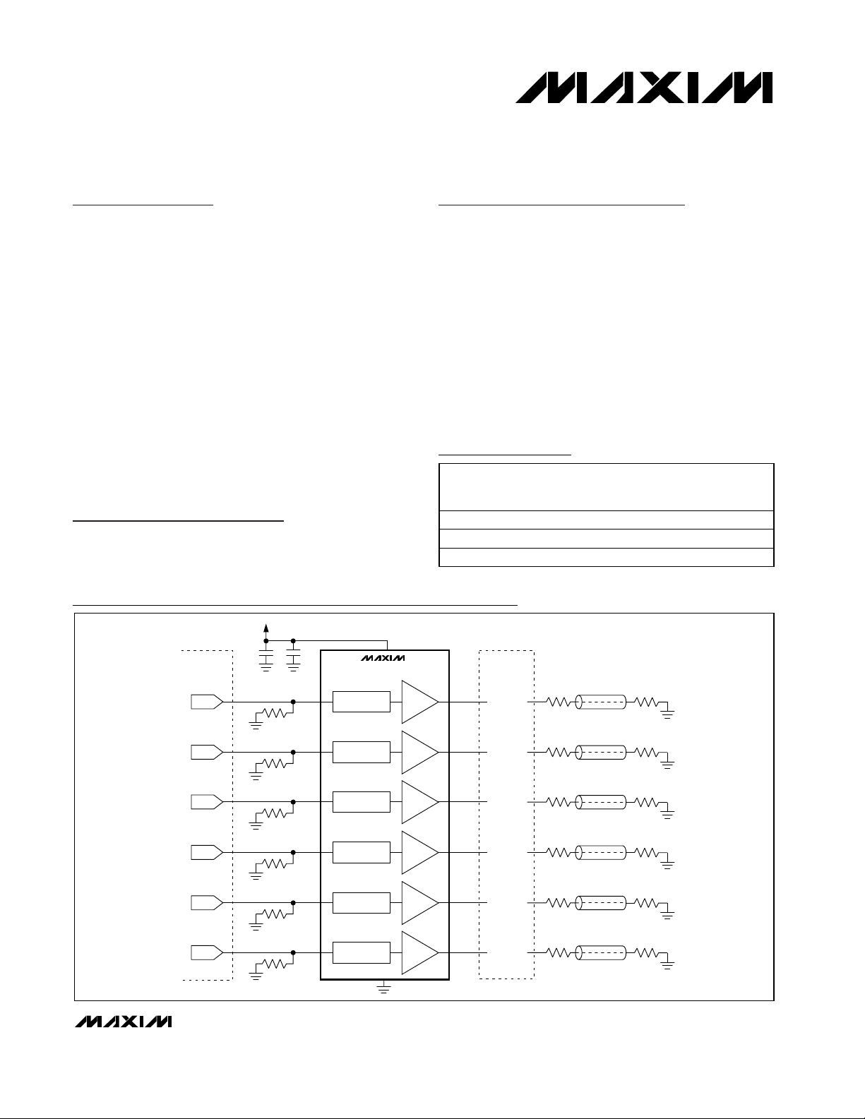
The MAX7440/MAX7441/MAX7442 six-channel video
reconstruction filters replace 30 or more discrete components. The devices are ideal for digital-to-analog
converter (DAC) video reconstruction applications,
when analog video is reconstructed from a digital data
stream. The MAX7440/MAX7441/MAX7442 operate
from a single +5V power supply. The inputs are DCcoupled from the DAC and the output can either be ACor DC-coupled. The DC-IN, DC-OUT architecture, leads
to a perfect line-time distortion performance (zero tilt).
The filters have a cutoff frequency optimized for PAL,
NTSC, and SDTV video applications and offer three
high-frequency boost options. The MAX7440 offers a
flat passband response on all six channels; the
MAX7441/MAX7442 offer high-frequency boost on the
three channels used for CVBS and Y/C. The MAX7440/
MAX7441/MAX7442 are available in a 14-pin SO package and are fully specified over the extended temperature range.
Applications
Features
♦ Replace 30 or More Discrete Components
♦ Ideal for CVBS, Y/C (S-Video), and RGB or Y Pb Pr
Applications
♦ 45dB Attenuation at 27MHz
♦ -0.2dB Passband Response
♦ Ideal for STBs with SCART Interface
♦ +5V Single-Supply Voltage
♦ Input Common-Mode Range Includes GND
♦ DC-Coupled Input, DC/AC-Coupled Output
♦ 14-Pin SO Package
MAX7440/MAX7441/MAX7442
6-Channel Integrated Video Reconstruction
Filters
________________________________________________________________ Maxim Integrated Products 1
Ordering Information
19-2750; Rev 0; 1/03
For pricing, delivery, and ordering information, please contact Maxim/Dallas Direct! at
1-888-629-4642, or visit Maxim’s website at www.maxim-ic.com.
*Future product—contact factory for availability.
75Ω
75Ω
A/V SWITCHING
DEVICE (MAX4399)
OR BUFFERS
OUT1
IN1
+5V
0.1µF1µF
LOWPASS FILTER
WITH HF BOOST*
A = +1V/V
D/A
ENCODER
75Ω
OUT2
IN2
LOWPASS FILTER
A = +1V/V
D/A
75Ω
OUT3
IN3
LOWPASS FILTER
A = +1V/V
D/A
75Ω
OUT4
IN4
LOWPASS FILTER
A = +1V/V
D/A
75Ω
OUT5
IN5
LOWPASS FILTER
WITH HF BOOST*
A = +1V/V
D/A
75Ω
OUT6
*MAX7440 HAS FLAT RESPONSE, MAX7441/MAX7442 INCLUDES HF BOOST.
IN6
LOWPASS FILTER
WITH HF BOOST*
A = +1V/V
D/A
75Ω
75Ω
75Ω
75Ω
75Ω
MAX7440
MAX7441
MAX7442
Typical Application Circuit
STB
DVDs
Hard Disk Recorders
PVR
SCART Video Applications
General Video Filtering
PART TEMP RANGE
MAX7440ESD -40°C to +85°C 14 SO No
MAX7441ESD -40°C to +85°C 14 SO Yes
MAX7442ESD* -40°C to +85°C 14 SO Yes
PINPACKAGE
H IG H -
F R EQ U EN C Y
B O O ST
Page 2
MAX7440/MAX7441/MAX7442
6-Channel Integrated Video Reconstruction
Filters
2 _______________________________________________________________________________________
ABSOLUTE MAXIMUM RATINGS
ELECTRICAL CHARACTERISTICS
(VCC= +5V ±5%, RL= 5kΩ, CL= 0 to 20pF, TA= T
MIN
to T
MAX
, unless otherwise noted. Typical values are at TA= +25°C.)
Stresses beyond those listed under “Absolute Maximum Ratings” may cause permanent damage to the device. These are stress ratings only, and functional
operation of the device at these or any other conditions beyond those indicated in the operational sections of the specifications is not implied. Exposure to
absolute maximum rating conditions for extended periods may affect device reliability.
VCCto GND ...........................................................................+6V
All Other Pins to GND.................................-0.3V to (V
CC
+ 0.3V)
Maximum Current into Any Pin .........................................±50mA
Continuous Power Dissipation (T
A
= +70°C)
14-Pin SO (derate 8.3mW/°C above +70°C)..............666.7mW
Operating Temperature Range ...........................-40°C to +85°C
Storage Temperature Range .............................-65°C to +150°C
Junction Temperature......................................................+150°C
Lead Temperature (soldering, 10s) .................................+300°C
Passband Response
Stopband Attenuation A
Boost Amplitude f = 4.5MHz
Differential Gain dG 5-step modulated staircase 0.05 %
Differential Phase dB 5-step modulated staircase 0.05 Degrees
Signal-to-Noise Ratio SNR
Group Delay Matching tg(MATCH)
Group Delay Deviation ∆
Line-Time Distortion H
Field-Time Distortion V
Low-Frequency Gain Variation A
Low-Frequency Gain 0.975 V/V
Low-Frequency Gain Matching t
Input Voltage Range 0 1.75 V
Channel-to-Channel Crosstalk X
Input Leakage Current I
PARAMETER SYMBOL CONDITIONS MIN TYP MAX UNITS
sb
g
dist
dist
V
g
TALK
IN
DC to 3.5MHz, MAX7440/MAX7441
(channels 2, 3, 4)
DC to 5MHz, MAX7440/MAX7441
(channels 2, 3, 4)
f = 27MHz 37 45 dB
Peak signal (1V
to 100MHz
Low-frequency
channel-to-channel
matching,
f = 200kHz
Deviation from
100kHz to 4.5MHz
18µs, 100IRE bar -3 0 +3 mV
130 lines, 18µs, 100IRE bar -4 +4 mV
Gain at f = 100kHz -0.25 +0.25 dB
f = 100kHz -3 +3 %
Channel-to-channel crosstalk, DC to 5MHz 71 dB
VIN = 0V 2 6 25 µA
-0.40 -0.2 +0.10
-0.80 -0.5 0
+1dB HF boost,
MAX7441
+2dB HF boost,
MAX7442
) to RMS noise, f = 10Hz
P-P
Channels 2, 3, 4 2
Channels 1, 5, 6 2
MAX7440/MAX7441/
MAX7442
MAX7441 (channels
1, 5, 6)
MAX7442 (channels
1, 5, 6)
0.4 0.60 0.91
1.2
71 dB
10
17
17
dB
dB
ns
ns
Page 3
MAX7440/MAX7441/MAX7442
6-Channel Integrated Video Reconstruction
Filters
_______________________________________________________________________________________ 3
ELECTRICAL CHARACTERISTICS (continued)
(VCC= +5V ±5%, RL= 5kΩ, CL= 0 to 20pF, TA= T
MIN
to T
MAX
, unless otherwise noted. Typical values are at TA= +25°C.)
0
-70
0.1 1 10 100
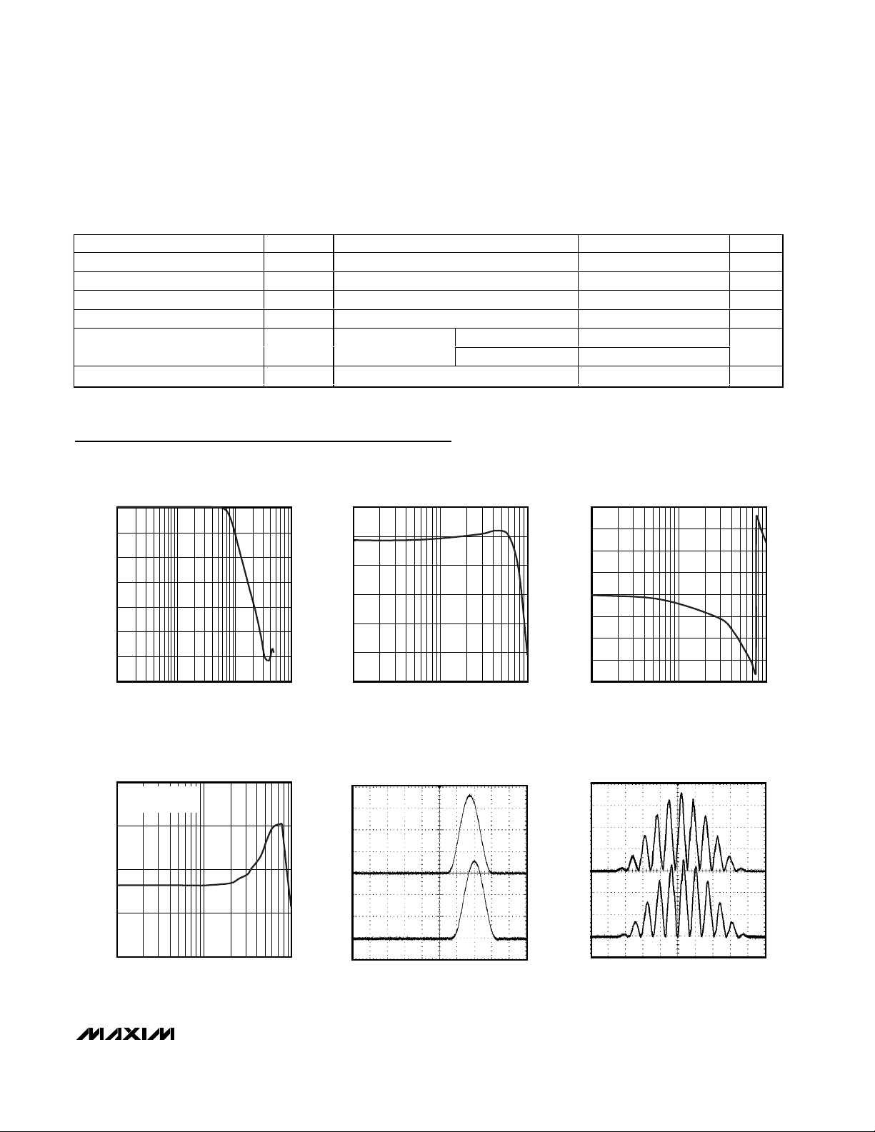
AMPLITUDE vs. FREQUENCY
-50
-60
MAX7440 toc01
FREQUENCY (MHz)
AMPLITUDE (dB)
-40
-30
-20
-10
PASSBAND AMPLITUDE vs. FREQUENCY
MAX7440 toc02
FREQUENCY (MHz)
AMPLITUDE (dB)
1
-8
-6
-4
-2
0
2
-10
0.1 10
PHASE RESPONSE vs. FREQUENCY
MAX7440 toc03
FREQUENCY (MHz)
PHASE (DEGREES)
1
-150
-100
-50
0
50
100
150
200
-200
0.1 10
80
40
0.1 1 10
GROUP DELAY vs. FREQUENCY
50
MAX7440toc04
FREQUENCY (MHz)
GROUP DELAY (ns)
60
70
MAX7441
(CHANNELS 2, 3, 4)
200ns/div
2T RESPONSE (1IRE = 7.14mV)
IN_
200mV/div
MAX7440 toc05
OUT_
200mV/div
400ns/div
MODULATED 12.5T RESPONSE
(1IRE = 7.14mV)
IN_
200mV/div
MAX7440 toc06
OUT_
200mV/div
Typical Operating Characteristics
(VCC= +5V, RL= 5kΩ, TA= +25°C, unless otherwise noted.)
PARAMETER SYMBOL CONDITIONS MIN TYP MAX UNITS
Input Resistance 200 kΩ
Input Capacitance 20 pF
Supply Voltage Range V
Supply Current I
CC
CC
Power-Supply Rejection Ratio PSRR VIN = 100mV
DC Level Shift OUT_ to IN_ 0.85 1.05 V
4.75 5.25 V
VCC = +5.5V, no load 57 78 mA
P-P
DC 39
f = 0 to 1MHz 30
dB
Page 4

MAX7440/MAX7441/MAX7442
6-Channel Integrated Video Reconstruction
Filters
4 _______________________________________________________________________________________
Typical Operating Characteristics (continued)
(VCC= +5V, RL= 5kΩ, TA= +25°C, unless otherwise noted.)
50
54
52
58
56
60
62
-40 10-15 35 60 85
SUPPLY CURRENT
vs. TEMPERATURE
MAX7440 toc07
TEMPERATURE (°C)
SUPPLY CURRENT (mA)
0
10
30
20
40
50
1.8 2.12.0 2.21.9 2.3
2.4
2.5
GROUP DELAY MATCHING DISTRIBUTION
MAX7440 toc11
GROUP DELAY (ns)
PERCENTAGE OF UNITS (%)
20 SAMPLES
-65
-90
0.1 1 10
CHANNEL-TO-CHANNEL CROSSTALK
vs. FREQUENCY
-85
MAX7440toc10
FREQUENCY (MHz)
AMPLITUDE (dB)
-75
-80
-70
0.3
0.2
0.1
0
-0.1
-0.2
-0.3
DIFFERENTIAL GAIN (%)
1324567
DIFFERENTIAL PHASE
DIFFERENTIAL GAIN
0.3
0.2
0.1
0
-0.1
(DEGREES)
-0.2
-0.3
DIFFERENTIAL PHASE
1324567
SIGNAL SWING vs. LOAD
4.5
4.0
MAX7440 toc08
3.5
)
P-P
3.0
2.5
2.0
SIGNAL SWING (V
1.5
1.0
0.5
200 18001000 2600 3400 4200 5000
LOAD (Ω)
INPUT/OUTPUT LEVEL SHIFT
vs. TEMPERATURE
950
910
870
MAX7440 toc09
MAX7440 toc12
OUT_
200mV/div
MULTIBURST RESPONSE
10µs/div
MAX7440 toc13
830
LEVEL SHIFT (mV)
790
750
-40 10-15 35 60 85
TEMPERATURE (°C)
Page 5

MAX7440/MAX7441/MAX7442
6-Channel Integrated Video Reconstruction
Filters
_______________________________________________________________________________________ 5
Pin Description
Detailed Description
The MAX7440/MAX7441/MAX7442 filter the outputs of
DAC encoder chipsets that process digital video information in applications such as set-top boxes, hard disk
recorders, DVD players, DVD recorders, and digital
VCRs. These devices also filter and clean up analog
video signals by rejecting out-of-band noise. Each
channel in the MAX7440/MAX7441/MAX7442 includes
a 4th-order lowpass filter and a gain of +1V/V output
stage, as shown in the Typical Application Circuit.
Filter
Filter Response
Each channel of the reconstruction filter consists of a
4th-order Sallen-Key filter configured as two 2nd-order
stages. The filter features a maximally flat passband for
NTSC, PAL, and SDTV bandwidths. The stopband
offers typically 45dB of attenuation at sampling frequencies of 27MHz and above (see Typical Operating
Characteristics). The filter exhibits a Butterworth-type
response resulting in excellent group delay deviation
performance.
High-Frequency Boost
The high-frequency (HF) boost compensates for signal
degradation and rolloff in the signal path prior to the filter. This performance increases the image sharpness.
The MAX7441/MAX7442 offer a high-frequency boost
on channels OUT1, OUT5, and OUT6.
Output Stage
The output stages of the MAX7440/MAX7441/MAX7442
are designed to drive 1V
P-P
signals into high-impedance (>5kΩ) loads. They require external buffers to
drive standard video cables. Most standard audio/
video switching devices include these buffers for STB
applications.
Applications Information
MAX7440/MAX7441/MAX7442 with an A/V
Switching Device
The MAX7440/MAX7441/MAX7442 are designed to
directly interface to an audio/video switching device
used in video applications (i.e., STBs) with SCART
interfaces (see Typical Application Circuit). The output
of the analog filters can drive the high-impedance load
of the switching device. The switching device provides
the buffering to drive standard 150Ω video loads.
MAX7440/MAX7441/MAX7442 with
External Buffers
External buffering is required for the MAX7440/
MAX7441/MAX7442 to drive standard 150Ω video
loads. Figure 1 shows the MAX4394 triple op amp, configured with a gain of +2V/V to drive standard video
loads from the MAX7440/MAX7441/MAX7442.
PIN NAME FUNCTION
1 IN1 Channel 1 Filter Input (Optional Boosted Channel)
2 IN2 Channel 2 Filter Input
3 IN3 Channel 3 Filter Input
4VCC+5V Power Supply. Bypass to GND with a 0.1µF and 1µF capacitor.
5 IN4 Channel 4 Filter Input
6 IN5 Channel 5 Filter Input (Optional Boosted Channel)
7 IN6 Channel 6 Filter Input (Optional Boosted Channel)
8 OUT6 Channel 6 Filter Output
9 OUT5 Channel 5 Filter Output
10 OUT4 Channel 4 Filter Output
11 GND Ground
12 OUT3 Channel 3 Filter Output
13 OUT2 Channel 2 Filter Output
14 OUT1 Channel 1 Filter Output
Page 6

MAX7440/MAX7441/MAX7442
Power-Supply Bypassing and Layout
The MAX7440/MAX7441/MAX7442 operate from a single +5V supply. Bypass VCCto GND with a 0.1µF and
1µF capacitor. These capacitors filter all frequencies
over 1MHz. Place all external components as close to
the devices as possible. To maintain good crosstalk
performance ensure that input and output lines do not
run parallel for any distance. If it is necessary to have
parallel lines, run a ground trace in between each line.
Refer to the MAX7440 Evaluation Kit for a proven PC
board layout example.
Chip Information
TRANSISTOR COUNT: 3691
PROCESS: BiCMOS
6-Channel Integrated Video Reconstruction
Filters
6 _______________________________________________________________________________________
Figure 1. Typical Application Circuit with External Buffers
Pin Configuration
V
+5V
CC
0.1µF1µF
ENCODER
MAX7440
MAX7441
MAX7442
D/A
D/A
IN1
IN6
LOWPASS FILTER
LOWPASS FILTER
A = +1V/V
A = +1V/V
OUT1 IN
OUT6
510Ω
IN
510Ω
DISABLE
MAX4394
510Ω
DISABLE
MAX4394
510Ω
75Ω
75Ω
Z
Z
= 75Ω
O
= 75Ω
O
OUT1
75Ω
OUT6
75Ω
TOP VIEW
IN1
IN2
IN3
IN4
IN5
1
2
3
4
5
6
7
MAX7440
MAX7441
MAX7442
CC
14
OUT1
13
OUT2
12
OUT3
11
GNDV
OUT4
10
9
OUT5
OUT6IN6
8
SO
Page 7

MAX7440/MAX7441/MAX7442
6-Channel Integrated Video Reconstruction
Filters
Maxim cannot assume responsibility for use of any circuitry other than circuitry entirely embodied in a Maxim product. No circuit patent licenses are
implied. Maxim reserves the right to change the circuitry and specifications without notice at any time.
7 _____________________Maxim Integrated Products, 120 San Gabriel Drive, Sunnyvale, CA 94086 408-737-7600
© 2003 Maxim Integrated Products Printed USA is a registered trademark of Maxim Integrated Products.
Package Information
(The package drawing(s) in this data sheet may not reflect the most current specifications. For the latest package outline information
go to www.maxim-ic.com/packages
.)
N
1
TOP VIEW
D
e
FRONT VIEW
INCHES
DIM
MIN
0.053A
0.004
A1
0.014
B
0.007
C
e 0.050 BSC 1.27 BSC
0.150
HE
A
B
A1
C
L
E
H 0.2440.228 5.80 6.20
0.016L
VARIATIONS:
INCHES
MINDIM
D
0.189 0.197 AA5.004.80 8
0.337 0.344 AB8.758.55 14
D
0-8
SIDE VIEW
MAX
0.069
0.010
0.019
0.010
0.157
0.050
MAX
0.3940.386D
MILLIMETERS
MAX
MIN
1.35
1.75
0.10
0.25
0.35
0.49
0.19
0.25
3.80 4.00
0.40 1.27
MILLIMETERS
MAX
MIN
9.80 10.00
N MS012
16
AC
SOICN .EPS
PROPRIETARY INFORMATION
TITLE:
PACKAGE OUTLINE, .150" SOIC
REV.DOCUMENT CONTROL NO.APPROVAL
21-0041
1
B
1
 Loading...