

Page 1
General Description
The MAX7438/MAX7439 three-channel standard definition video reconstruction filters include a back-porch
clamp that sets the output blanking level of the video
signal to ground. Each channel of the MAX7438/
MAX7439 combines a lowpass filter with adjustable
high-frequency boost levels and an output buffer capable of driving two standard 150Ω video loads. The
blanking level of the output video signal on each channel is clamped to ground, eliminating the need for large
AC-coupling output capacitors. Direct input coupling
circuitry eliminates the need for AC-coupling input
capacitors. This DC-in/DC-out architecture results in
extremely low line-time distortion. The MAX7438/
MAX7439 are ideal for antialiasing and DAC smoothing
in digital video devices such as STBs, DVDs, PVRs,
and hard disk recorders. The MAX7438/MAX7439 operate from ±5V dual supplies.
The three-channel MAX7438/MAX7439 are ideal for Y,
Pb, Pr, and RGB component video signals, three composite video signals, and also Y/C plus CVBS video signals. Each filter channel achieves 60dB of attenuation at
27MHz and a maximally flat passband from DC to 5MHz.
The MAX7438 offers an internal gain of +2V/V, while the
MAX7439 offers a gain of +3V/V.
Applications
Features
♦ Back-Porch of Video Output Signal Clamped to
Ground
♦ Eliminates Input/Output AC-Coupling Capacitors
♦ 0.1% Line-Time Distortion
♦ Stopband: 55dB at 27MHz
♦ Passband: ±0.8dB out to 5MHz
♦ Diff Gain = 0.05%, Diff Phase = 0.05 Degrees
♦ Output Clamped to Ground with Loss of Input
♦ Each Output Drives Two 150Ω Video Loads
♦ Up to 2dB of High-Frequency Boost Control
♦ Ideal for CVBS, Y/C (S-Video), and RGB (Y, P
b,Pr
)
Outputs for NTSC, PAL, and SDTV
♦ Filter Bypass Mode
♦ Small 20-Pin 5mm
✕
5mm Thin QFN Package
MAX7438/MAX7439
Triple-Channel Video Reconstruction Filters with
Back-Porch Clamp to GND
________________________________________________________________ Maxim Integrated Products 1
Ordering Information
19-2857; Rev 0; 4/03
For pricing, delivery, and ordering information, please contact Maxim/Dallas Direct! at
1-888-629-4642, or visit Maxim’s website at www.maxim-ic.com.
*EP = Exposed paddle
Pin Configuration appears at end of data sheet.
EVALUATION KIT
AVAILABLE
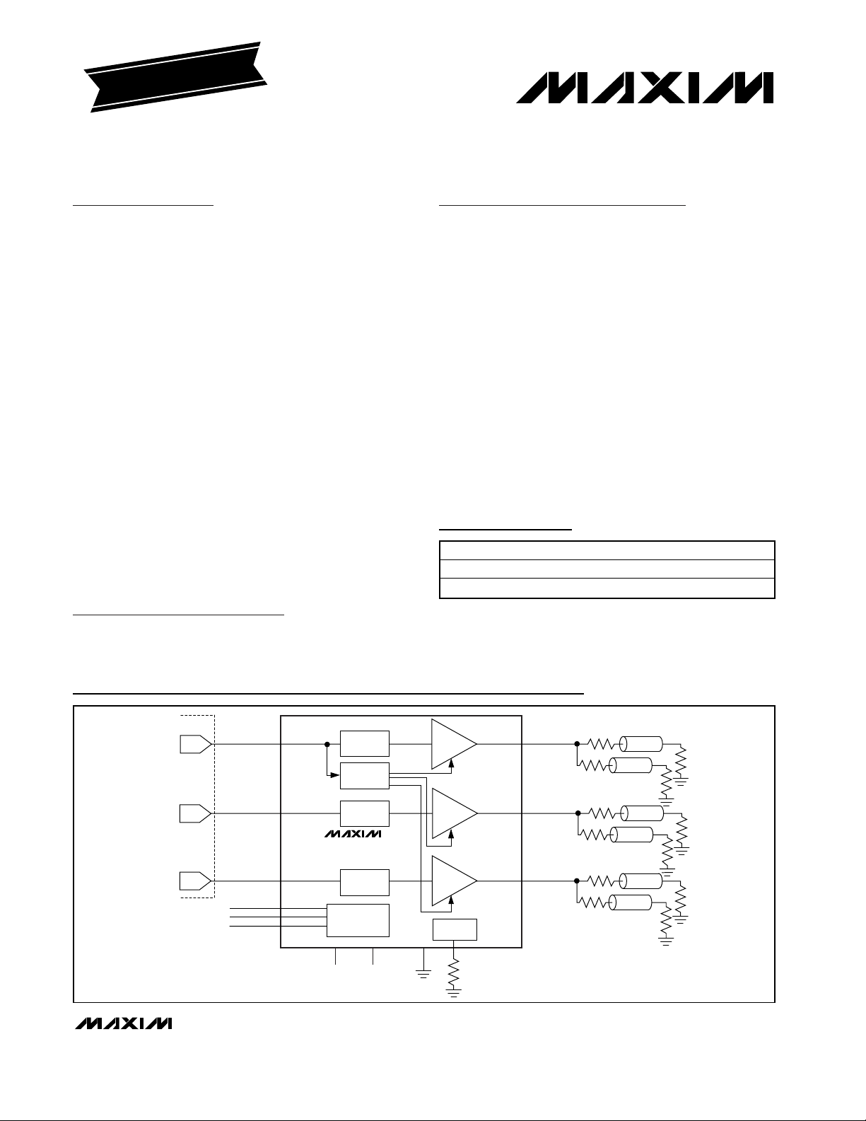
Functional Diagram
Set-Top Boxes/HDR/DVD
Game Consoles
Camcorders
Composite, Component,
S-Video Output for
NTSC, PAL, SDTV
PART TEMP RANGE PIN-PACKAGE
MAX7438ETP -40°C to +85°C 20 Thin QFN-EP*
MAX7439ETP -40°C to +85°C 20 Thin QFN-EP*
ENCODER
IN1
DAC1
IN2
DAC2
IN3
DAC3
HFB1
HFB2
HFB3
LOWPASS
FILTER
BACK-PORCH
DETECTOR
LOWPASS
FILTER
MAX7438
MAX7439
LOWPASS
FILTER
HIGH-FREQUENCY
BOOST CONTROL/
BYPASS
V
= -5VV
= +5V
SS
CC
75Ω
GAIN/LEVEL
SHIFT
GAIN/LEVEL
SHIFT
GAIN/LEVEL
SHIFT
GENERATOR
GND
BIAS
EXT
10kΩ
OUT1
OUT2
OUT3
75Ω
75Ω
75Ω
75Ω
75Ω
Z0 = 75Ω
Z0 = 75Ω
75Ω
Z0 = 75Ω
Z0 = 75Ω
75Ω
Z0 = 75Ω
Z0 = 75Ω
75Ω
75Ω
75Ω
75Ω
Page 2
MAX7438/MAX7439
Triple-Channel Video Reconstruction Filters with
Back-Porch Clamp to GND
2 _______________________________________________________________________________________
ABSOLUTE MAXIMUM RATINGS
Stresses beyond those listed under “Absolute Maximum Ratings” may cause permanent damage to the device. These are stress ratings only, and functional
operation of the device at these or any other conditions beyond those indicated in the operational sections of the specifications is not implied. Exposure to
absolute maximum rating conditions for extended periods may affect device reliability.
VCCto GND..............................................................-0.3V to +6V
V
SS
to GND...............................................................-6V to +0.3V
OUT_ to GND ........................................................-2.5V to +3.5V
All Other Pins to GND ......................(V
SS
- 0.3V) to (VCC+ 0.3V)
Maximum Current into Any Pin .........................................±50mA
Continuous Power Dissipation (T
A
= +70°C)
20-Pin 5mm x 5mm Thin QFN (derate 20.8mW/°C
above +70°C)...........................................................1666.7mW
Operating Temperature Range ...........................-40°C to +85°C
Storage Temperature Range .............................-65°C to +150°C
Junction Temperature......................................................+150°C
Lead Temperature (soldering, 10s) .................................+300°C
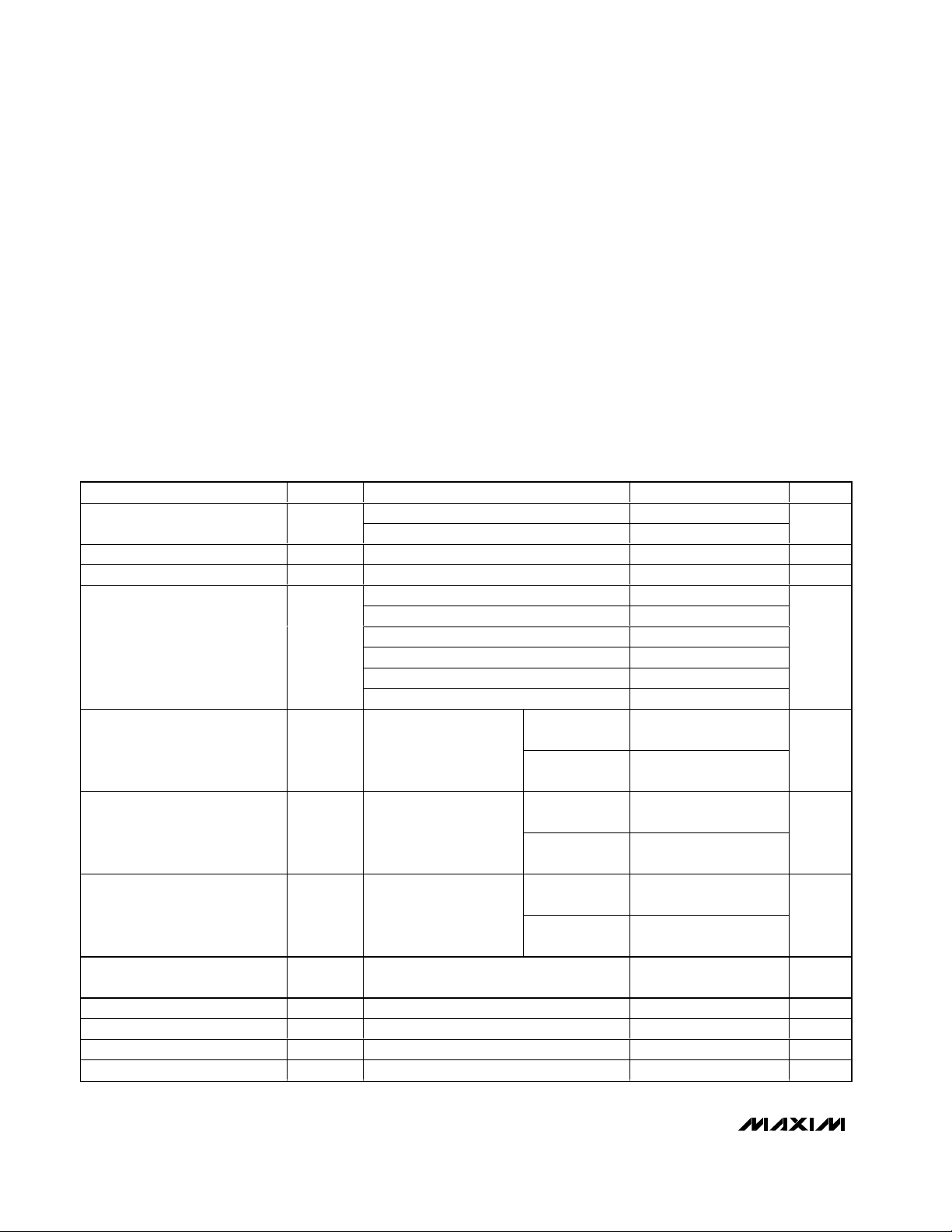
ELECTRICAL CHARACTERISTICS
(VCC= +5V ±5%, VSS= -5V ±5%, R
EXT
= 10kΩ ±1%, R
HFB_-1
= 15kΩ ±1%, R
HFB_-2
= 1kΩ ±1%, no boost, R
OUT
= 75Ω,
C
OUT
= 0 to 20pF, TA= T
MIN
to T
MAX
, unless otherwise noted. Typical values are at TA= +25°C.)
)
PARAMETER SYMBOL CONDITIONS MIN TYP MAX UNITS
Passband Response
Stopband Attenuation A
HF Boost Step Size f = 4.2MHz 0.45 dB
HFB_ Voltage Range V
Differential Gain dG
Differential Phase dθ
Total Harmonic Distortion THD
Signal-to-Noise Ratio SNR
Group Delay Deviation ∆t
Group Delay Matching t
Line-Time Distortion H
Field-Time Distortion V
f = 100kHz to 4.2MHz, no HF boost -0.6 +0.6
f = 100kHz to 5MHz, no HF boost -0.8 +0.8
f = 27MHz, relative to 100kHz 40 60 dB
SB
Bypass 0 50
No boost 280 360
HFB_
Boost 1 670 850
Boost 2 1360 1700
Boost 3 2250 2750
Boost 4 3500 V
5-step modulated
staircase
5-step modulated
staircase
f = 100kHz to 5MHz,
= 0.7V
V
IN
P-P
Output signal (2V
f = 100Hz to 5MHz
Deviation from 100kHz to 3.58(4.43)MHz 12 30 ns
G
G(MATCH
DIST
DIST
f = 100kHz 2 ns
18µs, 100 IRE bar 0.1 %
130 lines, 18µs, 100 IRE bar 0.2 %
P-P
MAX7438,
= 1V
V
IN
MAX7439,
= 670mV
V
IN
MAX7438,
= 1V
V
IN
MAX7439,
= 670mV
V
IN
MAX7438,
= 700mV
V
IN
MAX7439,
= 460mV
V
IN
) to P-P noise,
P-P
P-P
P-P
P-P
P-P
P-P
68 75 dB
0.05 0.5
0.05 0.5
0.05 0.5
0.05 0.5
0.2 0.5
0.2 0.5
CC
dB
mV
%
Degrees
%
Page 3
MAX7438/MAX7439
Triple-Channel Video Reconstruction Filters with
Back-Porch Clamp to GND
_______________________________________________________________________________________ 3
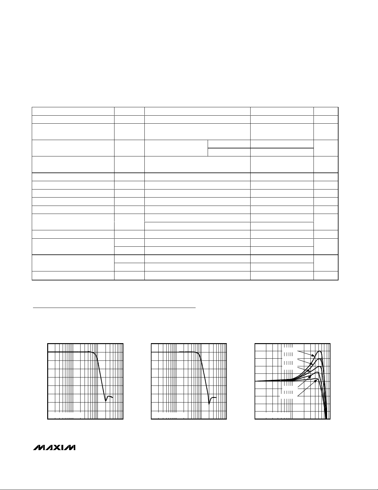
ELECTRICAL CHARACTERISTICS (continued)
(VCC= +5V ±5%, VSS= -5V ±5%, R
EXT
= 10kΩ ±1%, R
HFB_-1
= 15kΩ ±1%, R
HFB_-2
= 1kΩ ±1%, no boost, R
OUT
= 75Ω,
C
OUT
= 0 to 20pF, TA= T
MIN
to T
MAX
, unless otherwise noted. Typical values are at TA= +25°C.)
Typical Operating Characteristics
(VCC= +5V, VSS= -5V, R
OUT_
= 150Ω, R
EXT
= 10kΩ, no boost, TA= +25°C, unless otherwise noted.)
-80
0.1 100101
MAX7438
AMPLITUDE vs. FREQUENCY
-50
-70
-10
-30
10
-40
-60
0
-20
MAX7438/9 toc01
FREQUENCY (MHz)
GAIN (dB)
NORMALIZED TO 0dB
-80
0.1 100101
MAX7439
AMPLITUDE vs. FREQUENCY
-50
-70
-10
-30
10
-40
-60
0
-20
MAX7438/9 toc02
FREQUENCY (MHz)
GAIN (dB)
NORMALIZED TO 0dB
2.5
2.0
1.5
1.0
0.5
0
-0.5
-1.0
-1.5
-2.0
-2.5
0.1 1 10
MAX7438
PASSBAND AMPLITUDE vs. FREQUENCY
MAX7438/9 toc03
FREQUENCY (MHz)
GAIN (dB)
NORMALIZED TO 0dB
BOOST 4
BOOST 3
BOOST 2
NO BOOST
BOOST 1
PARAMETER SYMBOL CONDITIONS MIN TYP MAX UNITS
Clamp Accuracy Output blanking level relative to GND -55 +55 mV
Clamp Settling Time
Low-Frequency Gain Gain at 100kHz
Low-Frequency Gain Matching t
Input Voltage Range THD < 0.5% -0.5 +1.8 V
Output Voltage Range V
Channel-to-Channel Crosstalk X
Output Short-Circuit Current I
Input Leakage Current at IN_ I
Input Leakage Current at HFB_ I
Input Resistance 500 kΩ
Supply Voltage Range
Supply Current
Power-Supply Rejection Ratio PSRR VIN = 100mV
Back porch within the specified clamp
accuracy
MAX7438 5.5 6 6.5
MAX7439 9 9.54 10
Channel-to-channel gain matching,
G
f = 100kHz
OUT
TALK
SC
IN_
HFB_
V
V
I
CC
I
SS
f = 5MHz -0.8 +1.8 V
Channel-to-channel crosstalk, f = 5MHz -60 dB
OUT_ shorted to GND or V
CC
Bypass mode, boost 1 to boost 3 0.2
Boost 4 30
CC
SS
VCC = +5.25V, no load 110 160
VSS = -5.25V, no load 110 160
, f = 0 to 3.5MHz 30 dB
P-P
50 Lines
+5 %
50 mA
±1 ±5 µA
4.75 5.25
-4.75 -5.25
dB
µA
V
mA
Page 4
MAX7438/MAX7439
Triple-Channel Video Reconstruction Filters with
Back-Porch Clamp to GND
4 _______________________________________________________________________________________
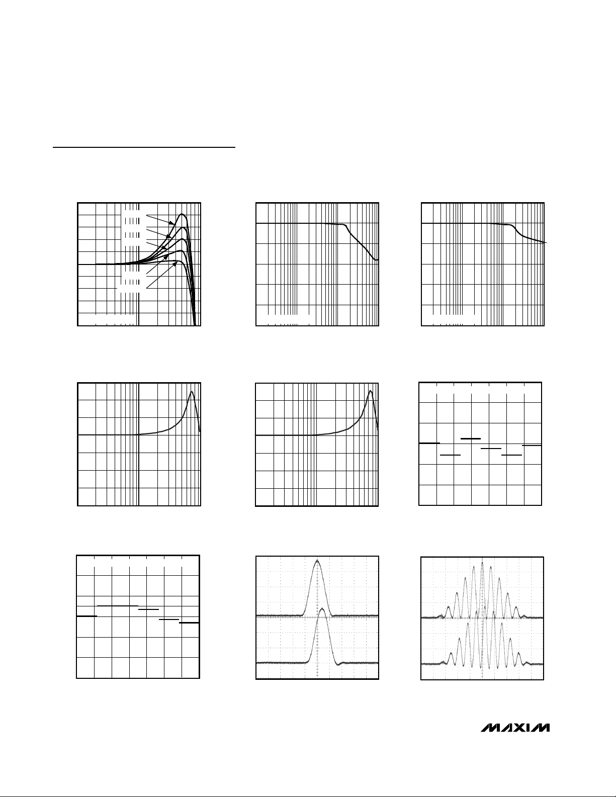
Typical Operating Characteristics (continued)
(VCC= +5V, VSS= -5V, R
OUT_
= 150Ω, R
EXT
= 10kΩ, no boost, TA= +25°C, unless otherwise noted.)
2.5
2.0
1.5
1.0
0.5
0
-0.5
-1.0
-1.5
-2.0
-2.5
0.1 1 10
MAX7439
PASSBAND AMPLITUDE vs. FREQUENCY
MAX7438/9 toc04
FREQUENCY (MHz)
GAIN (dB)
NORMALIZED TO 0dB
BOOST 4
BOOST 3
BOOST 2
NO BOOST
BOOST 1
-50
0.1 100101
MAX7438
CHANNEL RESPONSE (BYPASS MODE)
-30
-40
10
-20
0
-10
MAX7438/9 toc05
FREQUENCY (MHz)
GAIN (dB)
NORMALIZED TO 0dB
-50
0.1 100101
MAX7439
CHANNEL RESPONSE (BYPASS MODE)
-30
-40
10
-20
0
-10
MAX7438/9 toc06
FREQUENCY (MHz)
GAIN (dB)
NORMALIZED TO 0dB
140
120
80
100
40
60
20
0
0.1 1 10
MAX7438
GROUP DELAY vs. FREQUENCY
MAX7438/9 toc07
FREQUENCY (MHz)
GROUP DELAY (ns)
140
120
80
100
40
60
20
0
0.1 1 10
MAX7439
GROUP DELAY vs. FREQUENCY
MAX7438/9 toc08
FREQUENCY (MHz)
GROUP DELAY (ns)
-0.2
-0.3
1ST 2ND 3RD 4TH 5TH 6TH
DIFFERENTIAL GAIN
-0.1
0.0
0.1
0.2
0.3
DIFFERENTIAL GAIN (%)
MAX7438/9 toc09
0.00 -0.04 -0.040.01 -0.02 -0.01
-0.2
-0.3
1ST 2ND 3RD 4TH 5TH 6TH
DIFFERENTIAL PHASE
-0.1
0.0
0.1
0.2
0.3
DIFFERENTIAL PHASE (DEGREES)
MAX7438/9 toc10
0.00 0.03 -0.010.03 -0.02 -0.02
IN_
200mv/div
200ns/div
200mv/div
OUT_
2T RESPONSE
MAX7438/9 toc11
IN_
200mv/div
200mv/div
400ns/div
OUT_
12.5T RESPONSE
MAX7438/9 toc12
Page 5
MAX7438/MAX7439
Triple-Channel Video Reconstruction Filters with
Back-Porch Clamp to GND
_______________________________________________________________________________________ 5
Typical Operating Characteristics (continued)
(VCC= +5V, VSS= -5V, R
OUT_
= 150Ω, R
EXT
= 10kΩ, no boost, TA= +25°C, unless otherwise noted.)
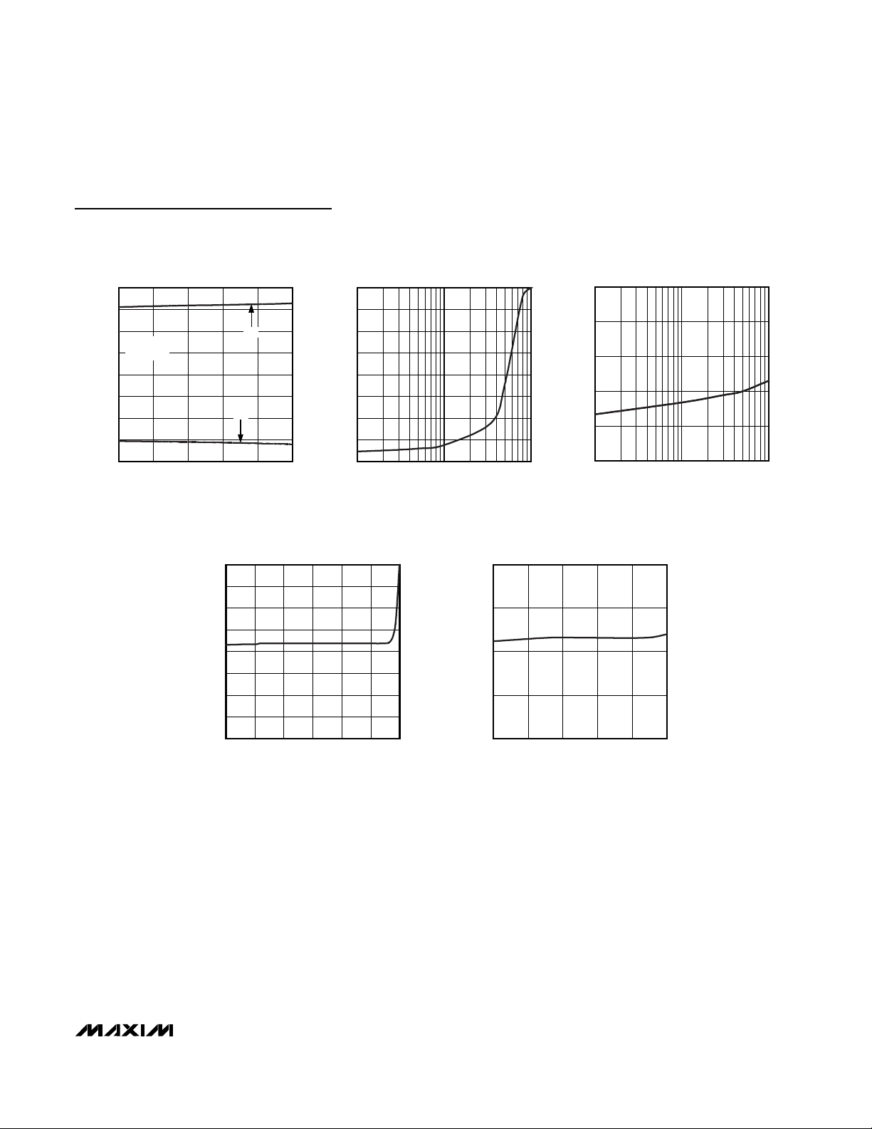
SUPPLY CURRENT VS. TEMPERATURE
140
105
70
VCC = +5V
35
= -5V
V
SS
0
-35
SUPPLY CURRENT (mA)
-70
-105
-140
-40 85
TEMPERATURE (°C)
100
75
50
25
-25
OUTPUT VOLTAGE (mV)
-50
-75
-100
I
CC
I
SS
6035-15 10
BACK-PORCH LEVEL OUTPUT VOLTAGE
vs. INPUT VOLTAGE
0
-0.2 1.6
OUTPUT SOURCE IMPEDANCE vs. FREQUENCY
4.0
3.5
MAX7438/9 toc13
3.0
2.5
2.0
1.5
OUTPUT IMPEDANCE (Ω)
1.0
0.5
0
0.1 10
1.31.00.1 0.4 0.7
INPUT VOLTAGE (V)
1
FREQUENCY (MHz)
MAX7438/9 toc16
PASSBAND CHANNEL-TO-CHANNEL
0
-20
MAX7438/9 toc14
-40
-60
CROSSTALK (dB)
-80
-100
BACK-PORCH CLAMP VOLTAGE
vs. TEMPERATURE
50
25
0
-25
BACK-PORCH CLAMP VOLTAGE (mV)
-50
-40 85
TEMPERATURE (°C)
CROSSTALK vs. FREQUENCY
MAX7438/9 toc15
10.1 10
FREQUENCY (MHz)
MAX7438/9 toc17
603510-15
Page 6

MAX7438/MAX7439
Detailed Description
Filter
Filter Response
The MAX7438/MAX7439 reconstruction filters consist of
three separate lowpass filters with Butterworth-type
response. The filter features a maximally flat passband
for NTSC and PAL bandwidths, while maintaining good
group delay characteristics. The stopband offers excellent attenuation at frequencies of 27MHz and above
(see the Typical Operating Characteristics section).
The autotrimming circuit digitally controls the corner frequency to maintain the frequency characteristics over
process and temperature.
High-Frequency Boost
The high-frequency boost compensates for signal
degradation and roll-off in the signal path prior to the
MAX7438/MAX7439 to increase image sharpness.
Program the level of high-frequency boost for each
channel by selecting the corresponding external resistor values (R
HFB_-1
and R
HFB_-2
, as shown in the
Typical Operating Circuit section) given in Table 1. The
Triple-Channel Video Reconstruction Filters with
Back-Porch Clamp to GND
6 _______________________________________________________________________________________
Pin Description
Table 1. External Resistor Values for Bypass Mode and High-Frequency Boost Control
PIN NAME FUNCTION
1, 4, 7, 10,
11, 13, 15, 19
2 IN1 Channel 1 Video Input
3 HFB1
5 OUT1 Channel 1 Video Output
6VCC+5V Power Input
8 OUT2 Channel 2 Video Output
9VSS-5V Power Input. Connect the backside exposed pad to VSS.
12 OUT3 Channel 3 Video Output
14 HFB3
16 IN3 Channel 3 Video Input
17 HFB2
18 IN2 Channel 2 Video Input
20 EXT External Bias Resistor. Connect a 10kΩ resistor from EXT to GND.
— EP Exposed Paddle. Connect to VSS. Do not connect to GND.
MODE
Bypass Open 0 0 Bypass Bypass
No boost 15 1 0.318 0 0
Boost 1 11.3 2 0.758 0.5 0.75
Boost 2 16.5 7.32 1.53 1.0 1.5
Boost 3 11.3 11.3 2.5 1.5 2.25
Boost 4 4.42 18.2 4.027 2.0 3.0
GND Ground
Channel 1 High-Frequency Boost and Filter Bypass Control Input. Connect external resistors to HFB1
for high-frequency boost and filter bypass control. See Table 1.
Channel 3 High-Frequency Boost and Filter Bypass Control Input. Connect external resistors to HFB3
for high-frequency boost and filter bypass control. See Table 1.
Channel 2 High-Frequency Boost and Filter Bypass Control Input. Connect external resistors to HFB2
for high-frequency boost and filter bypass control. See Table 1.
R
HFB_-1
(kΩ)
R
HFB_-2
(kΩ)
V
(V
HFB_
CC
(V)
= 5V)
NOMINAL BOOST (dB)/
BYPASS
(MAX7438)
NOMINAL BOOST (dB)/
BYPASS
(MAX7439)
Page 7
external resistors form a voltage-divider between V
CC
and GND. The values in the fourth column (V
HFB_
(V))
are calculated using the following equation:
V
HFB_
= VCCx R
HFB_-2
/ (R
HFB_-1
+ R
HFB_-2
)
where VCC= 5V.
Apply an external voltage to HFB_ in place of R
HFB_-1
and R
HFB_-2
as an alternative. See the Electrical
Characteristics section. Filter boost modes can also be
controlled from a microprocessor. See the Applications
Information section.
Filter Bypass
The MAX7438/MAX7439 offer selectable filter bypassing that allows any of the video inputs to be filtered or
unfiltered. Select the filter bypass mode for a given
channel by setting the corresponding values for
R
HFB_-1
and R
HFB_-2
according to Table 1.
Output Buffer
The output buffer is able to drive two standard 150Ω
video loads with a 2V
P-P
signal. The MAX7438 output
buffer has a preset gain of 2V/V, and the MAX7439 output buffer has a gain of 3V/V. The MAX7439 is ideal for
a DAC output whose voltage range is between 0.67V
and 1V. Set the DAC output to 0.67V to achieve a 2V/V
signal on OUT_.
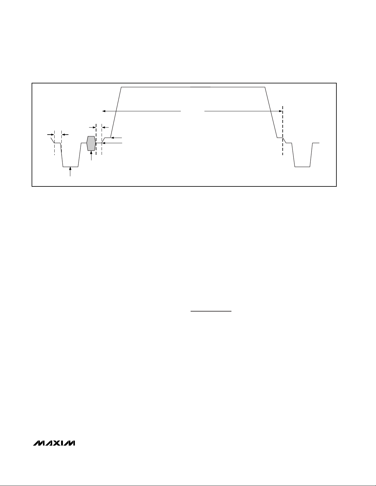
Back-Porch Clamp
The MAX7438/MAX7439 feature a back-porch clamp to
set the output blanking level. This clamp shifts the DC
level of the video signal so that the back-porch level is
close to ground (see Figure 1). The devices sense the
voltage during back porch and feed back into a control
system that provides the appropriate DC-level shift in
the filter channel to clamp the output to ground. The
back-porch clamp to ground eliminates the need for
large output-coupling capacitors that can introduce
unwanted line-time distortion (tilt), cost, and board
space. This feedback network and the on-chip capacitors introduce a finite settling time (50 lines max) after
power-up or any dramatic shift in input voltage (see the
Electrical Characteristics section).
Channel 1 requires a video signal with sync information
(CVBS, Y, or G), since the other two channels are
clamped from channel 1. In the absence of a sync on
channel 1, the circuit forces all outputs actively and
continuously to ground.
Applications Information
Power-Supply Bypassing and Layout
The MAX7438/MAX7439 operate from dual ±5V supplies. Bypass VCCand VSSto GND with 0.1µF capacitors in parallel with 1µF capacitors. Place the 0.1µF
capacitors as close to the power inputs as possible.
Since EXT is a sensitive input, place R
EXT
close to the
device to avoid signals coupling into EXT. Do not route
any input, output, or dynamic signal near this pin and
the accompanying trace.
Note: The exposed paddle is electrically connected to
VSS.
Do not connect the exposed paddle to ground. Refer to
the MAX7438 EV kit for layout examples, as well as a
proven PC board layout example.
MAX7438/MAX7439
Triple-Channel Video Reconstruction Filters with
Back-Porch Clamp to GND
_______________________________________________________________________________________ 7
Figure 1. Standard Video Signal
BACK
FRONT
PORCH
H-SYNC TIP
PORCH
COLOR BURST
BLACK LEVEL (SETUP)
BLANK LEVEL
ACTIVE VIDEO
Page 8
MAX7438/MAX7439
Microprocessor Control of High-Frequency
Boost and Bypass
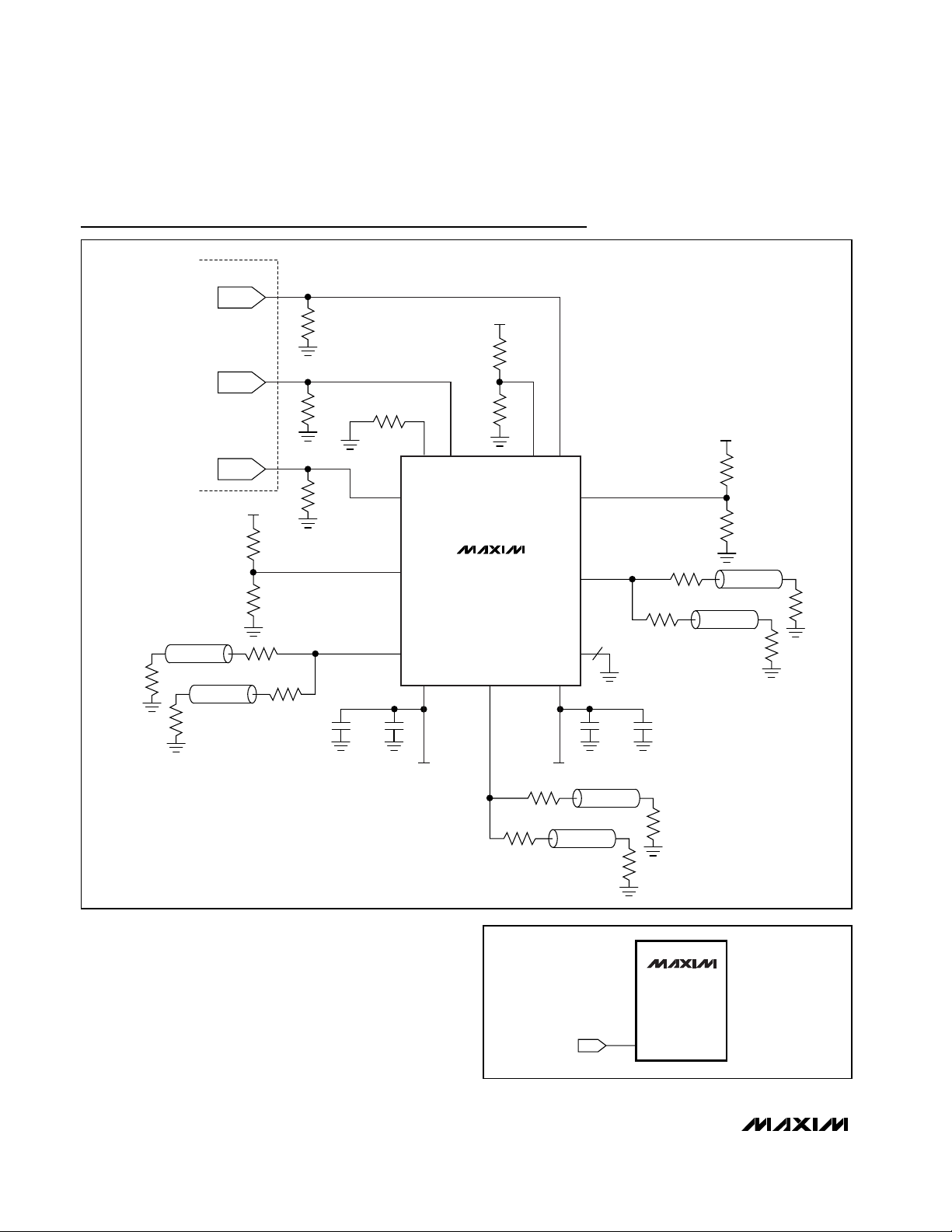
Use a DAC output to control the bypass and high-frequency boost levels on each channel (see Figure 2).
Set the DAC output voltage to the corresponding
bypass or boost levels desired (see Table 1).
Triple-Channel Video Reconstruction Filters with
Back-Porch Clamp to GND
8 _______________________________________________________________________________________
Typical Operating Circuit
Figure 2. DAC Control of High-Frequency Boost and Bypass
ENCODER
DAC3
V
R
R
HFB2-1
HFB2-2
CC
V
CC
DAC2
R
T
R
T
10kΩ
DAC1
R
V
CC
R
Z0 = 75Ω
75Ω
HFB1-1
R
HFB1-2
Z0 = 75Ω
75Ω
75Ω
T
75Ω
EXT IN2 HFB2 IN3
75Ω
75Ω
HFB3
OUT3
8
GND
V
SS
0.1µF 1µF
V
= -5V
SS
Z0 = 75Ω
Z0 = 75Ω
75Ω
75Ω
75Ω
75Ω
IN1
HFB1
OUT1
V
CC
0.1µF1µF
V
= +5V
CC
MAX7438
MAX7439
OUT2
Z0 = 75Ω
R
HFB3-1
R
HFB3-2
Z0 = 75Ω
75Ω
75Ω
MAX7438
MAX7439
DAC
HFB_
Page 9

MAX7438/MAX7439
Triple-Channel Video Reconstruction Filters with
Back-Porch Clamp to GND
_______________________________________________________________________________________ 9
Chip Information
TRANSISTOR COUNT: 6418
PROCESS: BiCMOS
20
19
18
17
EXT
GND
IN2
HFB2
16 IN3
13
12
11
14
15
OUT3
*CONNECT EXPOSED
PADDLE TO
V
SS
GND
HFB3
GND
GND
4
3
2
1
GND
HFB1
IN1
GND
5OUT1
6
7
8
9
V
CC
GND
OUT2
V
SS
10GND
TOP VIEW
5mm
✕
5mm THIN QFN
MAX7438
MAX7439
Pin Configuration
Page 10
MAX7438/MAX7439
Triple-Channel Video Reconstruction Filters with
Back-Porch Clamp to GND
Maxim cannot assume responsibility for use of any circuitry other than circuitry entirely embodied in a Maxim product. No circuit patent licenses are
implied. Maxim reserves the right to change the circuitry and specifications without notice at any time.
10 ____________________Maxim Integrated Products, 120 San Gabriel Drive, Sunnyvale, CA 94086 408-737-7600
© 2003 Maxim Integrated Products Printed USA is a registered trademark of Maxim Integrated Products.
Package Information
(The package drawing(s) in this data sheet may not reflect the most current specifications. For the latest package outline information,
go to www.maxim-ic.com/packages
.)
D
PIN # 1
I.D.
D/2
C
COMMON DIMENSIONS
A1
0.15 C A
E/2
A3
D2
b
0.10 M
PIN # 1 I.D.
0.35x45
E2/2
k
L
21-0140
C A B
QFN THIN.EPS
C
E2
L
CC
L
L
REV.
1
C
2
C
L
D2/2
0.15
C B
E
0.10
C
A
0.08 C
(NE-1) X e
DETAIL A
k
e
(ND-1) X e
L
L
e e
PROPRIETARY INFORMATION
TITLE:
PACKAGE OUTLINE
16, 20, 28, 32L, QFN THIN, 5x5x0.8 mm
APPROVAL
DOCUMENT CONTROL NO.
EXPOSED PAD VARIATIONS
NOTES:
1. DIMENSIONING & TOLERANCING CONFORM TO ASME Y14.5M-1994.
2. ALL DIMENSIONS ARE IN MILLIMETERS. ANGLES ARE IN DEGREES.
3. N IS THE TOTAL NUMBER OF TERMINALS.
4. THE TERMINAL #1 IDENTIFIER AND TERMINAL NUMBERING CONVENTION SHALL CONFORM TO JESD 95-1
SPP-012. DETAILS OF TERMINAL #1 IDENTIFIER ARE OPTIONAL, BUT MUST BE LOCATED WITHIN THE
ZONE INDICATED. THE TERMINAL #1 IDENTIFIER MAY BE EITHER A MOLD OR MARKED FEATURE.
5. DIMENSION b APPLIES TO METALLIZED TERMINAL AND IS MEASURED BETWEEN 0.25 mm AND 0.30 mm
FROM TERMINAL TIP.
6. ND AND NE REFER TO THE NUMBER OF TERMINALS ON EACH D AND E SIDE RESPECTIVELY.
7. DEPOPULATION IS POSSIBLE IN A SYMMETRICAL FASHION.
8. COPLANARITY APPLIES TO THE EXPOSED HEAT SINK SLUG AS WELL AS THE TERMINALS.
9. DRAWING CONFORMS TO JEDEC MO220.
10. WARPAGE SHALL NOT EXCEED 0.10 mm.
PROPRIETARY INFORMATION
TITLE:
PACKAGE OUTLINE
16, 20, 28, 32L, QFN THIN, 5x5x0.8 mm
21-0140
REV.DOCUMENT CONTROL NO.APPROVAL
2
C
2
 Loading...