

Page 1
For price, delivery, and to place orders, please contact Maxim Distribution at 1-888-629-4642,
or visit Maxim’s website at www.maxim-ic.com.
General Description
The MAX7418–MAX7425 5th-order, low-pass, switchedcapacitor filters (SCFs) operate from a single +5V
(MAX7418–MAX7421) or +3V (MAX7422–MAX7425)
supply. These devices draw only 3mA of supply current
and allow corner frequencies from 1Hz to 45kHz, making them ideal for low-power post-DAC filtering and antialiasing applications. They feature a shutdown mode
that reduces supply current to 0.2µA.
Two clocking options are available: self-clocking
(through the use of an external capacitor), or external
clocking for tighter corner-frequency control. An offset
adjust pin allows for adjustment of the DC output level.
The MAX7418/MAX7422 deliver 53dB of stopband
rejection and a sharp rolloff with a 1.6 transition ratio.
The MAX7421/MAX7425 achieve a sharper rolloff with a
1.25 transition ratio while still providing 37dB of stopband rejection. The MAX7419/MAX7423 Bessel filters
provide low overshoot and fast settling, and the
MAX7420/MAX7424 Butterworth filters provide a maximally flat passband response. Their fixed response simplifies the design task of selecting a clock frequency.
Applications
ADC Anti-Aliasing CT2 Base Stations
DAC Postfiltering Speech Processing
Features
♦ 5th-Order, Lowpass Filters
Elliptic Response (MAX7418/MAX7421/
MAX7422/MAX7425)
Bessel Response (MAX7419/MAX7423)
Butterworth Response (MAX7420/MAX7424)
♦ Clock-Turnable Corner Frequency (1Hz to 45kHz)
♦ Single-Supply Operation
+5V (MAX7418–MAX7421)
+3V (MAX7422–MAX7425)
♦ Low Power
3mA (Operating Mode)
0.2µA (Shutdown Mode)
♦ Available in 8-Pin µMAX Package
♦ Low Output Offset: ±4mV
MAX7418–MAX7425
5th-Order, Lowpass,
Switched-Capacitor Filters
________________________________________________________________ Maxim Integrated Products 1
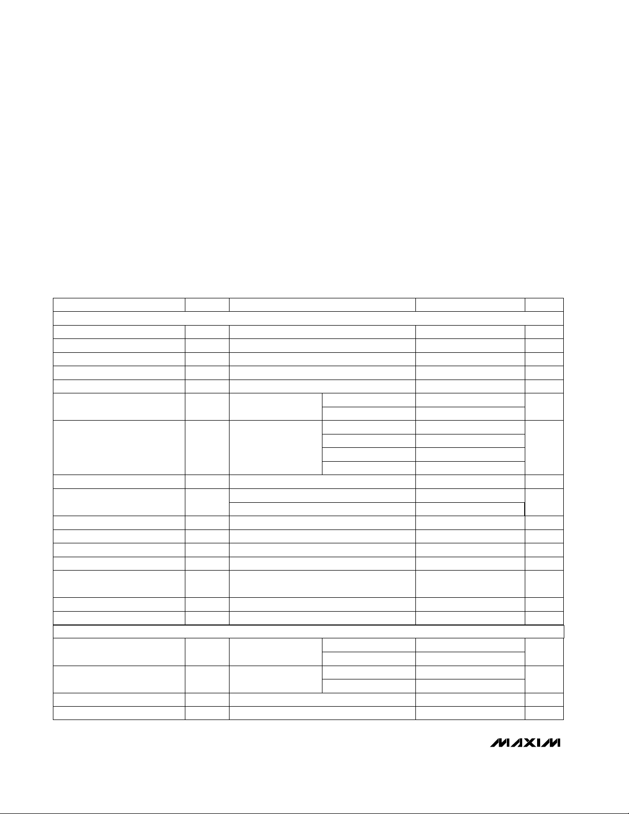
Typical Operating Circuit
19-1821; Rev 0; 11/00
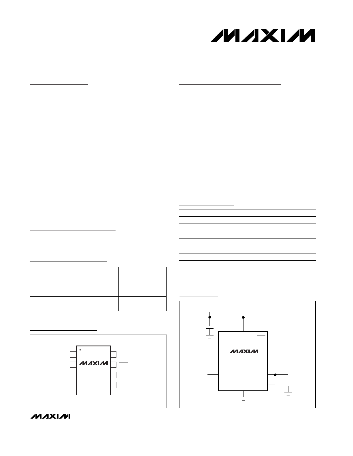
Pin Configuration
Ordering Information
Selector Guide
PART
MAX7418EUA -40°C to +85°C
TEMP. RANGE PIN-PACKAGE
8 µMAX
Selector Guide continued at end of data sheet.
Ordering Information continued at end of data sheet.
MAX7418CUA
0°C to +70°C 8 µMAX
MAX7419CUA
0°C to +70°C 8 µMAX
MAX7419EUA -40°C to +85°C 8 µMAX
MAX7420CUA
0°C to +70°C 8 µMAX
MAX7420EUA -40°C to +85°C 8 µMAX
MAX7421CUA
0°C to +70°C 8 µMAX
MAX7421EUA -40°C to +85°C 8 µMAX
PART FILTER RESPONSE
OPERATING
VOLTAGE (V)
MAX7418 r = 1.6 +5
MAX7419 Bessel +5
MAX7420 Butterworth +5
MAX7421 r = 1.25 +5
87CLK
SHDNIN
OS
6
OUTV
5
TOP VIEW
COM
GND
1
2
3
4
DD
MAX7418–
MAX7425
V
SUPPLY
0.1µF
V
DD
SHDN
INPUT
CLOCK
IN
MAX7418–
MAX7425
CLK
GND
OUT
COM
OUTPUT
OS
0.1µF
µMAX
Page 2
MAX7418–MAX7425
5th-Order, Lowpass,
Switched-Capacitor Filters
2 _______________________________________________________________________________________
ABSOLUTE MAXIMUM RATINGS
ELECTRICAL CHARACTERISTICS—MAX7418–MAX7421
(VDD= +5V, filter output measured at OUT, 10kΩ || 50pF load to GND at OUT, OS = COM, 0.1µF capacitor from COM to GND,
SHDN = V
DD
, f
CLK
= 2.2MHz, TA= T
MIN
to T
MAX
, unless otherwise noted. Typical values are at TA= +25°C.)
Stresses beyond those listed under “Absolute Maximum Ratings” may cause permanent damage to the device. These are stress ratings only, and functional
operation of the device at these or any other conditions beyond those indicated in the operational sections of the specifications is not implied. Exposure to
absolute maximum rating conditions for extended periods may affect device reliability.
VDDto GND..............................................................-0.3V to +6V
IN, OUT, COM, OS, CLK, SHDN ................-0.3V to (V
DD
+ 0.3V)
OUT Short-Circuit Duration.......................................................1s
Continuous Power Dissipation (T
A
= +70°C)
8-Pin µMAX (derate 4.1mW/°C above +70°C) .............330mW
Operating Temperature Ranges
MAX74 _ _C_A ...................................................0°C to +70°C
MAX74 _ _E_A ................................................-40°C to +85°C
Junction Temperature......................................................+150°C
Storage Temperature Range .............................-65°C to +160°C
Lead Temperature (soldering, 10s) .................................+300°C
CLOCK
FILTER CHARACTERISTICS
86 110 135
±50 ±75
MAX7419/MAX7420
MAX7418/MAX7421
MAX7419/MAX7420
MAX7418/MAX7421
-0.2 0 +0.2MAX7419/MAX7420
MAX7418/MAX7421
0.001 to 30VIN= 4Vp-p (Note 1)
Input Voltage Range at OS
2.0 2.5 3.0
COM Voltage Range
Maximum Capacitive Output
Load Drive
UNITS
kHz
ppm/°C
V
mV
dB
V/V
V
V
kΩ
mVp-p
kΩ
pF
µA
µA
kHz
µA
V
V
Clock Output Current
(Internal Oscillator Mode)
I
CLK
±40 ±60
Clock Input High V
IH
4.5
Clock Input Low V
IL
0.5
V
CLK
= 0 or 5V
PARAMETER SYMBOL MIN TYP MAX
DC Insertion Gain with
Output Offset Removed
0 0.2 0.4
Output Offset Voltage V
OFFSET
±4 ±25
Output Voltage Range 0.25 V
DD
-
0.25
Clock-to-Corner Tempco 10
Offset Voltage Gain A
OS
1
V
COM
Corner Frequency f
c
Clock-to-Corner Ratio f
CLK/fC
100:1
2.3 2.5 2.7
V
OS
V
COM
±0.1
Input Resistance at COM R
COM
100 140
Clock Feedthrough 5
Resistive Output Load Drive R
L
10 1
C
L
50 500
Input Leakage Current at COM ±0.1 ±10
Input Leakage Current at OS ±0.1 ±10
Internal Oscillator Frequency f
OSC
68 87 106
CONDITIONS
Output, COM unconnected
V
COM
= V
DD
/ 2
(Note 2)
VIN= V
COM
= V
DD
/ 2
Input, OS externally driven
OS to OUT
Input, COM externally driven
SHDN = GND, V
COM
= 0 to V
DD
VOS= 0 to V
DD
C
OSC
= 1000pF
(Note 3)
-78MAX7419
MAX7418 -76
-78MAX7421
MAX7420
dB
Total Harmonic Distortion
plus Noise
THD+N
-67
fIN= 2kHz,
VIN= 4Vp-p,
measurement
bandwidth = 80kHz
FILTER CHARACTERISTICS
CLOCK
Page 3
MAX7418–MAX7425
5th-Order, Lowpass,
Switched-Capacitor Filters
_______________________________________________________________________________________ 3
Corner-Frequency Range
0.001 to 45
5th-Order, Lowpass,
Switched-Capacitor Filters
ELECTRICAL CHARACTERISTICS—MAX7418–MAX7421 (continued)
(VDD= +5V, filter output measured at OUT, 10kΩ || 50pF load to GND at OUT, OS = COM, 0.1µF capacitor from COM to GND,
SHDN = V
DD
, f
CLK
= 2.2MHz, TA= T
MIN
to T
MAX
, unless otherwise noted. Typical values are at TA= +25°C.)
ELECTRICAL CHARACTERISTICS—MAX7422–MAX7425
(VDD= +3V, filter output measured at OUT pin, 10kΩ || 50pF load to GND at OUT, OS = COM, 0.1µF capacitor from COM to GND,
SHDN = V
DD
, f
CLK
= 2.2MHz, TA= T
MIN
to T
MAX
, unless otherwise noted. Typical values are at TA= +25°C.)
FILTER CHARACTERISTICS
0.001 to 45
MAX7423/MAX7424
MAX7422/MAX7425
-0.2 0 +0.2MAX7423/MAX7424
MAX7422/MAX7425
UNITS
kHz
ppm/°C
V
mV
dB
V/V
V
kΩ
mVp-p
kΩ
pF
µA
µA
PARAMETER SYMBOL MIN TYP MAX
DC Insertion Gain with Output
Offset Removed
0 0.2 0.4
Output Offset Voltage V
OFFSET
±4 ±25
Output Voltage Range 0.25 VDD- 0.25
Clock-to-Corner Tempco 10
Offset Voltage Gain A
OS
1
V
COM
f
C
Clock-to-Corner Ratio f
CLK/fC
100:1
Input Voltage Range at OS V
OS
V
COM
±0.1
Input Resistance at COM R
COM
100 140
Clock Feedthrough 3
Resistive Output Load Drive R
L
10 1
C
L
50 500
Input Leakage Current at COM ±0.1 ±10
Input Leakage Current at OS ±0.1 ±10
CONDITIONS
V
COM
= V
DD
/ 2
(Note 2)
VIN= V
COM
= V
DD
/ 2
Measured with respect to COM
OS to OUT
VIN= 2.5Vp-p
(Note 1)
SHDN = GND, V
COM
= 0 to V
DD
VOS= 0 to V
DD
Maximum Capacitive Load
at OUT
-81MAX7423
MAX7422 -80
-80MAX7425
MAX7424
dB
Total Harmonic Distortion plus
Noise
THD+N
-70
fIN= 2kHz,
VIN= 2.5Vp-p,
measurement
bandwidth = 80kHz
1.4 1.5 1.6Input, COM externally driven
VCOM Voltage Range
1.4 1.5 1.6Output, COM internally driven
FILTER CHARACTERISTICS
SHUTDOWN
POWER REQUIREMENTS
3.4 4.1MAX7419/MAX7420
MAX7418/MAX7421
µA±0.2 ±10
V
SHDN
= 0 to V
DD
SHDN Input Leakage Current
UNITS
V
mA
µA
dB
V
V
Supply Voltage V
DD
4.5 5.5
I
DD
Supply Current
2.9 3.6
Shutdown Current I
SHDN
0.2 1
Power-Supply Rejection Ratio PSRR 70
SHDN Input High
V
SDH
4.5
SHDN Input Low
V
SDL
0.5
Operating mode,
no load
SHDN = GND
IN = COM (Note 4)
PARAMETER SYMBOL MIN TYP MAXCONDITIONS
Page 4
MAX7418–MAX7425
5th-Order, Lowpass,
Switched-Capacitor Filters
4 _______________________________________________________________________________________
FILTER CHARACTERISTICS
(VDD= +5V for MAX7418–MAX7421, VDD= +3V for MAX7422–MAX7425 filter output measured at OUT, 10kΩ
|| 50pF load to GND at
OUT, SHDN = V
DD
, f
CLK
= 2.2MHz, TA = T
MIN
to T
MAX
, unless otherwise noted.)
ELECTRICAL CHARACTERISTICS—MAX7422–MAX7425 (continued)
(VDD= +3V, filter output measured at OUT pin, 10kΩ || 50pF load to GND at OUT, OS = COM, 0.1µF capacitor from COM to GND,
SHDN = V
DD
, f
CLK
= 2.2MHz, TA= T
MIN
to T
MAX
, unless otherwise noted. Typical values are at TA= +25°C.)
CONDITIONS MIN TYP MAXSYMBOLPARAMETER
Measured at DC
SHDN = GND
0.5V
SDL
SHDN Input Low
2.5V
SDH
SHDN Input High
70PSRRPower-Supply Rejection Ratio
0.2 1I
SHDN
Shutdown Current
2.6 3.4
2.7 3.6V
DD
Supply Voltage
V
V
dB
µA
V
UNITS
SHDN Input Leakage Current
V
SHDN
= 0 to V
DD
±0.2 ±10 µA
C
OSC
= 1000pF
(Note 3)
68 87 106
f
OSC
Internal Oscillator Frequency kHz
0.5V
IL
Clock Input Low V
2.5V
IH
Clock Input High V
68 87 106
I
CLK
Clock Output Current (Internal
Oscillator Mode)
kHz
MAX7422/MAX7425
MAX7423/MAX7424 86 110 135
MAX7422/MAX7425
MAX7423/MAX7424 86 110 135
Operating mode,
no load
3.0 3.8
Supply Current I
DD
mA
MAX7422/MAX7425
MAX7423/MAX7424
MIN TYP MAXCONDITIONSPARAMETER
-0.4 ±0.2 0.4fIN= 0.38f
C
UNITS
Insertion Gain with DC Gain
Error Removed (Note 4)
dB
fIN= 0.68f
C
-0.4 ±0.2 0.4
-0.4 ±0.2 0.4fIN= 0.87f
C
-36 -33fIN= 1.25f
C
fIN= 0.97f
C
-0.4 ±0.2 0.4
-0.7 ±0.2 0.2fIN= f
C
fIN= 1.43f
C
-37.2 -35
-1 -0.74fIN= 0.5f
C
fIN= 3.25f
C
-37.2 -35
Insertion Gain Relative to
DC Gain
dB
fIN= f
C
-3.6 -3.0 -2.4
fIN= 4f
C
-41.0 -35
-67 -60fIN= 7f
C
CLOCK
POWER REQUIREMENTS
ELLIPTIC, r = 1.2—MAX7421/MAX7425
BESSEL FILTERS—MAX7419/MAX7423
SHUTDOWN
Page 5
MAX7418–MAX7425
5th-Order, Lowpass,
Switched-Capacitor Filters
_______________________________________________________________________________________ 5
Note 1: The maximum fCis defined as the clock frequency f
CLK
= 100 x fCat which the peak S / (THD+N) drops to 68dB with a
sinusoidal input at 0.2f
C
. Maximum fC increases as VINsignal amplitude decreases.
Note 2: DC insertion gain is defined as ∆V
OUT
/ ∆VIN.
Note 3: MAX7418/MAX7421/MAX7422/MAX7425: f
OSC
(kHz) ≅ 87x103/ C
OSC
(pF).
MAX7419/MAX7420/MAX7423/MAX7424: f
OSC
(kHz) ≅ 110x103/ C
OSC
(pF).
Note 4: PSRR is the change in output voltage from a V
DD
of 4.5V and a VDDof 5.5V.
-70 -65fIN= 5f
C
-47.5 -43
-3.6 -3.0 -2.4fIN= f
C
fIN= 3f
C
-0.3 0
dB
fIN= 0.5f
C
PARAMETER MIN TYP MAX UNITSCONDITIONS
BUTTERWORTH FILTERS—MAX7420/MAX7424BUTTERWORTH FILTERS—MAX7420/MAX7424
FILTER CHARACTERISTICS
(VDD= +5V for MAX7418–MAX7421, VDD= +3V for MAX7422–MAX7425 filter output measured at OUT, 10kΩ
|| 50pF load to GND at
OUT, SHDN = V
DD
, f
CLK
= 2.2MHz, TA = T
MIN
to T
MAX
, unless otherwise noted.)
__________________________________________Typical Operating Characteristics
(VDD= +5V for MAX7418–MAX7421, VDD= +3V for MAX7422–MAX7425, f
CLK
= 2.2MHz, SHDN = VDD, V
COM
= VOS= VDD/ 2,
T
A
= +25°C, unless otherwise noted.)
-90
-60
-70
-80
-50
-40
-30
-20
-10
0
10
04020 60 80 100
MAX7418/MAX7422
FREQUENCY RESPONSE (ELLIPTIC, r = 1.6)
MAX7418 toc01
INPUT FREQUENCY (kHz)
GAIN (dB)
-60
-40
-50
-20
-30
0
-10
10
04020 60 80 100
MAX7419/MAX7423
FREQUENCY RESPONSE (BESSEL)
MAX7418 toc02
INPUT FREQUENCY (kHz)
GAIN (dB)
-80
-60
-70
-30
-40
-50
0
-10
-20
10
04020 60 80 100
MAX7420/MAX7424
FREQUENCY RESPONSE (BUTTERWORTH)
MAX7418 toc03
INPUT FREQUENCY (kHz)
GAIN (dB)
Insertion Gain Relative to
DC Gain
Page 6

____________________________Typical Operating Characteristics (continued)
(VDD= +5V for MAX7418–MAX7421, VDD= +3V for MAX7422–MAX7425, f
CLK
= 2.2MHz, SHDN = VDD, V
COM
= VOS= VDD/ 2,
T
A
= +25°C, unless otherwise noted.
MAX7418–MAX7425
5th-Order, Lowpass,
Switched-Capacitor Filters
6 _______________________________________________________________________________________
)
)
)
MAX7421/MAX7425
FREQUENCY RESPONSE (ELLIPTIC, r = 1.25)
10
0
-10
-20
-30
-40
GAIN (dB)
-50
-60
-70
-80
-90
04020 60 80 100
INPUT FREQUENCY (kHz)
MAX7418 toc04
0.4
0.2
-0.2
GAIN (dB)
-0.4
-0.6
-0.8
-1.0
MAX7420/MAX7424
PASSBAND FREQUENCY RESPONSE
0.5
0
-0.5
-1.0
-1.5
-2.0
GAIN (dB)
-2.5
-3.0
-3.5
-4.0
09.04.5 13.5 18.0 22.5
0
-50
-100
-150
PHASE SHIFT (DEGREES)
-200
-250
084 1216202428
(BUTTERWORTH)
INPUT FREQUENCY (kHz)
MAX7419/MAX7423
PHASE RESPONSE (BESSEL)
INPUT FREQUENCY (kHz
0.4
0.2
MAX7418 toc07
-0.2
GAIN (dB)
-0.4
-0.6
-0.8
-1.0
0
-50
MAX7418 toc10
-100
-150
-200
-250
PHASE SHIFT (DEGREES)
-300
-350
0
0 9.04.5 13.5 18.0 22.5
0
0 9.04.5 13.5 18.0 22.5
08124 16202428
MAX7418/MAX7422
PASSBAND FREQUENCY RESPONSE
(ELLIPTIC, r = 1.6)
INPUT FREQUENCY (kHz)
MAX7421/MAX7425
PASSBAND FREQUENCY RESPONSE
(ELLIPTIC, r = 1.25)
INPUT FREQUENCY (kHz)
MAX7420/MAX7424
PHASE RESPONSE (BUTTERWORTH)
INPUT FREQUENCY (kHz
0.5
MAX7418 toc05
MAX7418 toc08
MAX7418 toc11
0
-0.5
-1.0
-1.5
-2.0
GAIN (dB)
-2.5
-3.0
-3.5
-4.0
0
-50
-100
-150
-200
-250
-300
PHASE SHIFT (DEGREES)
-350
-400
-450
0
-50
-100
-150
-200
-250
-300
PHASE SHIFT (DEGREES)
-350
-400
-450
MAX7419/MAX7423
PASSBAND FREQUENCY RESPONSE
(BESSEL)
09.04.5 13.5 18.0 22.5
INPUT FREQUENCY (kHz)
MAX7418/MAX7422
PHASE RESPONSE (ELLIPTIC, r = 1.6)
08124 16202428
INPUT FREQUENCY (kHz)
MAX7424/MAX7425
PHASE RESPONSE (ELLIPTIC, r = 1.25)
08124 16202428
INPUT FREQUENCY (kHz
MAX7418 toc06
MAX7418 toc09
MAX7418 toc12
Page 7

____________________________Typical Operating Characteristics (continued)
(VDD= +5V for MAX7418–MAX7421, VDD= +3V for MAX7422–MAX7425, f
CLK
= 2.2MHz, SHDN = VDD, V
COM
= VOS= VDD/ 2,
T
A
= +25°C, unless otherwise noted.
MAX7418–MAX7425
5th-Order, Lowpass,
Switched-Capacitor Filters
_______________________________________________________________________________________ 7
MAX
8
THD
N
(dB)
E
MAX7424
MAX7425
THD + NOISE vs. INPUT SIGNAL AMPLITUDE
741
THD + NOISE vs. INPUT SIGNAL AMPLITUD
(ELLIPTIC, r = 1.6)
0
SEE TABLE A
-10
-20
-30
-40
+
-50
-60
-70
-80
-90
021 345
AMPLITUDE (Vp-p)
D
E
MAX7418 toc13
0
SEE TABLE A
-10
-20
-30
-40
-50
THD + N (dB)
-60
-70
-80
-90
021 345
MAX7421
THD + NOISE vs. INPUT SIGNAL AMPLITUDE
THD + NOISE vs. INPUT SIGNAL AMPLITUDE
(ELLIPTIC, r = 1.25)
0
SEE TABLE A
-10
-20
-30
-40
-50
THD + N (dB)
-60
-70
-80
-90
021 345
D
E
AMPLITUDE (Vp-p)
MAX7418 toc16
0
SEE TABLE A
-10
-20
-30
-40
-50
THD + N (dB)
-60
-70
-80
-90
0 1.00.5 1.5 2.0 2.5 3.0
MAX7419
(BESSEL)
D
E
AMPLITUDE (Vp-p)
MAX7422
(ELLIPTIC, r = 1.6)
C
AMPLITUDE (Vp-p)
MAX7418 toc14
MAX7418 toc17
A
B
MAX7420
THD + NOISE vs. INPUT SIGNAL AMPLITUDE
(BUTTERWORTH)
0
SEE TABLE A
-10
-20
-30
-40
-50
THD + N (dB)
-60
-70
-80
-90
021 345
D
E
AMPLITUDE (Vp-p)
MAX7423
THD + NOISE vs. INPUT SIGNAL AMPLITUDE
(BESSEL)
0
SEE TABLE A
-10
-20
-30
-40
-50
THD + N (dB)
-60
-70
-80
-90
01.00.5 1.5 2.0 2.5 3.0
A
B
C
AMPLITUDE (Vp-p)
MAX7418 toc15
MAX7418 toc18
THD + NOISE vs. INPUT SIGNAL AMPLITUDE
(BUTTERWORTH)
0
SEE TABLE A
-10
-20
-30
-40
-50
THD + N (dB)
-60
-70
-80
-90
C
0 0.5 1.0 1.5 2.0 2.5 3.0
AMPLITUDE (Vp-p)
B
A
MAX7418 toc19
THD + NOISE vs. INPUT SIGNAL AMPLITUDE
(ELLIPTIC, r = 1.25)
0
SEE TABLE A
-10
-20
-30
-40
-50
THD + N (dB)
-60
-70
-80
-90
0 0.5 1.0 1.5 2.0 2.5 3.0
A
B
C
AMPLITUDE (Vp-p)
INTERNAL OSCILLATOR FREQUENCY
vs. SMALL CAPACITANCE (pF)
7000
6000
MAX7418 toc20
5000
4000
3000
ELLIPTIC
2000
OSCILLATOR FREQUENCY (kHz)
1000
0
1 10 100 1000 10000
MAX7418 toc21
BESSEL/BUTTERWORTH
CAPACITANCE ( pF)
Page 8

____________________________Typical Operating Characteristics (continued)
(VDD= +5V for MAX7418–MAX7421, VDD= +3V for MAX7422–MAX7425, f
CLK
= 2.2MHz, SHDN = VDD, V
COM
= VOS= VDD/ 2,
T
A
= +25°C, unless otherwise noted.
MAX7418–MAX7425
5th-Order, Lowpass,
Switched-Capacitor Filters
8 _______________________________________________________________________________________
1
f
IN
(kHz)
2
2
1
2
10
f
C
(kHz)
E
30
22
10
22
1000
LABEL
A
B
f
CLK
(kHz)
3000
2200
1000C
D 2200
22
BW
(kHz)
80
80
22
80
Table A.
INTERNAL OSCILLATOR FREQUENCY
vs. LARGE CAPACITANCE (nF)
6
ELLIPTIC INTERNAL OSCILLATOR
FREQUENCY vs. SUPPLY VOLTAGE
87.0
5
4
3
2
ELLIPTIC
OSCILLATOR FREQUENCY (Hz)
1
0
10 100 1000
BESSEL/BUTTERWORTH
CAPACITANCE (nF)
ELLIPTIC INTERNAL OSCILLATOR
FREQUENCY vs. TEMPERATURE
87.0
86.5
86.0
85.5
85.0
OSCILLATOR FREQUENCY (kHz)
84.5
C
= 1000pF
OSC
84.0
-40 10-15 356085
ELLIPTIC SUPPLY CURRENT
3.0
VDD = 3V
VDD = 5V
TEMPERATURE (°C)
vs. TEMPERATURE
MAX7418 toc22
MAX7418 toc24
86.5
86.0
85.5
85.0
OSCILLATOR FREQUENCY (kHz)
84.5
C
= 1000PF
OSC
84.0
2.5 3.5 4.03.0 4.5 5.0 5.5
SUPPLY VOLTAGE (V)
ELLIPTIC SUPPLY CURRENT
vs. SUPPLY VOLTAGE
3.3
3.1
2.9
2.7
SUPPLY CURRENT (µA)
2.5
2.3
2.5 3.53.0 4.0 4.5 5.0 5.5
SUPPLY VOLTAGE (V)
MAX7418 toc23
MAX7418 toc25
2.9
2.8
2.7
SUPPLY CURRENT (mA)
2.6
2.5
-40 10-15 35 60 85
VDD = 5V
VDD = 3V
TEMPERATURE (°C)
MAX7418 toc26
Page 9

MAX7418–MAX7425
5th-Order, Lowpass,
Switched-Capacitor Filters
_______________________________________________________________________________________ 9
Pin Description
_______________Detailed Description
The MAX7418/MAX7421/MAX7422/MAX7425 elliptic
lowpass filters provide sharp rolloff with good stopband
rejection. The MAX7419/MAX7423 Bessel filters provide
low overshoot and fast settling responses, and the
MAX7420/MAX7424 Butterworth filters provide a maximally flat passband response. All parts operate with a
100:1 clock-to-corner frequency ratio.
Most switch capacitor filters (SCFs) are designed with
biquadratic sections. Each section implements two
pole-zero pairs, and the sections can be cascaded to
produce higher order filters. The advantage to this
approach is ease of design. However, this type of
design is highly sensitive to component variations if any
section’s Q is high. The MAX7418–MAX7425 use an
alternative approach, which is to emulate a passive network using switched-capacitor integrators with summing and scaling. The passive network may be
synthesized using CAD programs, or may be found in
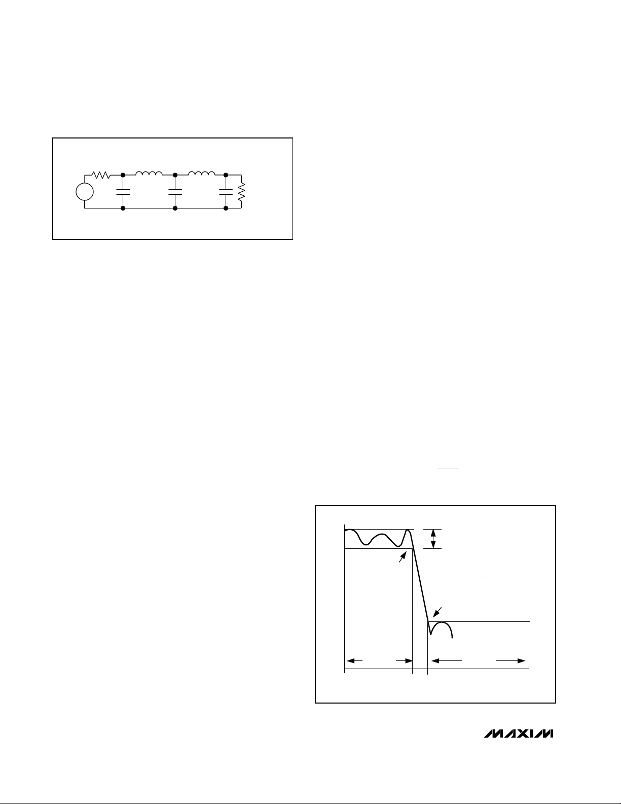
many filter books. Figure 1 shows a basic 5th-order ladder filter structure.
Typical Operating Characteristics (continued)
(VDD= +5V for MAX7418–MAX7421, VDD= +3V for MAX7422–MAX7425, f
CLK
= 2.2MHz, SHDN = VDD, V
COM
= VOS= VDD/ 2,
T
A
= +25°C, unless otherwise noted.
0
0.5
1.5
1.0
2.0
2.5
2.5 3.53.0 4.0 4.5 5.0 5.5
DC OFFSET VOLTAGE
vs. SUPPLY VOLTAGE
MAX7418 toc28
SUPPLY VOLTAGE (V)
DC OFFSET VOLTAGE (mV)
0
1.0
0.5
2.0
1.5
2.5
3.0
-40 10-15 356085
DC OFFSET VOLTAGE
vs. TEMPERATURE
MAX7418 toc27
TEMPERATURE (°C)
DC OFFSET VOLTAGE (mV)
VDD = 5V
VDD = 3V
Filter OutputOUT5
Offset Adjust Input. To adjust output offset, connect OS to an external supply through a resistive voltagedivider (Figure 4). Connect OS to COM if no offset adjustment is needed. See the Offset and Common-Mode
Input Adjustment section.
OS6
Shutdown Input. Drive low to enable shutdown mode; drive high or connect to VDDfor normal operation.
SHDN
7
Clock Input. Connect an external capacitor (C
OSC
) from CLK to ground. To override the internal oscillator,
connect CLK to an external clock: f
C
= f
CLK
/100.
CLK8
Positive Supply Input: +5V for MAX7418–MAX7421, +3V for MAX7422–MAX7425. Bypass V
DD
to GND with
a 0.1µF capacitor.
V
DD
4
Ground GND3
PIN
Filter InputIN2
Common Input Pin. Biased internally at midsupply. Bypass COM externally to GND with a 0.1µF capacitor.
To override internal biasing, drive COM with an external supply.
COM1
FUNCTIONNAME
Page 10
MAX7418–MAX7425
5th-Order, Lowpass,
Switched-Capacitor Filters
10 ______________________________________________________________________________________
An SCF that emulates a passive ladder filter retains
many of the same advantages. The component sensitivity of a passive ladder filter is low when compared to
a cascaded biquadratic design because each component affects the entire filter shape rather than a single
pole-zero pair. In other words, a mismatched component in a biquadratic design has a concentrated error
on its respective poles, while the same mismatch in a
ladder filter design spreads its error over all poles.
Elliptic Characteristics
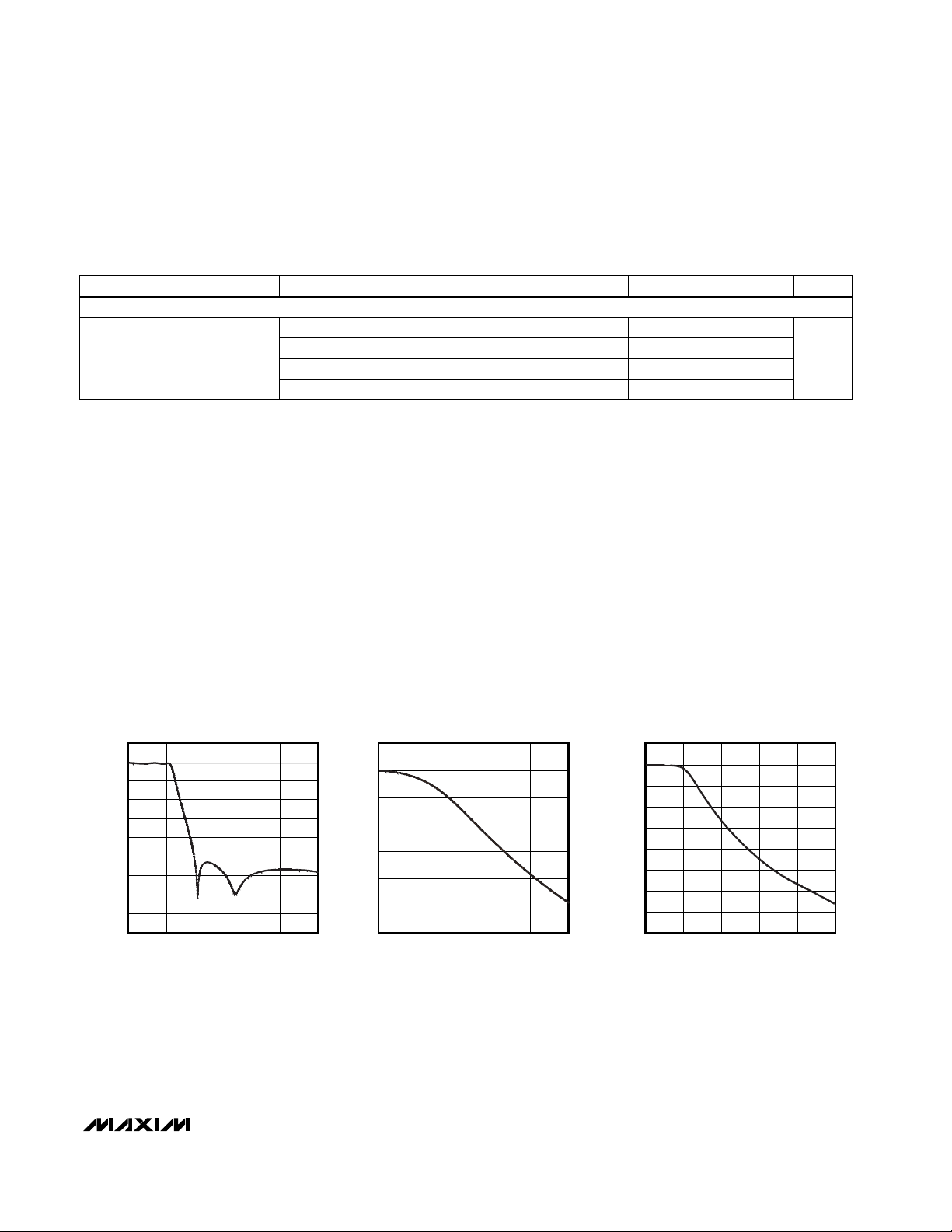
Lowpass elliptic filters such as the MAX7418/MAX7421/
MAX7422/MAX7425 provide the steepest possible
rolloff with frequency of the four most common filter
types (Butterworth, Bessel, Chebyshev, and elliptic).
The high-Q value of the poles near the passband edge
combined with the stopband zeros allow for the sharp
attenuation characteristic of elliptic filters, making these
devices ideal for anti-aliasing and post-DAC filtering in
single-supply systems (see Anti-Aliasing and Post-DAC
Filtering).
In the frequency domain, the first transmission zero
causes the filter’s amplitude to drop to a minimum level
(Figure 2). Beyond this zero, the response rises as the
frequency increases until the next transmission zero.
The stopband begins at the stopband frequency, f
S
. At
frequencies above f
S
, the filter’s gain does not exceed
the gain at f
S
. The corner frequency, fC, is defined as
the point at which the filter output attenuation falls just
below the passband ripple. The transition ratio (r) is
defined as the ratio of the stopband frequency to the
corner frequency:
r = f
S
/ f
C
The MAX7418/MAX7422 have a transition ratio of 1.6
and typically 53dB of stopband rejection. The
MAX7421/MAX7425 have a transition ratio of 1.25 (providing a steeper rolloff) and typically 37dB of stopband
rejection.
Bessel Characteristics
Lowpass Bessel filters such as the MAX7419/MAX7423
delay all frequency components equally, preserving the
line up shape of step inputs (subject to the attenuation
of the higher frequencies). Bessel filters settle quickly—
an important characteristic in applications that use a
multiplexer (mux) to select an input signal for an analog-to-digital converter (ADC). An anti-aliasing filter
placed between the mux and the ADC must settle
quickly after a new channel is selected.
Butterworth Characteristics
Lowpass Butterworth filters such as the MAX7420/
MAX7424 provide a maximally flat passband response,
making them ideal for instrumentation applications that
require minimum deviation from the DC gain throughout
the passband.
The difference between Bessel and Butterworth filters
can be observed when a 1kHz square wave is applied
to the filter input (Figure 3, trace A). With the filter cutoff
frequencies set at 5kHz, trace B shows the Bessel filter
response and trace C shows the Butterworth filter
response.
Clock Signal
External Clock
These SCFs are designed for use with external clocks
that have a 40% to 60% duty cycle. When using an
external clock, drive the CLK pin with a CMOS gate
powered from 0 to V
DD
. Varying the rate of the external
clock adjusts the corner frequency of the filter:
Figure 1. 5th-Order Ladder Filter Network
Figure 2. Elliptic Filter Response
R
S
+
V
IN
-
L2
C1
L4
C5C3
R
L
GAIN (dB)
PASSBAND STOPBAND
f
f
f
C
CLK
=
C
100
RIPPLE
TRANSITION RATIO =
f
S
f
CfS
f
S
f
C
FREQUENCY
Page 11

MAX7418–MAX7425
5th-Order, Lowpass,
Switched-Capacitor Filters
______________________________________________________________________________________ 11
Internal Clock
When using the internal oscillator, the capacitance
(C
OSC
) on CLK determines the oscillator frequency:
where
k = 87 x 103 for the
MAX7418/MAX7421/MAX7422/MAX7425
and
k = 110 x 103for the
MAX7419/MAX7420/MAX7423/ MAX7424.
Since C
OSC
is in the low picofarads, minimize the stray
capacitance at CLK so that it does not affect the internal oscillator frequency. Varying the rate of the internal
oscillator adjusts the filter’s corner frequency by a
100:1 clock-to-corner frequency ratio. For example, an
internal oscillator frequency of 2.2MHz produces a
nominal corner frequency of 2.2kHz.
Input Impedance vs. Clock Frequencies
The MAX7418–MAX7425s’ input impedance is effective
as a switched-capacitor resistor and is inversely proportional to frequency. The input impedance values determined by the equation represents the average input
impedance, since the input current is not continuous.
As a rule, use a driver with an output resistance less
than 10% of the filter’s input impedance.
Estimate the input impedance of the filter by using the
following formula:
where f
CLK
= clock frequency and CIN= 1pF.
Low-Power Shutdown Mode
The MAX7418–MAX7425 have a shutdown mode that is
activated by driving SHDN low. In shutdown mode, the
filter supply current reduces to 0.2µA, and the output of
the filter becomes high impedance. For normal operation, drive SHDN high or connect to VDD.
Applications Information
Offset (OS) and Common-Mode (COM)
Input Adjustment
COM sets the common-mode input voltage and is
biased at midsupply with an internal resistor-divider. If
the application does not require offset adjustment, connect OS to COM. For applications in which offset
adjustment is required, apply an external bias voltage
through a resistor-divider network to OS, as shown in
Figure 4. For applications that require DC level shifting,
adjust OS with respect to COM. (Note: Do not leave OS
unconnected.) The output voltage is represented by
these equations:
where (VIN- V
COM
) is lowpass filtered by the SCF and
OS is added at the output stage. See the Electrical
Characteristics table for the input voltage range of COM
Figure 4. Offset Adjustment Circuit
Figure 3. Bessel vs. Butterworth Filter Response
2V/div
A
2V/div
B
2V/div
C
200µs/div
A: 1kHz INPUT SIGNAL
B: MAX7419 BESSEL FILTER RESPONSE; f
C: MAX7420 BUTTERWORTH FILTER RESPONSE; f
= 5kHz
C
= 5kHz
C
f
OSC
(kHz)
=
C
OSC
k
(pF)
V
SUPPLY
0.1µF
V
DD
INPUT
CLOCK
IN
MAX7418–
MAX7425
CLK
GND
Z
=
IN
(f C )
CLK IN
SHDN
OUT
COM
OS
1
×
0.1µF
0.1µF
OUTPUT
50k
50k
50k
VVVV
( )
=− +
OUT IN COM OS
V
V
COM
DD
()
=
typ
2
Page 12

MAX7418–MAX7425
5th-Order, Lowpass,
Switched-Capacitor Filters
12 ______________________________________________________________________________________
and OS. Changing the voltage on COM or OS significantly from midsupply reduces the dynamic range.
Power Supplies
The MAX7418–MAX7421 operate from a single +5V
supply and the MAX7422–MAX7425 operate from a single +3V supply. Bypass VDDto GND with a 0.1µF
capacitor. If dual supplies are required, connect COM
to the system ground and GND to the negative supply.
Figure 5 shows an example of dual-supply operation.
Single-supply and dual-supply performance are equivalent. For either single-supply or dual-supply operation,
drive CLK and SHDN from GND (V- in dual supply
operation) to V
DD
. Use the MAX7418–MAX7421 for
±2.5, and use the MAX7422–MAX7425 for ±1.5V. For
±5V dual-supply applications, refer to the MAX291/
MAX292/MAX295/MAX296 and MAX293/MAX294/
MAX297 data sheets.
Input Signal Amplitude Range
The optimal input signal range is determined by observing the voltage level at which the signal-to-noise plus
distortion (SINAD) ratio is maximized for a given corner
frequency. The Typical Operating Characteristics show
the THD + Noise response as the input signal’s peak-topeak amplitude is varied.
Anti-Aliasing and Post-DAC Filtering
When using the MAX7418–MAX7425 for anti-aliasing or
post-DAC filtering, synchronize the DAC (or ADC) and
the filter clocks. If the clocks are not synchronized, beat
frequencies may alias into the desired passband.
Harmonic Distortion
Harmonic distortion arises from nonlinearities within the
filter. These nonlinearities generate harmonics when a
pure sine wave is applied to the filter input. Tables 1, 2,
and 3 list typical harmonic distortion values with a 10kΩ
load at TA= +25°C.
Table 1. MAX7418/MAX7421/MAX7422/MAX7425 Typical Harmonic Distortion
FILTER
f
IN
(kHz)
V
IN
(Vp-p)
MAX7418
2
MAX7421
2
2
4
2nd 4th
f
CLK
(MHz)
2.2
1.5
2
<-80<-80
<-80
MAX7422
4
TYPICAL HARMONIC DISTORTION (dB)
<-80
<-80
4
2
2
4.0
2.2
<-80<-80
<-80
<-80
<-80
<-80
<-80
<-80
<-80
<-80 <-80
3rd 5th
2.2
1.5
<-80<-80
<-80
4
<-80
<-80
MAX7425
2
2
4.0
2.2
<-80
<-80
<-80
<-80
<-80
<-80
<-80
<-80
<-80
<-80
<-80
Figure 5. Dual-Supply Operation
V+
SHDN
COM
*
OUTPUTOUT
OS
0.1µF
0.1µF
V
DD
IN
INPUT
MAX7418–
V+
V-
*CONNECT SHDN TO V- FOR LOW-POWER SHUTDOWN MODE.
CLOCK
MAX7425
CLK
GND
V-
Page 13

MAX7418–MAX7425
5th-Order, Lowpass,
Switched-Capacitor Filters
______________________________________________________________________________________ 13
Table 3. MAX7419/MAX7423 Typical Harmonic Distortion
Table 2. MAX7420/MAX7424 Typical Harmonic Distortion
Chip Information
TRANSISTOR COUNT: 1457
PROCESS: BiCMOS
Ordering Information (continued)
PART TEMP. RANGE PIN-PACKAGE
MAX7423CUA
MAX7423EUA -40°C to +85°C
0°C to +70°C 8 µMAX
8 µMAX
MAX7422CUA
0°C to +70°C 8 µMAX
MAX7422EUA -40°C to +85°C 8 µMAX
PART
FILTER RESPONSE
OPERATING
VOLTAGE (V)
MAX7422 r = 1.6 +3
MAX7423 Bessel +3
MAX7424 Butterworth +3
MAX7425 r = 1.25 +3
Selector Guide (continued)
MAX7424CUA
0°C to +70°C 8 µMAX
MAX7424EUA -40°C to +85°C 8 µMAX
MAX7425CUA
0°C to +70°C 8 µMAX
MAX7425EUA -40°C to +85°C 8 µMAX
FILTER
f
IN
(kHz)
V
IN
(Vp-p)
MAX7420
2
2
4
-77
< -80
TYPICAL HARMONIC DISTORTION (dB)
< -80
< -80
2nd
4th
f
CLK
(MHz)
2.2
1.5
3
MAX7424
2
2
3.5
2.2
< -80
< -80
< -80
< -80
-67 -76
-70
-70
-77
< -80
< -80
< -80
3rd 5th
FILTER
f
IN
(kHz)
V
IN
(Vp-p)
MAX7419
2
2
4
< -80
< -80
TYPICAL HARMONIC DISTORTION (dB)
< -80
< -80
2nd
4th
f
CLK
(MHz)
2.2
1.5
3
MAX7423
2
2
3.5
2.2
< -80
< -80
< -80
< -80
-77 < -80
-80
-75
< -80
< -80
< -80
< -80
3rd 5th
Page 14
MAX7418–MAX7425
5th-Order, Lowpass,
Switched-Capacitor Filters
Maxim cannot assume responsibility for use of any circuitry other than circuitry entirely embodied in a Maxim product. No circuit patent licenses are
implied. Maxim reserves the right to change the circuitry and specifications without notice at any time.
14 ____________________Maxim Integrated Products, 120 San Gabriel Drive, Sunnyvale, CA 94086 408-737-7600
© 2000 Maxim Integrated Products Printed USA is a registered trademark of Maxim Integrated Products.
________________________________________________________Package Information
8LUMAXD.EPS
 Loading...