

Page 1
General Description
The MAX7400/MAX7403/MAX7404/MAX7407 8th-order,
lowpass, elliptic, switched-capacitor filters (SCFs) operate from a single +5V (MAX7400/MAX7403) or +3V
(MAX7404/MAX7407) supply. These devices draw 2mA
of supply current and allow corner frequencies from
1Hz to 10kHz, making them ideal for low-power antialiasing and post-DAC filtering applications. They feature a shutdown mode that reduces the supply current
to 0.2µA.
Two clocking options are available: self-clocking
(through the use of an external capacitor) or external
clocking for tighter cutoff-frequency control. In addition,
an offset adjustment pin (OS) allows for the adjustment
of the DC output level.
The MAX7400/MAX7404 provide 82dB of stopband
rejection and a sharp rolloff with a transition ratio of 1.5.
The MAX7403/MAX7407 provide a sharper rolloff with a
transition ratio of 1.2, while still delivering 60dB of stopband rejection. The fixed response of these devices
simplifies the design task to corner-frequency selection
by setting a clock frequency. The MAX7400/
MAX7403/MAX7404/MAX7407 are available in 8-pin SO
and DIP packages.
Applications
ADC Anti-Aliasing Speech Processing
Post-DAC Filtering Air-Bag Electronics
CT2 Base Stations
Features
♦ 8th-Order Lowpass Elliptic Filter
♦ Low Noise and Distortion
-82dB THD + Noise (MAX7400)
♦ Clock-Tunable Corner Frequency (1Hz to 10kHz)
♦ 100:1 Clock-to-Corner Ratio
♦ Single-Supply Operation
+5V (MAX7400/MAX7403)
+3V (MAX7404/MAX7407)
♦ Low Power
2mA (Operating Mode)
0.2µA (Shutdown Mode)
♦ Available in 8-Pin SO and DIP Packages
♦ Low Output Offset: ±5mV
MAX7400/MAX7403/MAX7404/MAX7407
8th-Order, Lowpass, Elliptic,
Switched-Capacitor Filters
________________________________________________________________
Maxim Integrated Products
1
V
DD
IN
CLK
OUT
GND
INPUT
0.1µF
0.1µF
CLOCK
SHDN
OUTPUT
V
SUPPLY
COM
OS
MAX7400
MAX7403
MAX7404
MAX7407
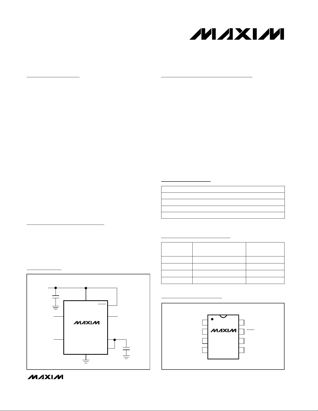
Typical Operating Circuit
19-4764; Rev 2; 6/99
Ordering Information continued at end of data sheet.
Pin Configuration
Ordering Information
Selector Guide
MAX7407 Elliptic (r = 1.2) +3
PART FILTER RESPONSE
OPERATING
VOLTAGE (V)
MAX7403
MAX7400 Elliptic (r = 1.5) +5
Elliptic (r = 1.2) +5
MAX7404 Elliptic (r = 1.5) +3
PART
MAX7400CSA
MAX7400CPA
MAX7400ESA -40°C to +85°C
0°C to +70°C
0°C to +70°C
TEMP. RANGE PIN-PACKAGE
8 SO
8 Plastic DIP
8 SO
MAX7400EPA -40°C to +85°C 8 Plastic DIP
For free samples & the latest literature: http://www.maxim-ic.com, or phone 1-800-998-8800.
For small orders, phone 1-800-835-8769.
TOP VIEW
COM
1
GND
2
MAX7400
MAX7403
3
MAX7404
MAX7407
4
DD
SO/DIP
87CLK
SHDNIN
OS
6
OUTV
5
Page 2
MAX7400/MAX7403/MAX7404/MAX7407
8th-Order, Lowpass, Elliptic,
Switched-Capacitor Filters
2 _______________________________________________________________________________________
ABSOLUTE MAXIMUM RATINGS
ELECTRICAL CHARACTERISTICS—MAX7400/MAX7403
(VDD= +5V, filter output measured at OUT, 10kΩ || 50pF load to GND at OUT, SHDN = VDD, OS = COM, 0.1µF from COM to GND,
f
CLK
= 100kHz, TA= T
MIN
to T
MAX
, unless otherwise noted. Typical values are at +25°C.)
Stresses beyond those listed under “Absolute Maximum Ratings” may cause permanent damage to the device. These are stress ratings only, and functional
operation of the device at these or any other conditions beyond those indicated in the operational sections of the specifications is not implied. Exposure to
absolute maximum rating conditions for extended periods may affect device reliability.
VDDto GND
MAX7400/MAX7403 ..............................................-0.3V to +6V
MAX7404/MAX7407 ..............................................-0.3V to +4V
IN, OUT, COM, OS, CLK............................-0.3V to (V
DD
+ 0.3V)
SHDN........................................................................-0.3V to +6V
OUT Short-Circuit Duration...................................................1sec
Continuous Power Dissipation (T
A
= +70°C)
SO (derate 5.88mW/°C above +70°C)..........................471mW
DIP (derate 9.1mW/°C above +70°C)...........................727mW
Operating Temperature Ranges
MAX740_C_A .....................................................0°C to +70°C
MAX740_E_A ..................................................-40°C to +85°C
Storage Temperature Range.............................-65°C to +150°C
Lead Temperature (soldering, 10sec).............................+300°C
VOS= 0 to (VDD- 1V) (Note 3)
(Note 1)
SHDN = GND, V
COM
= 0 to V
DD
VIN= V
COM
= VDD/ 2
Output, COM internally biased
V
COM
= VDD/ 2 (Note 2)
Input, COM externally driven
CONDITIONS
µA±0.1 ±10Input Leakage Current at OS
µA±0.1 ±10Input Leakage Current at COM
pF50 500C
L
Maximum Capacitive Load
at OUT
kΩ10 1R
L
Resistive Output Load Drive
mVp-p10Clock Feedthrough
kΩ75 125R
COM
Input Resistance at COM
VDD/ 2
V
DD
/ 2
V
DD
/ 2
- 0.2 + 0.2
V
COM
COM Voltage Range V
VDD/ 2
V
DD
/ 2
V
DD
/ 2
- 0.5 + 0.5
100:1f
CLK/fC
Clock-to-Corner Ratio
kHz0.001 to 10f
C
Corner Frequency
VV
COM
±0.1V
OS
Input Voltage Range at OS
-82
ppm/°C10Clock-to-Corner Tempco
V0.25 VDD- 0.25Output Voltage Range
mV±5 ±25V
OFFSET
Output Offset Voltage
dB-0.1 0.15 0.3
DC Insertion Gain with
Output Offset Removed
UNITSMIN TYP MAXSYMBOLPARAMETER
C
OSC
= 1000pF (Note 4) kHz29 38 48f
OSC
Internal Oscillator Frequency
V
CLK
= 0 or 5V µA±15 ±30I
CLK
Clock Input Current
VDD- 0.5V
IH
V
0.5V
IL
Clock Input High
fIN= 200Hz, VIN= 4Vp-p,
measurement bandwidth = 22kHz
dB
-80
THD+N
Total Harmonic Distortion
plus Noise
MAX7400
MAX7403
V/V1A
OS
OS Voltage Gain to OUT
Clock Input Low V
FILTER CHARACTERISTICS
CLOCK
Page 3
MAX7400/MAX7403/MAX7404/MAX7407
8th-Order, Lowpass, Elliptic,
Switched-Capacitor Filters
_______________________________________________________________________________________ 3
ELECTRICAL CHARACTERISTICS—MAX7400/MAX7403 (continued)
(VDD= +5V, filter output measured at OUT, 10kΩ || 50pF load to GND at OUT, SHDN = VDD, OS = COM, 0.1µF from COM to GND,
f
CLK
= 100kHz, TA= T
MIN
to T
MAX
, unless otherwise noted. Typical values are at TA= +25°C.)
ELECTRICAL CHARACTERISTICS—MAX7404/MAX7407
(VDD= +3V, filter output measured at OUT, 10kΩ || 50pF load to GND at OUT, SHDN = VDD, OS = COM, 0.1µF from COM to GND,
f
CLK
= 100kHz, TA= T
MIN
to T
MAX
, unless otherwise noted. Typical values are at TA= +25°C.)
SHUTDOWN
POWER REQUIREMENTS
SHDN Input Leakage Current
±0.1 ±10 µAV
SHDN
= 0 to V
DD
SHDN Input High
V
SDL
0.5
VV
SDH
VDD- 0.5
PARAMETER SYMBOL MIN TYP MAX UNITS
Power-Supply Rejection Ratio PSRR 60 dB
Shutdown Current I
SHDN
0.2 1 µA
Supply Voltage V
DD
4.5 5.5 V
Supply Current I
DD
2 3.5 mA
CONDITIONS
Measured at DC
SHDN = GND, CLK driven from 0 to V
DD
Operating mode, no load, IN = OS = COM
FILTER CHARACTERISTICS
Total Harmonic Distortion
plus Noise
PARAMETER SYMBOL MIN TYP MAX UNITS
DC Insertion Gain with Output
Offset Removed
-0.1 0.1 0.3 dB
Output Offset Voltage V
OFFSET
±5 ±25 mV
Output Voltage Range 0.25 VDD- 0.25 V
Clock-to-Corner Tempco 10 ppm/°C
THD+N
-77
dB
MAX7407
MAX7404 -79
OS Voltage Gain to OUT A
OS
1 V/V
Input Voltage Range at OS V
OS
V
COM
±0.1 V
Corner Frequency f
C
0.001 to 10 kHz
Clock-to-Corner Ratio f
CLK/fC
100:1
VDD/ 2
V
DD
/ 2
V
DD
/ 2
- 0.1 + 0.1
VCOM Voltage Range V
COM
Input Resistance at COM R
COM
75 125 kΩ
Clock Feedthrough 10 mVp-p
Resistive Output Load Drive R
L
10 1 kΩ
Maximum Capacitive Load
at OUT
C
L
50 500 pF
Input Leakage Current at COM ±0.1 ±10 µA
Input Leakage Current at OS ±0.1 ±10 µA
CONDITIONS
COM internally biased or externally driven
V
COM
= VDD/ 2 (Note 2)
VIN= V
COM
= VDD/ 2
fIN= 200Hz, VIN= 2.5Vp-p,
measurement bandwidth = 22kHz
SHDN = GND, V
COM
= 0 to V
DD
(Note 1)
VOS= 0 to (VDD- 1V) (Note 3)
SHDN Input Low
V
Page 4
MAX7400/MAX7403/MAX7404/MAX7407
8th-Order, Lowpass, Elliptic,
Switched-Capacitor Filters
4 _______________________________________________________________________________________
ELECTRICAL CHARACTERISTICS—MAX7404/MAX7407 (continued)
(VDD= +3V, filter output measured at OUT, 10kΩ || 50pF load to GND at OUT, SHDN = VDD, OS = COM, 0.1µF from COM to GND,
f
CLK
= 100kHz, TA= T
MIN
to T
MAX
, unless otherwise noted. Typical values are at TA= +25°C.)
ELLIPTIC (r = 1.5) FILTER CHARACTERISTICS—MAX7400/MAX7404
(VDD= +5V for MAX7400, VDD= +3V for MAX7404; filter output measured at OUT; 10kΩ || 50pF load to GND at OUT; SHDN = VDD;
V
COM
= VOS= V
DD
/ 2; f
CLK
= 100kHz; TA= T
MIN
to T
MAX
; unless otherwise noted. Typical values are at TA= +25°C.)
V
CLK
= 0 or 3V
C
OSC
= 1000pF (Note 4)
V
CONDITIONS
VDD- 0.5V
IH
µA±15 ±30I
CLK
Clock Input Current
kHz26 34 43f
OSC
Internal Oscillator Frequency
0.5V
IL
Clock Input High
UNITSMIN TYP MAXSYMBOLPARAMETER
SHDN = GND, CLK driven from 0 to V
DD
Operating mode, no load, IN = OS = COM
Measured at DC
µA0.2 1I
SHDN
mA2 3.5I
DD
Supply Current
V2.7 3.6V
DD
Supply Voltage
60PSRR
Shutdown Current
Power-Supply Rejection Ratio dB
VDD- 0.5V
SDH
SHDN Input High
V
V
SHDN
= 0 to V
DD
±0.1 ±10
SHDN Input Leakage Current
µA
V
SDL
0.5
Clock Input Low
SHDN Input Low
V
V
CLOCK
POWER REQUIREMENTS
SHUTDOWN
dB
CONDITIONS UNITSMIN TYP MAXPARAMETER
fIN= 0.371f
C
-0.20 -0.10 0.20
fIN= 0.737f
C
fIN= 0.587f
C
-0.20 -0.08 0.20
-0.20 0.02 0.20
fIN= 0.940f
C
fIN= 0.868f
C
-0.20 -0.03 0.20
fIN= 1.000f
C
fIN= 0.988f
C
-0.20 0.02 0.25
-0.20 0.09 0.25
-0.20 0.06 0.20
fIN= 1.601f
C
fIN= 1.500f
C
-84 -78
fIN= 4.020f
C
fIN= 2.020f
C
-85 -78
Insertion Gain Relative to DC Gain
(Note 5)
-83 -78
-82 -75
Page 5
8th-Order, Lowpass, Elliptic,
Switched-Capacitor Filters
_______________________________________________________________________________________ 5
Note 1: The maximum fCis defined as the clock frequency, f
CLK
= 100 · fC, at which the peak SINAD drops to 68dB with a
sinusoidal input at 0.2f
C
.
Note 2: DC insertion gain is defined as ∆V
OUT
/ ∆VIN.
Note 3: OS voltages above V
DD
- 1V saturate the input and result in a 75µA typical input leakage current.
Note 4: For MAX7400/MAX7403, f
OSC
(kHz) ≅ 38 · 103 / C
OSC
(pF). For MAX7404/MAX7407, f
OSC
(kHz) ≅ 34 · 103 / C
OSC
(pF).
Note 5: The input frequencies, f
IN
, are selected at the peaks and troughs of the frequency responses.
ELLIPTIC (r = 1.2) FILTER CHARACTERISTICS—MAX7403/MAX7407
(VDD= +5V for MAX7403, VDD= +3V for MAX7407; filter output measured at OUT; 10kΩ || 50pF load to GND at OUT; SHDN = VDD;
V
COM
= VOS= V
DD
/ 2; f
CLK
= 100kHz; TA= T
MIN
to T
MAX
; unless otherwise noted. Typical values are at TA= +25°C.)
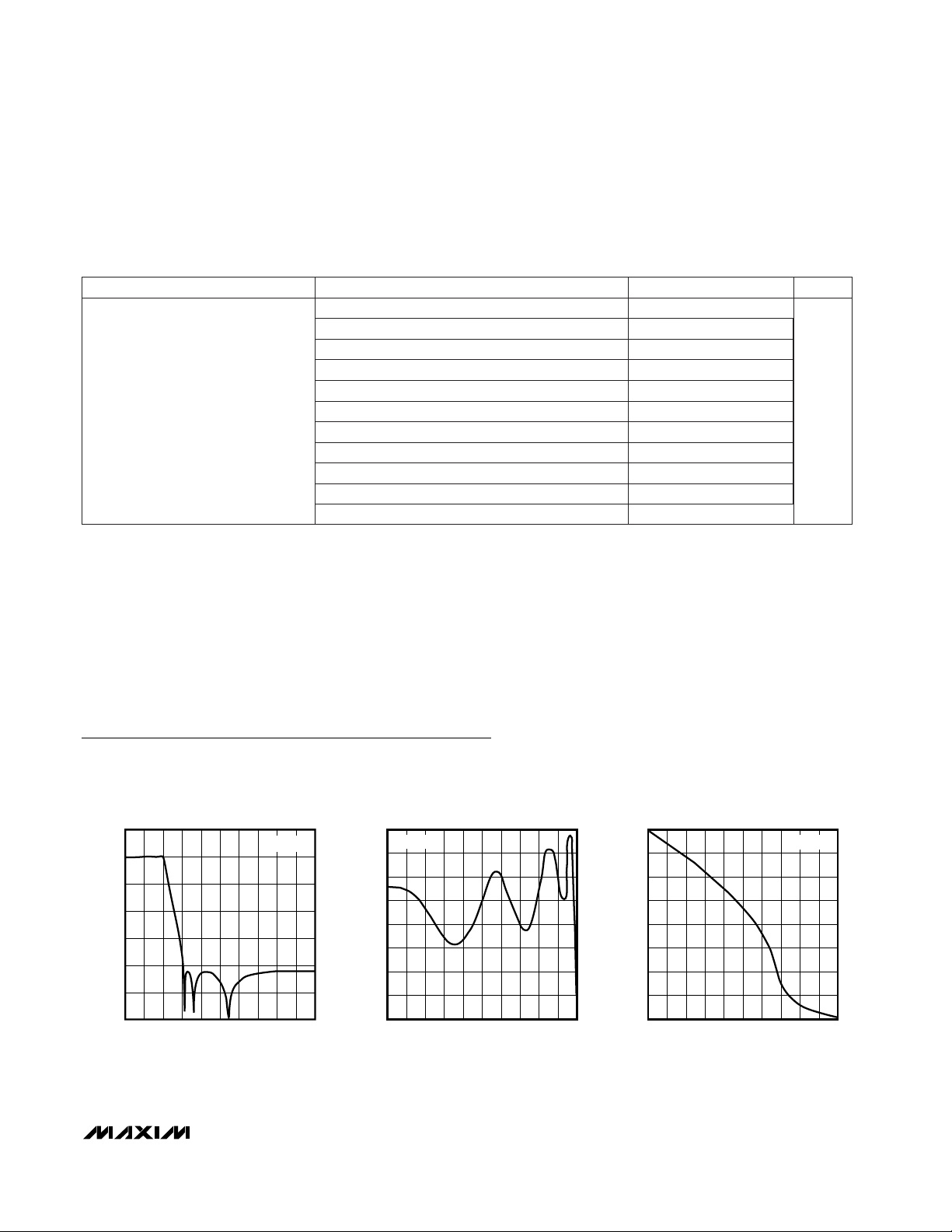
Typical Operating Characteristics
(VDD= +5V for MAX7400/MAX7403, VDD= +3V for MAX7404/MAX7407; V
COM
= VOS= VDD/ 2; SHDN = VDD; f
CLK
= 100kHz;
T
A
= +25°C; unless otherwise noted.)
-120
-80
-100
-40
-60
0
-20
20
012345
MAX7400/MAX7404 (r = 1.5)
FREQUENCY RESPONSE
MAX7400/03-01
INPUT FREQUENCY (kHz)
GAIN (dB)
fC = 1kHz
-0.08
0
-0.04
0.12
0.08
0.04
0.20
0.16
0.24
0 202 404 606 808 1010
MAX7400/MAX7404 (r = 1.5)
PASSBAND FREQUENCY RESPONSE
MAX7400/03-02
INPUT FREQUENCY (Hz)
GAIN (dB)
fC = 1kHz
-640
-480
-560
-240
-320
-400
-80
-160
0
0 300 600 900 1200 1500
MAX7400/MAX7404 (r = 1.5)
PHASE RESPONSE
MAX7400/03-03
INPUT FREQUENCY (Hz)
PHASE SHIFT (DEGREES)
fC = 1kHz
PARAMETER MIN TYP MAX UNITS
-58 -50
-60 -54
Insertion Gain Relative to DC Gain
(Note 5)
-60 -54
fIN= 1.533f
C
dB
fIN= 2.875f
C
-59 -54
fIN= 1.200f
C
fIN= 1.261f
C
-0.20 0.10 0.20
-0.20 0.14 0.30
CONDITIONS
-0.20 0.09 0.30
fIN= 0.992f
C
fIN= 1.000f
C
-0.20 0.02 0.20
fIN= 0.902f
C
fIN= 0.956f
C
-0.20 0.02 0.20
-0.20 -0.06 0.20
fIN= 0.640f
C
fIN= 0.784f
C
-0.20 -0.11 0.20fIN= 0.408f
C
MAX7400/MAX7403/MAX7404/MAX7407
Page 6
MAX7400/MAX7403/MAX7404/MAX7407
8th-Order, Lowpass, Elliptic,
Switched-Capacitor Filters
6 _______________________________________________________________________________________
Typical Operating Characteristics (continued)
(VDD= +5V for MAX7400/MAX7403, VDD= +3V for MAX7404/MAX7407; V
COM
= VOS= VDD/ 2; SHDN = VDD; f
CLK
= 100kHz;
T
A
= +25°C; unless otherwise noted.)
1.5
1.8
1.7
1.6
1.9
2.0
2.1
2.2
2.3
2.4
2.5
2.5 3.53.0 4.0 4.5 5.0 5.5
SUPPLY CURRENT
vs. SUPPLY VOLTAGE
MAX7400 toc07
SUPPLY VOLTAGE (V)
SUPPLY CURRENT (mA)
NO LOAD
MAX7404
MAX7407
MAX7400
MAX7403
1.97
1.99
1.98
2.01
2.00
2.02
2.03
-40 20 40-20 0 60 80 100
SUPPLY CURRENT
vs. TEMPERATURE
MAX7400 toc08
TEMPERATURE (°C)
SUPPLY CURRENT (mA)
NO LOAD
MAX7400
MAX7403
MAX7404
MAX7407
-20
-15
-10
-5
0
5
10
15
20
2.5 3.53.0 4.0 4.5 5.0 5.5
OFFSET VOLTAGE
vs. SUPPLY VOLTAGE
MAX7400 toc09
SUPPLY VOLTAGE (V)
OFFSET VOLTAGE (mV)
VIN = V
COM
= VDD/2
MAX7404
MAX7407
MAX7400
MAX7403
-0.5
0
0.5
1.5
1.0
2.0
-40 -20 0 20 40 60 80 100
OFFSET VOLTAGE vs. TEMPERATURE
MAX7400/03-10
TEMPERATURE (°C)
OFFSET VOLTAGE (mV)
VIN = V
COM
= VDD/2
-90
-70
-80
-50
-60
-40
-30
-10
-20
0
012345
THD PLUS NOISE vs. INPUT SIGNAL
AMPLITUDE (MAX7400)
MAX7400/03 11
AMPLITUDE (Vp-p)
THD + NOISE (dB)
NO LOAD
(SEE TABLE A)
B
C
D
-90
-70
-80
-50
-60
-40
-30
-10
-20
0
012345
THD PLUS NOISE vs. INPUT SIGNAL
AMPLITUDE AND RESISTIVE LOAD (MAX7400)
MAX7400/03-12
AMPLITUDE (Vp-p)
THD + NOISE (dB)
fIN = 200Hz
f
C
= 1kHz
MEASUREMENT BW = 22kHz
RL = 500Ω
RL = 1kΩ
RL = 10kΩ
-120
-80
-100
-60
0
20
-20
-40
40
012345
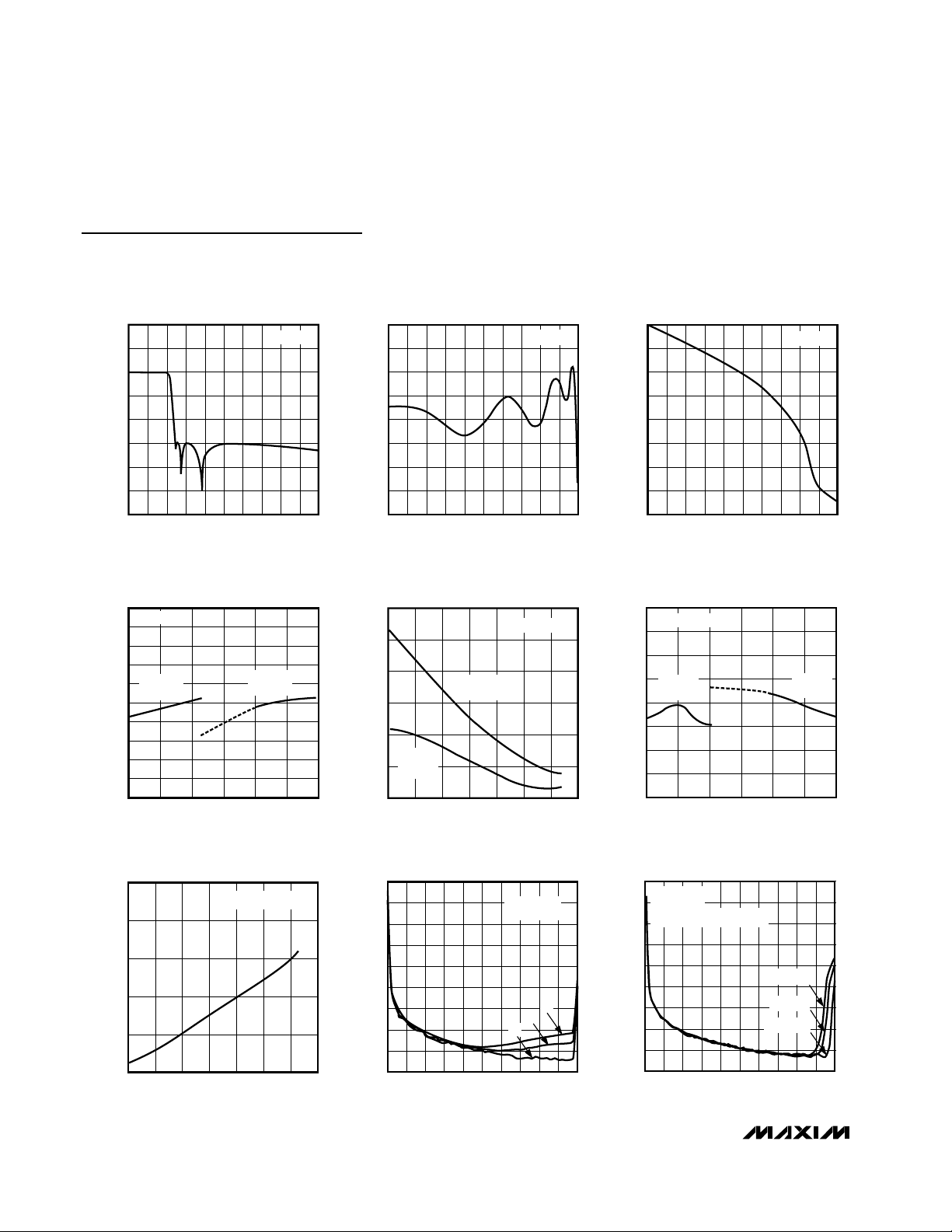
MAX7403/MAX7407 (r = 1.2)
FREQUENCY RESPONSE
MAX7400/03 04
INPUT FREQUENCY (kHz)
GAIN (dB)
fC = 1kHz
-0.32
-0.16
-0.24
-0.08
0.16
0.24
0.08
0
0.32
0 202 404 606 808 1010
MAX7403/MAX7407 (r = 1.2)
PASSBAND FREQUENCY RESPONSE
MAX7400/03 05
INPUT FREQUENCY (Hz)
GAIN (dB)
fC = 1kHz
-640
-480
-560
-400
-160
-80
-240
-320
0
0 240 480 720 960 1200
MAX7403/MAX7407 (r = 1.2)
PHASE RESPONSE
MAX7400/03 06
INPUT FREQUENCY (Hz)
PHASE SHIFT (DEGREES)
fC = 1kHz
Page 7
MAX7400/MAX7403/MAX7404/MAX7407
8th-Order, Lowpass, Elliptic,
Switched-Capacitor Filters
_______________________________________________________________________________________
7
-90
-70
-80
-50
-60
-40
-30
-10
-20
0
012345
THD PLUS NOISE vs. INPUT SIGNAL
AMPLITUDE (MAX7403)
MAX7400/03 13
AMPLITUDE (Vp-p)
THD + NOISE (dB)
NO LOAD
(SEE TABLE A)
B
C
D
-90
-70
-80
-50
-60
-40
-30
-10
-20
0
012345
THD PLUS NOISE vs. INPUT SIGNAL
AMPLITUDE AND RESISTIVE LOAD (MAX7403)
TABLE A. THD PLUS NOISE vs. INPUT SIGNAL
AMPLITUDE TEST CONDITIONS
MAX7400/03 14
AMPLITUDE (Vp-p)
THD + NOISE (dB)
fIN = 200Hz
f
C
= 1kHz
MEASUREMENT BW = 22kHz
RL = 500Ω
R
L =
1kΩ
RL = 10kΩ
TRACE
f
IN
(Hz)
f
C
(kHz)
f
CLK
(kHz)
MEASUREMENT
BANDWIDTH (kHz)
A
B
C
2800
2000
1000
14
10
5
1400
1000
500
80
80
80
D 200 1 100 22
Typical Operating Characteristics (continued)
(VDD= +5V for MAX7400/MAX7403, VDD= +3V for MAX7404/MAX7407; V
COM
= VOS= VDD/ 2; SHDN = VDD; f
CLK
= 100kHz;
T
A
= +25°C; unless otherwise noted.)
-90
-70
-80
-40
-50
-60
-10
-20
-30
0
0 1.00.5 1.5 2.0 2.5 3.0
THD PLUS NOISE vs. INPUT SIGNAL
AMPLITUDE AND RESISTIVE LOAD (MAX7404)
MAX7400 toc16
AMPLITUDE (Vp-p)
THD + NOISE (dB)
RL = 10kΩ
RL = 1kΩ
RL = 500Ω
fIN = 200Hz
f
C
= 1kHz
MEASUREMENT BW = 22kHz
-90
-70
-80
-40
-50
-60
-10
-20
-30
0
0 1.00.5 1.5 2.0 2.5 3.0
THD PLUS NOISE vs. INPUT SIGNAL
AMPLITUDE (MAX7407)
MAX 7400 toc17
AMPLITUDE (Vp-p)
THD + NOISE (dB)
NO LOAD
(SEE TABLE A)
A
B
C
D
-90
-70
-80
-40
-50
-60
-10
-20
-30
0
0 1.00.5 1.5 2.0 2.5 3.0
THD PLUS NOISE vs. INPUT SIGNAL
AMPLITUDE AND RESISTIVE LOAD (MAX7407)
MAXX7400 toc18
AMPLITUDE (Vp-p)
THD + NOISE (dB)
RL = 500Ω
fIN = 200Hz
f
C
= 1kHz
MEASUREMENT BW = 22kHz
RL = 10kΩ
RL = 1kΩ
-90
-70
-80
-40
-50
-60
-10
-20
-30
0
0 1.00.5 1.5 2.0 2.5 3.0
THD PLUS NOISE vs. INPUT SIGNAL
AMPLITUDE (MAX7404)
MAX7400 toc15
AMPLITUDE (Vp-p)
THD + NOISE (dB)
B
NO LOAD
(SEE TABLE A)
C
D
A
Page 8

Pin Description
PIN
Common Input. Biased internally at midsupply. Bypass externally to GND with a 0.1µF capacitor. To override internal biasing, drive with an external supply.
COM1
FUNCTIONNAME
Filter InputIN2
Positive Supply Input: +5V for MAX7400/MAX7403, +3V for MAX7404/MAX7407V
DD
4
GroundGND3
Offset Adjust Input. To adjust output offset, bias OS externally. Connect OS to COM if no offset adjustment is
needed. Refer to
Offset and Common-Mode Input Adjustment
section.
OS6
Clock Input. To override the internal oscillator, connect to an external clock; otherwise, connect an external
capacitor (C
OSC
) from CLK to GND to set the internal oscillator frequency.
CLK8
Shutdown Input. Drive low to enable shutdown mode; drive high or connect to VDDfor normal operation.
SHDN
7
Filter OutputOUT5
MAX7400/MAX7403/MAX7404/MAX7407
8th-Order, Lowpass, Elliptic,
Switched-Capacitor Filters
8 _______________________________________________________________________________________
Typical Operating Characteristics (continued)
(VDD= +5V for MAX7400/MAX7403, VDD= +3V for MAX7404/MAX7407; V
COM
= VOS= VDD/ 2; SHDN = VDD; f
CLK
= 100kHz;
T
A
= +25°C; unless otherwise noted.)
0.96
0.98
0.97
1.00
0.99
1.03
1.02
1.01
1.04
-40 0-20 20 40 60 80 100
NORMALIZED OSCILLATOR FREQUENCY
vs. TEMPERATURE
MAX7400 toC21
TEMPERATURE (°C)
NORMALIZED OSCILLATOR FREQUENCY
C
OSC
= 390pF
MAX7400
MAX7403
MAX7404
MAX7407
0.80
0.85
0.90
0.95
1.00
1.05
1.10
1.15
1.20
2.5 3.53.0 4.0 4.5 5.0 5.5
NORMALIZED OSCILLATOR FREQUENCY
vs. SUPPLY VOLTAGE
MAX7400 toc20
SUPPLY VOLTAGE (V)
NORMALIZED OSCILLATOR FREQUENCY
C
OSC
= 390pF
MAX7400
MAX7403
MAX7404
MAX7407
0.1
1
100
10
1000
10,000
0.0110.1
10
100
1000
INTERNAL OSCILLATOR FREQUENCY
vs. C
OSC
CAPACITANCE
MAX7400 toc19
C
OSC
CAPACITANCE (nF)
OSCILLATOR FREQUENCY (kHz)
Page 9
MAX7400/MAX7403/MAX7404/MAX7407
8th-Order, Lowpass, Elliptic,
Switched-Capacitor Filters
_______________________________________________________________________________________ 9
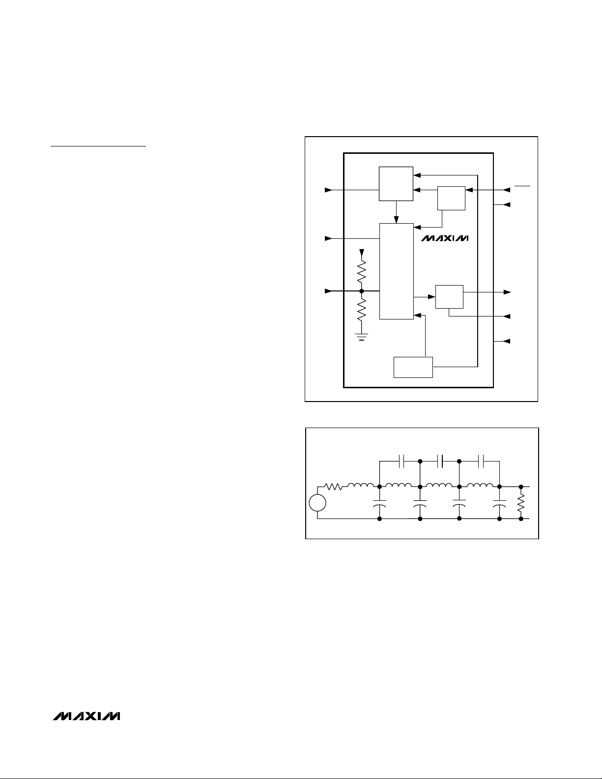
Detailed Description
The MAX7400/MAX7403/MAX7404/MAX7407 family of
8th-order, lowpass filters provides sharp rolloff with
good stopband rejection. All parts operate with a
100:1 clock-to-corner frequency ratio and a 10kHz
maximum corner frequency. These devices accept a
single +5V (MAX7400/MAX7403) or +3V (MAX7404/
MAX7407) supply. Figure 1 shows the functional diagram.
Most switched-capacitor filters (SFCs) are designed
with biquadratic sections. Each section implements two
filtering poles, and the sections can be cascaded to
produce higher-order filters. The advantage of this
approach is ease of design. However, this type of
design is highly sensitive to component variations if any
section’s Q is high. The MAX7400 family uses an alternative approach, which is to emulate a passive network
using switched-capacitor integrators with summing and
scaling. The passive network can be synthesized using
CAD programs or can be found in many filter books.
Figure 2 shows a basic 8th-order ladder elliptic filter
structure.
A switched-capacitor filter that emulates a passive ladder filter retains many of the same advantages. The
component sensitivity of a passive ladder filter is low
when compared to a cascaded biquadratic design,
because each component affects the entire filter shape
rather than a single pole-zero pair. In other words, a
mismatched component in a biquadratic design has a
concentrated error on its respective poles, while the
same mismatch in a ladder filter design spreads its
error over all poles.
Elliptic Characteristics
Lowpass, elliptic filters such as the MAX7400/MAX7403/
MAX7404/MAX7407 provide the steepest possible rolloff
with frequency of the four most common filter types
(Butterworth, Bessel, Chebyshev, and Elliptic). Figure 3
shows the 8th-order elliptic filter response. The high Q
value of the poles near the passband edge combined
with the stopband zeros allows for the sharp attenuation characteristic of elliptic filters, making these
devices ideal for anti-aliasing and post-DAC filtering in
single-supply systems (see the
Anti-Aliasing and Post-
DAC Filtering
section).
In the frequency domain, the first transmission zero
causes the filter’s amplitude to drop to a minimum level.
Beyond this zero, the response rises as the frequency
increases until the next transmission zero. The stopband
begins at the stopband frequency, fS. At frequencies
above fS, the filter’s gain does not exceed the gain at fS.
The corner frequency, f
C
, is defined as the point where
the filter output attenuation falls just below the passband
ripple. The transition ratio is defined as the ratio of the
stopband frequency to the corner frequency:
r = fS/ f
C
The MAX7400/MAX7404 have a transition ratio of 1.5
and a typical stopband rejection of 82dB. The
MAX7403/MAX7407 have a transition ratio of 1.2 (providing the steepest rolloff) and a typical stopband
rejection of 60dB.
2
INT
CLOCK
IN
1
COM
8
CLK
SHDN
7
4
5
6
3
V
DD
OUT
OS
GND
BIAS
SCF
LOGIC
OFFSET
ADJ
MAX7400
MAX7403
MAX7404
MAX7407
V
DD
Figure 1. Functional Diagram
C10
C11
C9
L3
L5 L7
C8
R2
C4C2
V
IN
+
-
V
0
L1
R1
C6
Figure 2. 8th-Order Ladder Filter Network
Page 10

V
DD
V
SUPPLY
IN
CLK
GND
INPUT
OUTPUT
50k
50k
50k
OUT
0.1µF
0.1µF
0.1µF
CLOCK
SHDN
COM
OS
MAX7400
MAX7403
MAX7404
MAX7407
Figure 4. Offset Adjustment Circuit
MAX7400/MAX7403/MAX7404/MAX7407
8th-Order, Lowpass, Elliptic,
Switched-Capacitor Filters
10 ______________________________________________________________________________________
Clock Signal
External Clock
The MAX7400/MAX7403/MAX7404/MAX7407 SCFs
were designed for use with external clocks that have a
40% to 60% duty cycle. When using an external clock,
drive CLK with a CMOS gate powered from 0 to VDD.
Varying the rate of the external clock adjusts the filter
corner frequency:
fC= f
CLK
/ 100
Internal Clock
When using the internal oscillator, the capacitance
(C
OSC
) on the CLK pin determines the oscillator fre-
quency:
where K = 38 for the MAX7400/MAX7403, and K = 34
for the MAX7404/MAX7407. Since the capacitor value
is in picofarads, minimize the stray capacitance at CLK
so that it does not affect the internal oscillator frequency. Varying the rate of the internal oscillator adjusts the
filter’s corner frequency by a 100:1 clock-to-corner frequency ratio. For example, an internal oscillator frequency of 100kHz produces a nominal corner
frequency of 1kHz.
Input Impedance
vs. Clock Frequencies
The MAX7400/MAX7403/MAX7404/MAX7407’s input
impedance is effectively that of a switched-capacitor
resistor and is inversely proportional to frequency. The
input impedance determined by the following equation
represents the average input impedance, since the
input current is not continuous. As a rule, use a driver
with an output source impedance less than 10% of the
filter’s input impedance. Estimate the input impedance
of the filter using the following formula:
where f
CLK
=clock frequency and CIN=0.85pF.
Low-Power Shutdown Mode
These devices feature a shutdown mode that is activated by driving SHDN low. Placing the filter in shutdown
mode reduces the supply current to 0.2µA (typ) and
places the output of the filter into a high-impedance
state. For normal operation, drive SHDN high or connect to VDD.
Applications Information
Offset and Common-Mode
Input Adjustment
The voltage at COM sets the common-mode input voltage and is internally biased at midsupply by a resistordivider. Bypass COM with a 0.1µF capacitor and
connect OS to COM. For applications requiring offset
adjustment or DC level shifting, apply an external bias
voltage through a resistor-divider network to OS, as
shown in Figure 4. (Note: Do not leave OS unconnected.) The output voltage is represented by the following
equation:
V
OUT
= (VIN- V
COM
) + V
OS
Z
fC
IN
CLK IN
()
( )
Ω=
⋅
1
f (kHz) =
K 10
C
OSC
3
OSC
⋅
; CinpF
OSC
PASSBAND STOPBAND
GAIN (dB)
FREQUENCY
f
CfS
f
S
f
C
f
S
f
C
TRANSITION RATIO =
RIPPLE
Figure 3. Elliptic Filter Response
Page 11
MAX7400/MAX7403/MAX7404/MAX7407
8th-Order, Lowpass, Elliptic,
Switched-Capacitor Filters
______________________________________________________________________________________ 11
with V
COM
= VDD/ 2 (typical), and where (VIN- V
COM
)
is lowpass filtered by the SCF, and VOSis added at the
output stage. See the
Electrical Characteristics
for
COM and OS input voltage ranges. Changing the voltage on COM or OS significantly from midsupply
reduces the filter’s dynamic range.
Power Supplies
The MAX7400/MAX7403 operate from a single +5V
supply. The MAX7404/MAX7407 operate from a single
+3V supply. Bypass VDDto GND with a 0.1µF capacitor. If dual supplies are required, connect COM to the
system ground and GND to the negative supply. Figure
5 shows an example of dual-supply operation. Singlesupply and dual-supply performance are equivalent.
For single-supply or dual-supply operation, drive CLK
and SHDN from GND (V- in dual-supply operation) to
VDD. For a ±2.5V supply, use the MAX7400 or MAX7403;
for a ±1.5V supply, use MAX7404 or MAX7407. For ±5V
dual-supply applications, use the MAX291–MAX297.
Input Signal Amplitude Range
The ideal input signal range is determined by observing the voltage level at which the total harmonic
distortion plus noise (THD+N) is minimized for a given
corner frequency. The
Typical Operating Character-
istics
show THD+N response as the input signal’s
peak-to-peak amplitude is varied. These measurements
are made with OS and COM biased at midsupply.
Anti-Aliasing and Post-DAC Filtering
When using the MAX7400/MAX7403/MAX7404/
MAX7407 for anti-aliasing or post-DAC filtering, synchronize the DAC and the filter clocks. If the clocks are
not synchronized, beat frequencies may alias into the
passband.
The high clock-to-corner frequency ratio (100:1) also
eases the requirements of pre- and post-SCF filtering.
At the input, a lowpass filter prevents the aliasing of frequencies around the clock frequency into the passband. At the output, a lowpass filter attenuates the
clock feedthrough.
A high clock-to-corner frequency ratio allows a simple
RC lowpass filter, with the cutoff frequency set above
the SCF corner frequency, to provide input anti-aliasing
and reasonable output clock attenuation.
Harmonic Distortion
Harmonic distortion arises from nonlinearities within the
filter. Such nonlinearities generate harmonics when a
pure sine wave is applied to the filter input. Table 1 lists
typical harmonic distortion values with a 10kΩ load and
an input signal of 4Vp-p (MAX7400/MAX7403) or 2Vp-p
(MAX7404/MAX7407), at TA= +25°C.
V
DD
V+
V-
IN
CLK
GND
INPUT
OUTPUTOUT
0.1µF
CLOCK
*DRIVE SHDN TO V- FOR LOW-POWER SHUTDOWN MODE.
SHDN
COM
OS
0.1µF
MAX7400
MAX7403
MAX7404
MAX7407
*
V+
V-
Figure 5. Dual-Supply Operation
2nd
-88100
TYPICAL
HARMONIC
DISTORTION (dB)
1
f
C
(kHz)
-89100
200
1
-84
f
IN
(Hz)
200
4th3rd 5th
-89500
MAX7400
5 1000
-86-89-82
-88-93-77
500
MAX7403
5 1000
-87-91
FILTER
-81
-91-90-80
4
V
IN
(Vp-p)
4
f
CLK
(kHz)
-85100 1 200
-85500
MAX7404
5 1000
-86-85-82
-84-86-81
2
-85100 1 200
-86500
MAX7407
5 1000
-86-85-82
-86-85-84
2
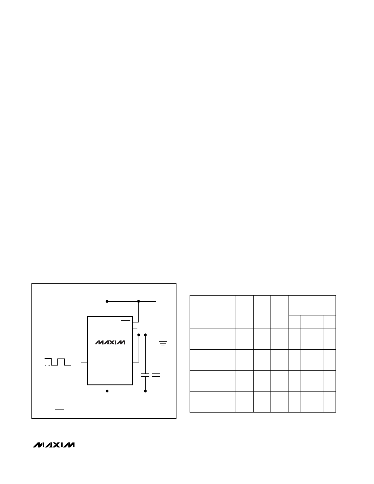
Table 1. Typical Harmonic Distortion
Page 12

MAX7400/MAX7403/MAX7404/MAX7407
8th-Order, Lowpass, Elliptic,
Switched-Capacitor Filters
Package Information
SOICN.EPS
TRANSISTOR COUNT: 1116
Ordering Information (continued) Chip Information
PART
MAX7403CSA
MAX7403CPA
MAX7403ESA -40°C to +85°C
0°C to +70°C
0°C to +70°C
TEMP. RANGE PIN-PACKAGE
8 SO
8 Plastic DIP
8 SO
MAX7403EPA -40°C to +85°C 8 Plastic DIP
MAX7404CSA
MAX7404CPA
MAX7404ESA -40°C to +85°C
0°C to +70°C
0°C to +70°C 8 SO
8 Plastic DIP
8 SO
MAX7404EPA -40°C to +85°C 8 Plastic DIP
MAX7407CSA
MAX7407CPA
MAX7407ESA -40°C to +85°C
0°C to +70°C
0°C to +70°C 8 SO
8 Plastic DIP
8 SO
MAX7407EPA -40°C to +85°C 8 Plastic DIP
Maxim cannot assume responsibility for use of any circuitry other than circuitry entirely embodied in a Maxim product. No circuit patent licenses are
implied. Maxim reserves the right to change the circuitry and specifications without notice at any time.
12
____________________Maxim Integrated Products, 120 San Gabriel Drive, Sunnyvale, CA 94086 408-737-7600
© 1999 Maxim Integrated Products Printed USA is a registered trademark of Maxim Integrated Products.
 Loading...