

Page 1
General Description
The MAX7393/MAX7394 precision silicon oscillators
replace crystals, ceramic resonators, and crystal oscillator
modules in systems with a +2.4V to +3.6V operating supply voltage range.
The MAX7393/MAX7394 consist of a temperature-compensated precision oscillator with enable (MAX7394) or
autoenable (MAX7393). The MAX7393/MAX7394 are supplied at specific frequencies, just like crystals and resonators. Output frequency accuracy is guaranteed to be
within ±0.25% (TDFN) and ±1.3% (µDFN) (0°C to +85°C)
and ±1.0% (TDFN) and ±1.8% (µDFN) over the -40°C to
+125°C temperature range.
The small size and robust operation of the MAX7393/
MAX7394 make them ideal for space-constrained or environmentally demanding applications where high accuracy is required. The high accuracy of the MAX7393/
MAX7394 is ideal for use in USB applications, computers,
and white goods.
The MAX7393/MAX7394 are available in 6-pin, 3mm x
3mm TDFN and 2mm x 2mm µDFN packages. They are
specified for the -40°C to +125°C temperature range.
Applications
Features
♦ ±0.25% (TDFN) and ±1.3% (µDFN) Total Accuracy
for 0°C to +85°C
♦ ±1.0% (TDFN) and ±1.8% (µDFN) Total Accuracy
for -40°C to +125°C
♦ Resistant to Humidity and Vibration
♦ 12mA Operating Current (48MHz Version)
♦ 5ns Output Rise/Fall Time
♦ 40% to 60% Maximum Duty Cycle
♦ No External Components Required
♦ +2.4V to +3.6V Operation
♦ Available Factory-Set Frequencies from 922kHz to
48MHz
♦ Space-Saving TDFN and µDFN Surface-Mount
Packages
MAX7393/MAX7394
Precision Silicon Oscillators with
Enable or Autoenable
________________________________________________________________ Maxim Integrated Products 1
Ordering Information
19-3876; Rev 0; 5/06
For pricing, delivery, and ordering information, please contact Maxim/Dallas Direct! at
1-888-629-4642, or visit Maxim’s website at www.maxim-ic.com.
*The two-letter frequency suffix following the part number is found
in the Selector Guide.
+Denotes lead-free package.
Note: The MAX7394 is available in factory-set frequencies from
922kHz to 48MHz. The MAX7393 is available in factory-set
frequencies from 922kHz to 20MHz. There are 10 standard
frequencies (see the Selector Guide) with a required 2.5k order
increment. Nonstandard frequencies are also available with a
required 10k order increment. For nonstandard versions,
contact factory for availability and ordering information.
USB
CAN Nodes
Automotive Systems
Computers
Handheld Products
White Goods
Selector Guide and Pin Configurations appear at end of
data sheet.
Typical Application Circuits
2.4V TO 3.6V
6
V
V
V
CC
CC
CC2
MAX7393
GNDI.C.
23
2.4V TO 3.6V
6
V
CC2
1
1
CLOCK
CLKIN
CLOCK
5
OSC1
4
OSC2
5
OSC1
µC
µC
PA R T * T EM P RA N G E
M A X7 3 9 3 ALT_ _+ - 40°C to + 125°C 6 µD FN L622- 1
M AX 7393ATT_ _+ - 40°C to + 125°C 6 TD FN T633- 1
M A X7 3 9 4 ALT_ _+ - 40°C to + 125°C 6 µD FN L622- 1
M AX 7394ATT_ _+ - 40°C to + 125°C 6 TD FN T633- 1
PIN -
PA C K A G E
PK G
C O D E
MAX7394
4
ENABLE
GNDI.C.
23
OSC2
Page 2
MAX7393/MAX7394
Precision Silicon Oscillators with
Enable or Autoenable
2 _______________________________________________________________________________________
ABSOLUTE MAXIMUM RATINGS
ELECTRICAL CHARACTERISTICS
(VCC= V
CC2
= +2.4V to +3.6V, CL= 10pF, TA= -40°C to +125°C, unless otherwise noted. Typical values are at VCC= V
CC2
= +3.3V,
T
A
= +25°C, unless otherwise noted.) (Note 1)
Stresses beyond those listed under “Absolute Maximum Ratings” may cause permanent damage to the device. These are stress ratings only, and functional
operation of the device at these or any other conditions beyond those indicated in the operational sections of the specifications is not implied. Exposure to
absolute maximum rating conditions for extended periods may affect device reliability.
VCC, V
CC2
to GND.................................................-0.3V to +4.0V
CLOCK, CLKIN, ENABLE, I.C. to GND ......-0.3V to (V
CC
+ 0.3V)
CLOCK Output Current ....................................................±50mA
Continuous Power Dissipation (T
A
= +70°C)
6-Pin µDFN (derate 4.5mW/°C over +70°C) ................358mW
6-Pin TDFN (derate 18.2mW/°C over +70°C) ............1455mW
Operating Temperature Range .........................-40°C to +125°C
Junction Temperature......................................................+150°C
Storage Temperature Range .............................-65°C to +150°C
Lead Temperature (soldering, 10s) .................................+300°C
DC CHARACTERISTICS
Operating Supply Voltage V
Operating Output Supply Voltage V
Total Operating Supply Current
(Note 2)
Total Shutdown Supply Current I
LOGIC INPUTS (ENABLE, CLKIN)
Logic Input High Voltage V
Logic Input Low Voltage V
CLOCK OUTPUT
Output High Voltage V
Output Low Voltage V
Output Rise Time t
Output Fall Time t
Duty Cycle (Note 3) 47 %
Startup Time Time for output to stabilize 2 ms
Output Jitter (Note 3)
PARAMETER SYMBOL CONDITIONS MIN TYP MAX UNITS
CC
CC2
I
TOT
SHDN
IH
IL
OH
OL
R
F
922kHz, MAX739_ _ _ _LY 4.4
4MHz, MAX739_ _ _ _RD 5.4
8MHz, MAX739_ _ _ _TP 5.8
16MHz, MAX739_ _ _ _WB 6.5
32MHz, MAX7394_ _ _ YN 9.2
33MHz, MAX7394_ _ _ YQ 9.5
48MHz, MAX7394_ _ _ ZY 12
Oscillator disabled,
CLKIN = high (MAX7393),
ENABLE = low (MAX7394) (Note 2)
V
≥ 2.4V, I
CC2
V
≥ 2.4V, I
CC2
(Note 3) 5 ns
(Note 3) 5 ns
Peak-to-peak jitter, 16MHz (MAX7394) 180
Peak-to-peak jitter, 48MHz (MAX7394) 140
2.4 3.6 V
2.4 3.6 V
12µA
0.7
x V
CC2
0.3
x V
CC2
V
= 5mA
SOURCE
= 5mA 0.3 V
SINK
CC2
- 0.3
mA
V
V
V
ps
Page 3
MAX7393/MAX7394
Precision Silicon Oscillators with
Enable or Autoenable
_______________________________________________________________________________________ 3
Note 1: All parameters are production tested at TA= +25°C. Specifications over temperature are guaranteed by design and
characterization.
Note 2: The total supply current is the sum of I
CC
and I
CC2
.
Note 3: Guaranteed by design and characterization. Not production tested.
Note 4: Output frequency is production tested at T
A
= +25°C and TA= +85°C.
Note 5: Output frequency is production tested at T
A
= +25°C.
ELECTRICAL CHARACTERISTICS (continued)
(VCC= V
CC2
= +2.4V to +3.6V, CL= 10pF, TA= -40°C to +125°C, unless otherwise noted. Typical values are at VCC= V
CC2
= +3.3V,
T
A
= +25°C, unless otherwise noted.) (Note 1)
FREQUENCY ACCURACY
Clock Frequency Coefficient of
Temperature
Clock Frequency Coefficient of
Supply Voltage
Total Accuracy V
PARAMETER SYMBOL CONDITIONS MIN TYP MAX UNITS
TA = 0°C to +70°C ±20
T
= -40°C to +125°C ±50
A
T
= 0°C to
A
+ 85°C ,
V
= ± 10%
C C
= - 40°C
T
A
to + 125° C ,
V
= ± 10%
C C
TD FN
( N ote 4)
µD FN
( N ote 5)
TD FN
( N ote 4)
µD FN
( N ote 5)
= V
= V
C C 2
C C 2
= 3.3V
= 3.3V
V
C C
= +25°C 0.1 0.15 %/V
T
A
C C
±0.25
±1.3
±1.0
±1.8
ppm/°C
%
Page 4

MAX7393/MAX7394
Precision Silicon Oscillators with
Enable or Autoenable
4 _______________________________________________________________________________________
Typical Operating Characteristics
(VCC= V
CC2
= 3.3V, TA= +25°C, MAX7394, 48MHz output, unless otherwise noted.)
60
58
56
54
52
50
48
DUTY CYCLE (%)
46
44
42
40
DUTY CYCLE vs. TEMPERATURE
MAX7393/4 toc01
-40 -25 -10 5 20 35 50 65 80 95 110 125
TEMPERATURE (°C)
DUTY CYCLE vs. SUPPLY VOLTAGE
60
58
56
54
52
50
48
DUTY CYCLE (%)
46
44
42
40
2.4 2.6 2.8 3.0 3.2 3.4 3.6
SUPPLY VOLTAGE (V)
10
V
9
MAX7393/4 toc01
8
7
6
5
4
3
TOTAL SUPPLY CURRENT (mA)
2
1
0
-40 -25 -10 5 20 35 50 65 80 95 110 125
TOTAL SUPPLY CURRENT
vs. TEMPERATURE
= V
= +3.6V
CC
CC2
VCC = V
= +3.3V
CC2
TEMPERATURE (°C)
VCC = V
CC2
MAX7393/4 toc03
= +2.4V
TOTAL SUPPLY CURRENT
vs. SUPPLY VOLTAGE
10
8
6
4
TOTAL SUPPLY CURRENT (mA)
2
0
2.4 2.6 2.8 3.0 3.2 3.4 3.6
SUPPLY VOLTAGE (V)
9
8
7
6
5
4
3
2
TOTAL SUPPLY CURRENT (mA)
1
0
0 6 12 18 24 30 36 42 48
1.000
MAX7393 toc04
0.999
0.998
0.997
NORMALIZED FREQUENCY
0.996
0.995
2.4 2.6 2.8 3.0 3.2 3.4 3.6
TOTAL SUPPLY CURRENT
vs. FREQUENCY
VCC = V
= +3.6V
CC2
VCC = V
= +3.3V
CC2
VCC = V
FREQUENCY (MHz)
NORMALIZED FREQUENCY
vs. SUPPLY VOLTAGE
SUPPLY VOLTAGE (V)
MAX7393 toc07
= +2.4V
CC2
NORMALIZED FREQUENCY
1.002
1.000
MAX7393/4 toc05
0.998
0.996
0.994
NORMALIZED FREQUENCY
0.992
0.990
-40 -25 -10 5 20 35 50 65 80 95 110 125
MAX7393 SETTLING TIME FROM START
(SEE FIGURE 1)
20MHz
400µs/div
MAX7393 toc08
vs. TEMPERATURE
TEMPERATURE (°C)
ON/OFF
2V/div
CLOCK
2V/div
MAX7393/4 toc06
Page 5

MAX7393/MAX7394
Precision Silicon Oscillators with
Enable or Autoenable
_______________________________________________________________________________________ 5
Pin Description
Typical Operating Characteristics (continued)
(VCC= V
CC2
= 3.3V, TA= +25°C, MAX7394, 48MHz output, unless otherwise noted.)
MAX7394 SETTLING TIME FROM START
MAX7393 toc09
ENABLE
2V/div
CLOCK OUTPUT WAVEFORM
WITH C
= 10pF
L
MAX7393 toc10
CLOCK
2V/div
400µs/div
PIN
MAX7393 MAX7394
11V
2 2 GND Ground
3 3 I.C.
4 — CLKIN
5 5 CLOCK Clock Output. CLOCK is a rail-to-rail, push-pull output.
66V
— 4 ENABLE
——EP
NAME FUNCTION
CC
CC2
Positive Supply Voltage Input. Bypass VCC to GND with 0.1µF capacitors placed as close to
the device as possible. Connect V
Internally Connected. Connect I.C. to GND. Do not connect I.C. to any other input or output.
Do not leave I.C. unconnected.
Clock Input. Connect CLKIN to a returned clock signal source (see the Autoenable (CLKIN,
MAX7393) section).
Positive Supply Voltage Input for Output Driver. Bypass V
placed as close to the device as possible. Connect V
Enable Input. Drive ENABLE low to place the MAX7394 in shutdown mode. Drive ENABLE
high for normal operation.
Exposed Paddle, TDFN Version Only. Connect EP to ground. Do not connect EP to any other
input or output.
CC
to V
CC2
10ns/div
.
CLOCK
1V/div
to GND with a 0.1µF capacitor
CC2
to VCC.
CC2
Page 6

MAX7393/MAX7394
Detailed Description
The MAX7393/MAX7394 precision silicon oscillators
replace crystals, ceramic resonators, and crystal oscillator modules in systems with a +2.4V to +3.6V operating
supply voltage range. The MAX7393/MAX7394 consist of
a temperature-compensated precision oscillator with
enable (MAX7394) or autoenable (MAX7393). The
ENABLE input on the MAX7394 manually enables or disables the oscillator. The CLKIN input on the MAX7393
monitors a returned clock signal to automatically enable
or disable the MAX7393 oscillator.
The MAX7393/MAX7394 are supplied at specific frequencies, like crystals and resonators. A variety of popular
standard frequencies are available (see the Selector
Guide). Output frequency accuracy is guaranteed to be
within ±0.25% (TDFN) and ±1.3% (µDFN) (0°C to +85°C)
and ±1.0% (TDFN) and ±1.8% (µDFN) over the -40°C to
+125°C temperature range. No external components are
required to generate the specific frequency.
ENABLE (MAX7394)
The ENABLE input on the MAX7394 turns the oscillator
on and off. Drive ENABLE to a logic-high for normal
operation. Drive ENABLE to a logic-low to place the
device in shutdown mode. During shutdown, the oscillator is turned off, and the CLOCK output is weakly driven
high with an internal 10kΩ to V
CC2
. In shutdown mode,
the total supply current reduces to less than 2µA.
Autoenable (CLKIN, MAX7393)
The MAX7393 features a CLKIN input that automatically
enables or disables the oscillator by sensing the condition of a returned clock signal. The MAX7393 is automatically enabled whenever an active inversion function
is sensed between CLOCK and CLKIN. When no inversion function is detected, the MAX7393 automatically
enters shutdown mode. During shutdown, the oscillator
is turned off, the CLKIN input is weakly driven to its last
state, and the CLOCK output is weakly driven to the
logic-level in CLKIN.
The CLKIN input relies on an external inversion function, typically provided by a microcontroller’s clock
generator, to provide an inverted version of the CLOCK
output signal. The MAX7393 interprets high/low voltage
or a constant high-impedance node on CLKIN as a
disable signal.
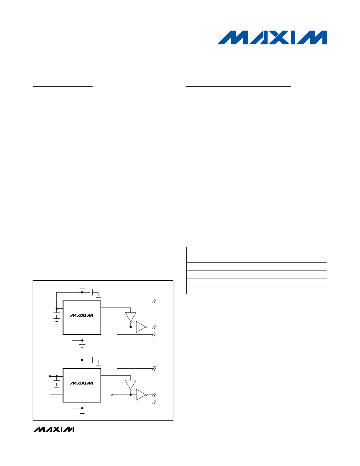
Figure 1 shows a test circuit to enable or disable the
MAX7393. One input of the NAND gate connects to the
CLOCK output of the MAX7393, and the other input is
driven with a logic level. A logic-high level enables the
oscillator and a logic-low level disables the oscillator.
See the Typical Operating Characteristics for typical
startup performance of the MAX7393.
Oscillator (CLOCK)
The CLOCK output is a push-pull, CMOS logic output
that is capable of driving a ground-connected 1kΩ load
or a positive supply connected 500Ω load to within
300mV of either supply rail. There are no impedancematching issues when using the MAX7393/MAX7394
CLOCK output. A typical startup characteristic is shown
in the Typical Operating Characteristics.
Output Jitter
The MAX7393/MAX7394s’ jitter performance is given in the
Electrical Characteristics table as a peak-to-peak value.
Applications Information
Interfacing to a Microcontroller
Clock Input
The MAX7393/MAX7394 CLOCK output is a push-pull,
CMOS logic output that directly drives any microprocessor (µP) or microcontroller (µC) clock input. There
are no impedance-matching issues when using the
MAX7393/MAX7394. Operate the MAX7393/MAX7394
and microcontroller from the same supply voltage level of
V
CC2
(see the Power-Supply Considerations section for
more details). Refer to the microcontroller’s data sheet for
clock input compatibility with external clock signals.
The MAX7393/MAX7394 require no biasing components or load capacitance. When using the MAX7393/
MAX7394 to retrofit a crystal oscillator, remove all biasing components from the oscillator input.
Power-Supply Considerations
The MAX7393/MAX7394 operate with power-supply
voltages in the +2.4V to +3.6V range. Connect V
CC
and
V
CC2
to the same supply voltage level as the device
receiving the clock. Proper power-supply decoupling is
required to maintain the power-supply rejection performance of the MAX7393/MAX7394. Connect 0.1µF
surface-mount ceramic capacitors from V
CC
to V
CC2
to
GND. Position these bypass capacitors as close to V
CC
and V
CC2
as possible.
A larger V
CC2
bypass capacitor value is recommended
if the MAX7393/MAX7394 are to operate with a large
capacitive load. Use a bypass capacitor value on V
CC2
at least 1000 times that of the output load capacitance.
Precision Silicon Oscillators with
Enable or Autoenable
6 _______________________________________________________________________________________
Figure 1. Test Circuit to Enable or Disable the MAX7393 Oscillator
CLOCK
MAX7393
CLKIN
ON/OFF
Page 7

MAX7393/MAX7394
Precision Silicon Oscillators with
Enable or Autoenable
_______________________________________________________________________________________ 7
Pin Configurations
Selector Guide
Chip Information
PROCESS: BiCMOS
TOP VIEW OF
BOTTOM LEADS
V
CLOCK CLKIN
CC2
456
MAX7393
123
+
V
GND I.C.
CC
µDFN
V
CLOCK CLKIN
CC2
6
54
*EP
MAX7393
+
123
V
GND I.C.
CC
*EXPOSED PADDLE. CONNECT EP TO GROUND.
+
TDFN
V
CLOCK ENABLE
CC2
456
MAX7394
123
V
GND I.C.
CC
µDFN
V
CLOCK ENABLE
CC2
6
54
*EP
PART F R EQ U ENC YPA CK A G ET O P M A RK
M AX 7393ATTLY 922kH z6 TD FN + AN P
M AX 7393ALTLY 922kH z6 µD FN + ABO
M AX 7393ATTM G1M H z6 TD FN + AN Q
M AX 7393ALTM G1M H z6 µD FN + ABP
M AX 7393ATTRD 4M H z6 TD FN + AN R
M AX 7393ALTRD 4M H z6 µD FN + ABQ
M AX 7393ATTTP 8M H z6 TD FN + AN S
M AX 7393ALTTP 8M H z6 µD FN + ABR
M AX 7393ATTWB 16M H z6 TD FN + AM N
M AX 7393ALTWB 16M H z6 µD FN + AAR
M AX 7393ATTWV 20M H z6 TD FN + AM O
M AX 7393ALTWV 20M H z6 µD FN + AAS
M AX 7394ATTLY 922kH z6 TD FN + AN V
M AX 7394ALTLY 922kH z6 µD FN + ABU
M AX 7394ATTM G1M H z6 TD FN + AN W
M AX 7394ALTM G1M H z6 µD FN + ABV
M AX 7394ATTRD 4M H z6 TD FN + AN X
M AX 7394ALTRD 4M H z6 µD FN + ABW
M AX 7394ATTTP 8M H z6 TD FN + AN Y
M AX 7394ALTTP 8M H z6 µD FN + ABX
M AX 7394ATTWB 16M H z6 TD FN + AM U
M AX 7394ALTWB 16M H z6 µD FN + AAY
M AX 7394ATTWV 20M H z6 TD FN + AM V
M AX 7394ALTWV 20M H z6 µD FN + AAZ
M AX 7394ATTY N 32M H z6 TD FN + AN Z
M AX 7394ALTY N 32M H z6 µD FN + ABY
M AX 7394ATTY Q 33M H z6 TD FN + AM X
M AX 7394ALTY Q 33M H z6 µD FN + ABB
M AX 7394ATTZ H 40M H z6 TD FN + AO A
M AX 7394ALTZ H 40M H z6 µD FN + ABZ
M AX 7394ATTZ Y 48M H z6 TD FN + AM Z
M AX 7394ALTZ Y 48M H z6 µD FN + ABD
MAX7394
+
123
V
GND I.C.
CC
*EXPOSED PADDLE. CONNECT EP TO GROUND.
TDFN
Page 8
MAX7393/MAX7394
Precision Silicon Oscillators with
Enable or Autoenable
8 _______________________________________________________________________________________
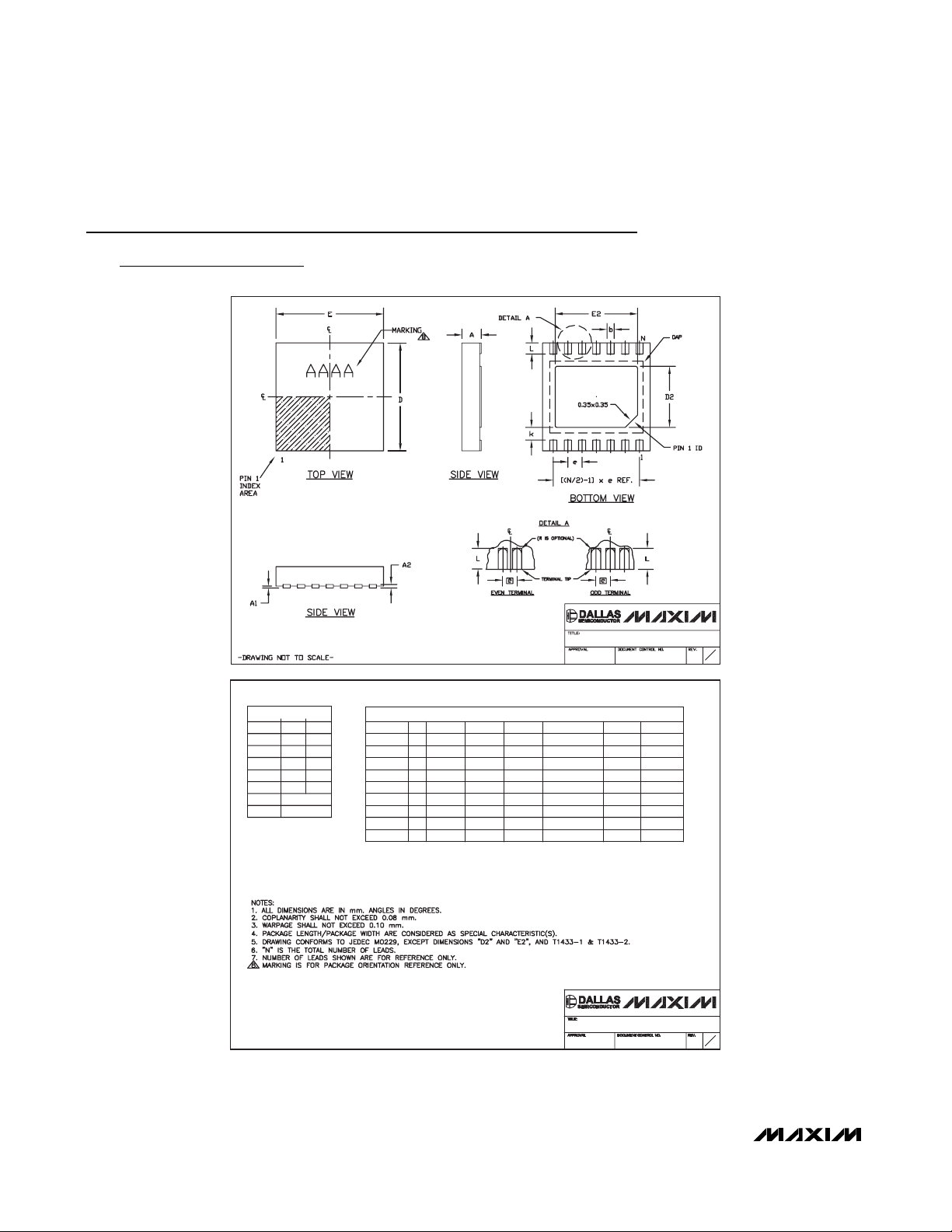
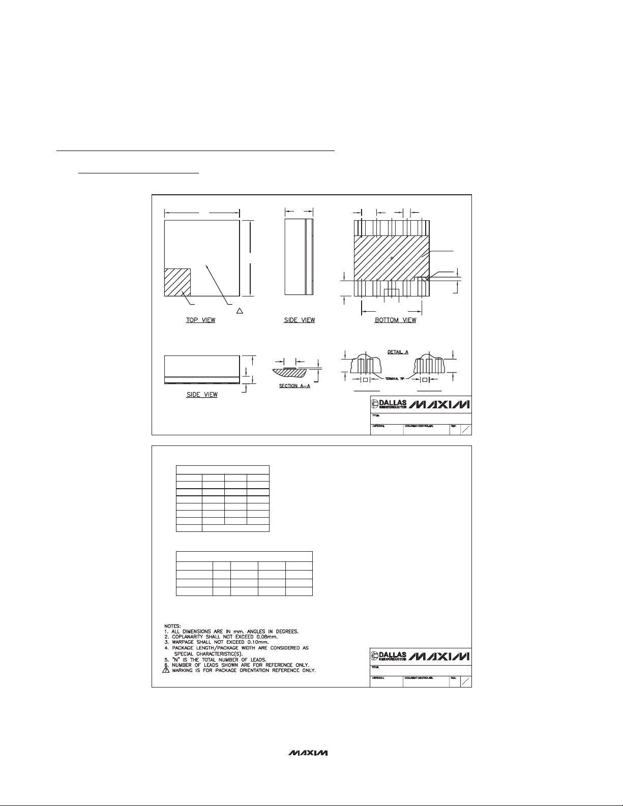
Package Information
(The package drawing(s) in this data sheet may not reflect the most current specifications. For the latest package outline information,
go to www.maxim-ic.com/packages
.)
6, 8, &10L, DFN THIN.EPS
COMMON DIMENSIONS
MIN. MAX.
SYMBOL
A 0.70 0.80
D 2.90 3.10
E 2.90 3.10
A1
0.00 0.05
L 0.20 0.40
0.25 MIN.k
A2 0.20 REF.
-DRAWING NOT TO SCALE-
PACKAGE OUTLINE, 6,8,10 & 14L,
TDFN, EXPOSED PAD, 3x3x0.80 mm
PACKAGE VARIATIONS
PKG. CODE N D2 E2 e JEDEC SPEC b [(N/2)-1] x e
T633-2 6 1.50±0.10 2.30±0.10
T833-2 8 1.50±0.10 2.30±0.10 0.65 BSC MO229 / WEEC 0.30±0.05 1.95 REF
T833-3 8 1.50±0.10 2.30±0.10 0.65 BSC MO229 / WEEC 0.30±0.05 1.95 REF
2.30±0.101.50±0.106T633-1 0.95 BSC MO229 / WEEA 1.90 REF0.40±0.05
2.30±0.10
0.95 BSC MO229 / WEEA
MO229 / WEEC
MO229 / WEED-3
MO229 / WEED-3
0.50 BSC
0.40 BSC - - - - 0.20±0.05 2.40 REFT1433-2 14 2.30±0.101.70±0.10
1.50±0.10
1.50±0.10
1.50±0.1010T1033-2
PACKAGE OUTLINE, 6,8,10 & 14L,
TDFN, EXPOSED PAD, 3x3x0.80 mm
21-0137
0.40±0.05 1.90 REF
1.95 REF0.30±0.050.65 BSC2.30±0.108T833-1
2.00 REF0.25±0.050.50 BSC2.30±0.1010T1033-1
2.00 REF0.25±0.05
2.40 REF0.20±0.05- - - - 0.40 BSC1.70±0.10 2.30±0.1014T1433-1
21-0137
1
H
2
2
H
2
Page 9
MAX7393/MAX7394
Precision Silicon Oscillators with
Enable or Autoenable
Maxim cannot assume responsibility for use of any circuitry other than circuitry entirely embodied in a Maxim product. No circuit patent licenses are
implied. Maxim reserves the right to change the circuitry and specifications without notice at any time.
Maxim Integrated Products, 120 San Gabriel Drive, Sunnyvale, CA 94086 408-737-7600 _____________________ 9
© 2006 Maxim Integrated Products Printed USA is a registered trademark of Maxim Integrated Products, Inc.
Package Information (continued)
(The package drawing(s) in this data sheet may not reflect the most current specifications. For the latest package outline information,
go to www.maxim-ic.com/packages
.)
Springer
-DRAWING NOT TO SCALE-
D
XXXX
XXXX
XXXX
PIN 1
INDEX AREA
SAMPLE
MARKING
7
A1
A
E
b
A
A2
L
L
e
C
L
e
EVEN TERMINAL
b
A A
(N/2 -1) x e)
PACKAGE OUTLINE,
6, 8, 10L uDFN, 2x2x0.80 mm
21-0164
N
1
C
L
e
ODD TERMINAL
SOLDER
MASK
COVERAGE
PIN 1
0.10x45∞
L1
L
1
A
2
6, 8, 10L UDFN.EPS
COMMON DIMENSIONS
SYMBOL MIN. NOM.
A
0.70 0.75
0.15 0.20 0.25
A1
A2
0.020 0.025 0.035
D 1.95 2.00
1.95 2.00
E
L
0.30 0.40
L1
PACKAGE VARIATIONS
PKG. CODE N e b
-DRAWING NOT TO SCALE-
6L622-1 0.65 BSC 0.30±0.05
0.10 REF.
MAX.
0.80
2.05
-
2.05
0.50
(N/2 -1) x e
1.30 REF.
0.25±0.050.50 BSC8L822-1
1.50 REF.
0.20±0.030.40 BSC10L1022-1
1.60 REF.
PACKAGE OUTLINE,
6, 8, 10L uDFN, 2x2x0.80 mm
21-0164
2
A
2
 Loading...