

Page 1
General Description
The MAX7375 is a silicon oscillator, intended as a lowcost improvement to replace ceramic resonators, crystals, and crystal oscillator modules used as the clock
source for microcontrollers and UARTs in 3V, 3.3V, and
5V applications.
The MAX7375 is a fully integrated oscillator, supplied at
specific factory-trimmed frequencies with a Rail-toRail® 50% duty cycle square-wave output. The oscillator frequency is generated directly without the use of a
phase-locked loop (PLL). No additional components
are used for setting or adjusting the frequency.
Unlike typical crystal and ceramic resonator oscillator
circuits, the MAX7375 is resistant to vibration and EMI.
The high output drive current and absence of highimpedance nodes make the oscillator less susceptible
to dirty or humid operating conditions. With a wide
operating temperature range, the oscillator is a good
choice for demanding home appliance and automotive
environments.
The MAX7375 is offered in space-saving 3-pin SC70
and SOT23 packages. All parts are guaranteed to operate over the -55°C to +135°C temperature range and
are specified from -40°C to +125°C.
Applications
White Goods Portable Equipment
Automotive Microcontroller Systems
Appliances and Controls
Hand-Held Products
Features
♦ 2.7V to 5.5V Operation
♦ Factory-Trimmed Oscillator
♦ No External Components Required
♦ ±10mA Output Drive Current
♦ 2% Initial Accuracy
♦ ±50ppm/°C Temp Drift
♦ Fast Startup Time: 5µs
♦ 45% to 55% Maximum Duty Cycle
♦ 5ns Output Rise and Fall Time
♦ No PLL
♦ Low Jitter: 160ps
P-P
at 8MHz
♦ Tiny Surface-Mount Package (SC70, SOT23)
♦ -40°C to +125°C Temperature Range
MAX7375
3-Pin Silicon Oscillator
________________________________________________________________ Maxim Integrated Products 1
Ordering Information
19-3060; Rev 0; 10/03
For pricing, delivery, and ordering information, please contact Maxim/Dallas Direct! at
1-888-629-4642, or visit Maxim’s website at www.maxim-ic.com.
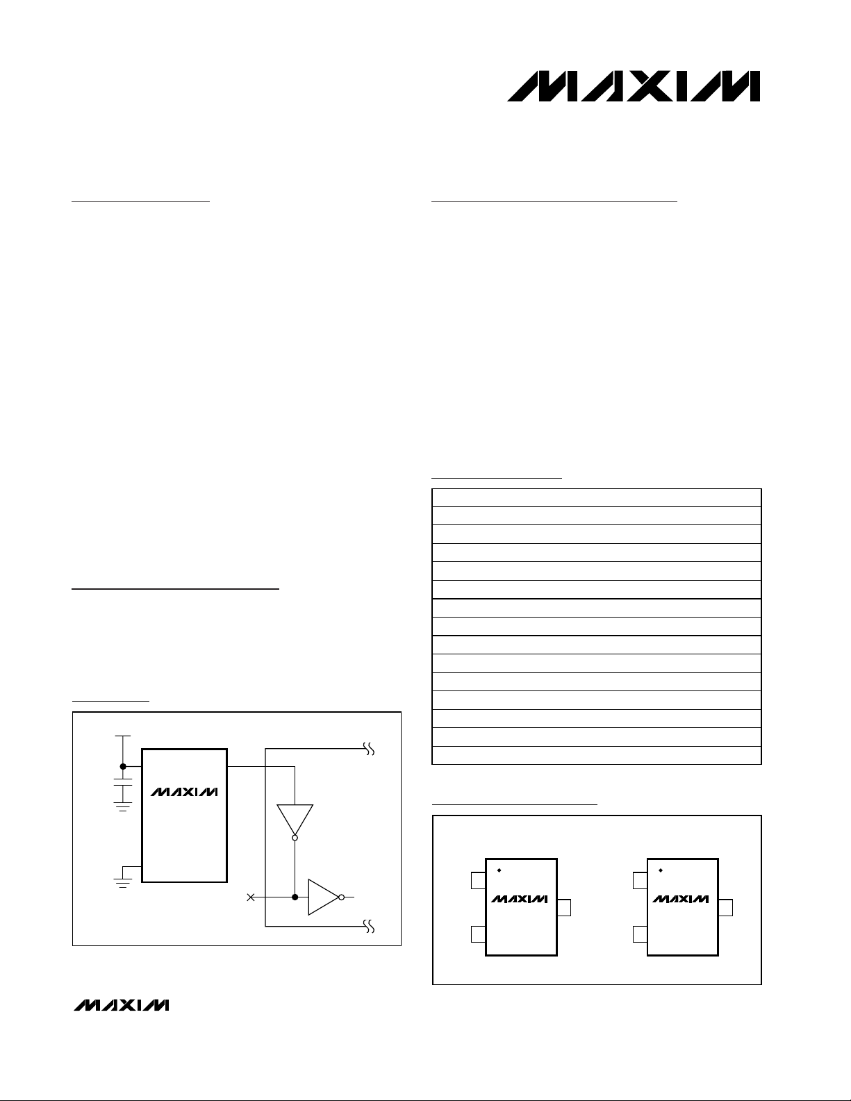
Pin Configuration
MAX7375
OSC1
OSC2
2.7V TO 5.5V
V+
GND
CLOCK
µC
Typical Application Circuit
Selector Guide appears at end of data sheet.
Rail-to-Rail is a registered trademark of Nippon Motorola, Ltd,
*Future product—contact factory for availability.
PART TEMP RANGE PIN-PACKAGE
MAX7375AXR105-T* -40°C to +125°C 3 SC70-3
MAX7375AXR185-T* -40°C to +125°C 3 SC70-3
MAX7375AXR365-T -40°C to +125°C 3 SC70-3
MAX7375AXR375-T -40°C to +125°C 3 SC70-3
MAX7375AXR405-T -40°C to +125°C 3 SC70-3
MAX7375AXR425-T -40°C to +125°C 3 SC70-3
MAX7375AXR805-T -40°C to +125°C 3 SC70-3
MAX7375AUR105-T* -40°C to +125°C 3 SOT23-3
MAX7375AUR185-T* -40°C to +125°C 3 SOT23-3
MAX7375AUR365-T -40°C to +125°C 3 SOT23-3
MAX7375AUR375-T -40°C to +125°C 3 SOT23-3
MAX7375AUR405-T -40°C to +125°C 3 SOT23-3
MAX7375AUR425-T -40°C to +125°C 3 SOT23-3
MAX7375AUR805-T -40°C to +125°C 3 SOT23-3
TOP VIEW
1
V+
CLOCK
MAX7375AXR
2V+
SC70
3 GND
CLOCK
1
MAX7375AUR
2
SOT23
3 GND
Page 2
MAX7375
3-Pin Silicon Oscillator
2 _______________________________________________________________________________________
ABSOLUTE MAXIMUM RATINGS
ELECTRICAL CHARACTERISTICS
(V+ = 2.7V to 5.5V, TA= -40°C to +125°C, unless otherwise noted. Typical values are at V+ = 5V, TA= +25°C.) (Note 1)
Stresses beyond those listed under “Absolute Maximum Ratings” may cause permanent damage to the device. These are stress ratings only, and functional
operation of the device at these or any other conditions beyond those indicated in the operational sections of the specifications is not implied. Exposure to
absolute maximum rating conditions for extended periods may affect device reliability.
Note 1: All parameters are tested at TA= +25°C. Specifications over temperature are guaranteed by design and characterization.
Note 2: Typical frequencies are nominal values.
Note 3: Guaranteed by design and characterization. Not production tested.
V+ to GND ................................................................-0.3V to +6V
CLOCK to GND ............................................-0.3V to (V+ + 0.3V)
Continuous Power Dissipation (T
A
= +70°C)
3-Pin SC70 (derate 2.9mW/°C over +70°C).................235mW
3-Pin SOT23 (derate 4mW/°C over +70°C...................320mW
Operating Temperature Range .........................-40°C to +125°C
Functional Temperature Range .........................-55°C to +135°C
Junction Temperature......................................................+150°C
Storage Temperature Range .............................-65°C to +150°C
Lead Temperature (soldering, 10s) .................................+300°C
Operating Supply Voltage V+ 2.7 5.5 V
Operating Supply Current I
Output High Voltage V
Output Low Voltage V
Initial CLOCK Frequency f
CLOCK Frequency Temperature
Sensitivity
Duty Cycle (Note 3) 45 52 57 %
Output Jitter
Output Rise Time t
Output Fall Time t
PARAMETER SYMBOL CONDITIONS MIN TYP MAX UNITS
MAX7375A_R405 2.0 4.2
+
MAX7375A_R805 3.2 6.4
OH
OL
CLOCK
R
F
V+ ≥ 2.7V, I
V+ ≥ 4.5V, I
V+ ≥ 2.7, I
V+ ≥ 4.5V, I
V+ = 3.0V,
T
A
V+ = 2.7V to 5.5V,
T
A
(Note 3) ±50 ±325 ppm/°C
Observation for 20s using a 500MHz
oscilloscope (MAX7375A_R805)
(Note 3) 5.0 ns
(Note 3) 2.5 ns
SINK
= +25°C (Note 2)
= +25°C (Note 2)
= 2.5mA V+ - 0.4
SOURCE
= 9mA V+ - 0.4
SOURCE
= 10mA 0.4
= 20mA 0.4
SINK
MAX7375A_R_
MAX7375A_R_
_ _ -2% +2%
_ _ -4% +4%
160 ps
V
V
V
MHz
P-P
Page 3
MAX7375
3-Pin Silicon Oscillator
_______________________________________________________________________________________ 3
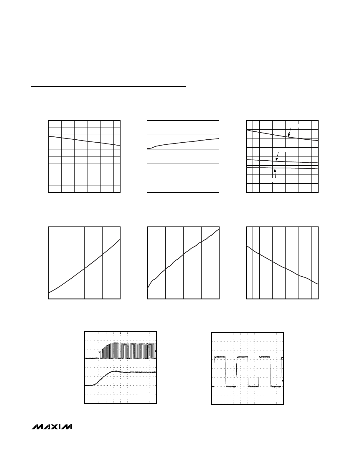
Typical Operating Characteristics
(V+ = 5V, TA= +25°C, CL= 10pF, 8MHz output, unless otherwise noted.)
DUTY CYCLE vs. TEMPERATURE
55
54
53
52
51
50
49
DUTY CYCLE (%)
48
47
46
45
-40 125
TEMPERATURE (°C)
SUPPLY CURRENT vs. SUPPLY VOLTAGE
4.0
3.5
3.0
MAX7375 toc01
1109565 80-10 5 20 35 50-25
MAX7375 toc04
DUTY CYCLE vs. SUPPLY VOLTAGE
55
53
51
49
DUTY CYCLE (%)
47
45
2.7 5.5
SUPPLY VOLTAGE (V)
FREQUENCY vs. SUPPLY VOLTAGE
1.002
1.000
0.998
SUPPLY CURRENT vs. TEMPERATURE
4.0
3.5
MAX7375 toc02
3.0
2.5
2.0
1.5
SUPPLY CURRENT (mA)
1.0
0.5
4.84.13.4
0
-40 125
V+ = 2.7V
TEMPERATURE (°C)
FREQUENCY vs. TEMPERATURE
1.010
MAX7375 toc05
1.005
V+ = 5V
MAX7375 toc03
V+ = 3.3V
1109565 80-10 5 20 35 50-25
MAX7375 toc06
2.5
2.0
SUPPLY CURRENT (mA)
1.5
1.0
2.7 5.5
SUPPLY VOLTAGE (V)
SETTLING TIME FROM START
0.996
0.994
NORMALIZED FREQUENCY
0.992
4.84.13.4
0.990
2.7 5.5
SUPPLY VOLTAGE (V)
4.84.13.4
1.000
NORMALIZED FREQUENCY
0.995
0.990
-40 125
TEMPERATURE (°C)
1109565 80-10 5 20 35 50-25
CLOCK OUTPUT WAVEFORM
= 10pF
WITH C
L
40ns/div
MAX7375 toc08
V+ = 3.3V
CLOCK
1V/div
1µs/div
MAX7375 toc07
V+ = 3.3V
CLOCK
2V/div
V+
2V/div
Page 4

MAX7375
Detailed Description
The MAX7375 is a replacement for ceramic resonators,
crystals, and crystal oscillator modules as the clock
source for microcontrollers and UARTs in 3V, 3.3V, and
5V applications. The MAX7375 is an integrated oscillator, supplied at specific frequencies just like crystals
and resonators. A variety of popular standard frequencies are available. No external components are
required for setting or adjusting the frequency.
Supply Voltages
The MAX7375 has been designed for use in systems
with nominal supply voltages of 3V, 3.3V, or 5V and is
specified for operation with supply voltages in the 2.7V
to 5.5V range. Operation outside this range is not guaranteed. See the Absolute Maximum Ratings table for
limit values of power-supply and pin voltages.
Oscillator
The clock output is a push-pull configuration and is
capable of driving a ground-connected 1kΩ load or a
positive supply connected 500Ω load to within 300mV
of either supply rail. The clock output remains stable
over the full operating voltage range and does not generate short output cycles during either power on or
power off. A typical startup characteristic is shown in
the Typical Operating Characteristics section.
Output Jitter
The MAX7375’s jitter performance is given in the
Electrical Characteristics table as a peak-to-peak value
obtained by observing the output of the MAX7375 for
20s with a 500MHz oscilloscope. Jitter measurements
are approximately proportional to the period of the output frequency of the device. Thus, a 4MHz part has
approximately twice the jitter value of an 8MHz part.
The jitter performance of all clock sources degrades in
the presence of mechanical and electrical interference.
The MAX7375 is relatively immune to vibration, shock,
and EMI influences and thus provides a considerably
more robust clock source than crystal- or ceramic-resonator-based oscillator circuits.
3-Pin Silicon Oscillator
4 _______________________________________________________________________________________
Pin Description
Typical Operating Characteristics (continued)
(V+ = 5V, TA= +25°C, CL= 10pF, 8MHz output, unless otherwise noted.)
CLOCK OUTPUT WAVEFORM
WITH C
L
= 50pF
MAX7375 toc09
40ns/div
CLOCK
1V/div
V+ = 3.3V
CLOCK OUTPUT WAVEFORM
WITH C
L
= 100pF
MAX7375 toc10
40ns/div
CLOCK
1V/div
V+ = 3.3V
PIN
SC70 SOT23
1 2 V+ Positive Supply Voltage
2 1 CLOCK Clock output. Output is push-pull.
3 3 GND Ground
NAME FUNCTION
Page 5

Applications Information
Interfacing to a Microcontroller Clock
Input
The MAX7375 clock output is a push-pull, CMOS, logic
output, which directly drives any microprocessor (µP)
or microcontroller (µC) clock input. There are no impedance-matching issues when using the MAX7375.
Operate the MAX7375 and microcontroller (or other
clock input device) from the same supply voltage level.
Refer to the microcontroller data sheet for clock input
compatibility with external clock signals.
The MAX7375 requires no biasing components or load
capacitance. When using the MAX7375 to retrofit a
crystal oscillator, remove all biasing components from
the oscillator input.
Startup Performance
The MAX7375 oscillator output stabilizes within a few
cycles of operation after V+ rises to a sufficient voltage
to start the oscillator, typically 1.65V at +25°C. Use a
reset or similar voltage-detection circuit to disable
devices connected to the MAX7375 until 5µs after the
voltage on V+ has risen above 2.7V.
Power-Supply Considerations
The MAX7375 operates with power-supply voltages in
the 2.7V to 5.5V range. Good power-supply decoupling
is needed to maintain the power-supply rejection performance of the MAX7375. Use a 0.1µF surface-mount
ceramic capacitor connected between V+ and GND
and mounted as close to the device as possible. If possible, mount the MAX7375 close to the microcontroller’s
decoupling capacitor so that additional decoupling is
not required.
A larger value of bypass capacitor is recommended if
the MAX7375 is to operate with a large capacitive load.
Use a bypass capacitor value of at least 1000 times
that of the output load capacitance.
Chip Information
TRANSISTOR COUNT: 432
PROCESS: BiCMOS
MAX7375
3-Pin Silicon Oscillator
_______________________________________________________________________________________ 5
Selector Guide
PART FREQUENCY (MHz) TOP MARK
MAX7375AXR105 1 AOV
MAX7375AXR185 1.8432 AOU
MAX7375AXR365 3.579545 AOT
MAX7375AXR375 3.6864 AOS
MAX7375AXR405 4 AOR
MAX7375AXR425 4.1943 AOQ
MAX7375AXR805 8 AOP
MAX7375AUR105 1 FZPZ
MAX7375AUR185 1.8432 FZPT
MAX7375AUR365 3.579545 FZPU
MAX7375AUR375 3.6864 FZPV
MAX7375AUR405 4 FZPY
MAX7375AUR425 4.1943 FZPW
MAX7375AUR805 8 FZPX
Page 6

Package Information
(The package drawing(s) in this data sheet may not reflect the most current specifications. For the latest package outline information,
go to www.maxim-ic.com/packages
.)
MAX7375
3-Pin Silicon Oscillator
6 _______________________________________________________________________________________
SC70, 3L.EPS
Page 7

MAX7375
3-Pin Silicon Oscillator
Maxim cannot assume responsibility for use of any circuitry other than circuitry entirely embodied in a Maxim product. No circuit patent licenses are
implied. Maxim reserves the right to change the circuitry and specifications without notice at any time.
Maxim Integrated Products, 120 San Gabriel Drive, Sunnyvale, CA 94086 408-737-7600 _____________________ 7
© 2003 Maxim Integrated Products Printed USA is a registered trademark of Maxim Integrated Products.
Package Information (continued)
(The package drawing(s) in this data sheet may not reflect the most current specifications. For the latest package outline information,
go to www.maxim-ic.com/packages
.)
SOT23 L.EPS
PACKAGE OUTLINE, 3L SOT-23
1
21-0051
F
1
 Loading...