

Page 1
MAX7360
AD0
PORT7
PORT6
PORT0
COL_(8x)
ROW_(8x)
INTK
INTI
SDA
SCL
ROTARY
SWITCH
+14V
8 x 8
TO
FC
+1.8V
19-4566; Rev 0; 4/09
EVALUATION KIT
AVAILABLE
I2C-Interfaced Key-Switch Controller and LED
Driver/GPIOs with Integrated ESD Protection
General Description
The MAX7360 I2C-interfaced peripheral provides microprocessors with management of up to 64 key switches,
with an additional eight LED drivers/GPIOs that feature
constant-current, PWM intensity control, and rotary
switch control options.
The key-switch drivers interface with metallic or resistive
switches with on-resistances up to 5kI. Key inputs
are monitored statically, not dynamically, to ensure
low-EMI operation. The MAX7360 features autosleep
and autowake modes to further minimize the power
consumption of the device. The autosleep feature puts
the device in a low-power state (1FA typ) after a sleep
timeout period. The autowake feature configures the
MAX7360 to return to normal operating mode from sleep
upon a keypress.
The key controller debounces and maintains a FIFO of
keypress and release events (including autorepeat, if
enabled). An interrupt (INTK) output can be configured
to alert keypresses, as they occur, or at maximum rate.
There are eight open-drain I/O ports, which can be used
to drive LEDs. The maximum constant-current level for
each open-drain port is 20mA. The intensity of the LED
on each open-drain port can be individually adjusted
through a 256-step PWM control. An input port pair
(PORT6, PORT7) can be configured to accept 2-bit gray
code inputs from a rotary switch. In addition, if not used
for key-switch control, up to six column pins can be used
as general-purpose open-drain outputs (GPOs) for LED
drive or logic control.
The MAX7360 is offered in a 40-pin (5mm x 5mm) thin
QFN package with an exposed pad, and a small 36-bump
wafer level package (WLP) for cell phones, pocket PCs,
and other portable consumer electronic applications. The
MAX7360 operates over the -40NC to +85NC extended
temperature range.
Applications
Cell Phones
PDAs
Handheld Games
Portable Consumer Electronics
Printers
Instrumentation
For pricing, delivery, and ordering information, please contact Maxim Direct at 1-888-629-4642,
or visit Maxim’s website at www.maxim-ic.com.
_______________________________________________________________ Maxim Integrated Products 1
Features
S Integrated ESD Protection
Q8kV IEC 61000-4-2 Contact Discharge
Q15kV IEC 61000-4-2 Air-Gap Discharge
S +14V Tolerant, Open-Drain I/O Ports Capable of
Constant-Current LED Drive
S Rotary Switch-Capable Input Pair (PORT6, PORT7)
S 256-Step PWM Individual LED Intensity Control
S Individual LED Blink Rates and Common LED
Fade In/Out Rates from 256ms to 4096ms
S FIFO Queues Up to 16 Debounced Key Events
S User-Configurable Key Debounce (9ms to 40ms)
S Keyscan Uses Static Matrix Monitoring for Low
EMI Operation
S +1.62V to +3.6V Operation
S Monitors Up to 64 Keys
S Key-Switch Interrupt (INTK) on Each Debounced
Event/FIFO Level, or End of Definable Time Period
S Port Interrupt (INTI) for Input Ports for Special-Key
Functions
S 400kbps, +5.5V Tolerant 2-Wire Serial Interface
with Selectable Bus Timeout
S Four I
2
C Address Choices
Ordering Information
PART TEMP RANGE PIN-PACKAGE
MAX7360ETL+ -40°C to +85°C 40 TQFN-EP*
MAX7360EWX+** -40°C to +85°C 36 WLP
+Denotes a lead(Pb)-free/RoHS-compliant package.
*EP = Exposed pad.
**Future product—contact factory for availability.
Simplfied Block Diagram
Pin Configurations appear at end of data sheet.
MAX7360
Page 2

I2C-Interfaced Key-Switch Controller and LED
Driver/GPIOs with Integrated ESD Protection
ABSOLUTE MAXIMUM RATINGS
VCC to GND ............................................................. -0.3V to +4V
COL0–COL7, ROW0–ROW7 to GND ......................-0.3V to +4V
SDA, SCL, AD0, INTI, INTK to GND ........................ -0.3V to +6V
PORT0–PORT7 to GND ......................................... -0.3V to +16V
All Other Pins to GND ................................-0.3V to (VCC + 0.3V)
DC Current on PORT0–PORT7, COL2–COL7 ....................25mA
GND Current .......................................................................80mA
Continuous Power Dissipation (TA = +70NC)
MAX7360
40-Pin TQFN (derate 22.2mW/NC above +70NC).......1777mW
36-Bump WLP (derate 21.7mW/NC above +70NC) .... 1739mW
Junction-to-Case Thermal Resistance (BJC) (Note 1)
40-Pin TQFN .................................................................. 2NC/W
36-Bump WLP ...................................................................N/A
Junction-to-Ambient Thermal Resistance (BJA) (Note 1)
40-Pin TQFN ................................................................ 45NC/W
36-Bump WLP .............................................................46NC/W
Note 1: Package thermal resistances were obtained using the method described in JEDEC specification JESD51-7, using a single layer board. For detailed information on package thermal considerations, refer to www.maxim-ic.com/thermal-tutorial.
Note 2: Refer to Pb-free solder-reflow requirements described in J-STD-020, Rev D.1, or any other paste supplier specification.
Stresses beyond those listed under “Absolute Maximum Ratings” may cause permanent damage to the device. These are stress ratings only, and functional operation of the device at these
or any other conditions beyond those indicated in the operational sections of the specifications is not implied. Exposure to absolute maximum rating conditions for extended periods may
affect device reliability.
Operating Temperature Range .......................... -40NC to +85NC
Junction Temperature .....................................................+150NC
Storage Temperature Range ............................ -65NC to +150NC
ESD Protection
Human Body Model (RD = 1.5kI, CS = 100pF)
All Pins .............................................................................Q2kV
IEC61000-4-2 (RD = 330I, CS = 150pF)
Contact Discharge
ROW0–ROW7, COL0–COL7, PORT0–PORT7 to GND ....Q8kV
Air-Gap Discharge
ROW0–ROW7, COL0–COL7, PORT0–PORT7 to GND ..Q15kV
Lead Temperature (soldering, 10s)
40-Pin TQFN ................................................................+300NC
36-Bump WLP ........................................................... (Note 2)
ELECTRICAL CHARACTERISTICS
(VCC = +1.62V to +3.6V, TA = -40NC to +85NC, unless otherwise noted. Typical values are at VCC = +3.3V, TA = +25NC.) (Notes 3, 4)
PARAMETER SYMBOL CONDITIONS MIN TYP MAX UNITS
Operating Supply Voltage V
External Supply Voltage
PORT0–PORT7
Operating Supply Current I
Sleep-Mode Supply Current I
Key-Switch Source Current I
Key-Switch Source Voltage V
Key-Switch Resistance R
Startup Time from Shutdown t
Output Low Voltage
COL2–COL7
Oscillator Frequency (PWM
Clock)
Oscillator Frequency Variation Df
Key-Scan Frequency f
V
CC
PORT_
CC
SL
KEY
KEY
KEY
START
V
OL
f
OSC
OSC
KEY
All key switches open, oscillator running,
COL2–COL7 configured as key switches,
V
_ = V
PORT
N keys pressed
(Note 5) 5 kI
I
SINK
TA = +25NC, VCC = +2.61V 125 128 131
TA = T
TA = +25NC -6 +8.5 %
Derived from oscillator clock 64 kHz
CC
= 10mA 0.5 V
- T
, V
MIN
MAX
P 3.6V 102 164
CC
1.62 3.3 3.6 V
14 V
34 50
FA
34 +
20 x N
1.3 3 FA
20 35 FA
0.43 0.5 V
2 2.4 ms
kHz
2 ______________________________________________________________________________________
Page 3

I2C-Interfaced Key-Switch Controller and LED
Driver/GPIOs with Integrated ESD Protection
ELECTRICAL CHARACTERISTICS (continued)
(VCC = +1.62V to +3.6V, TA = -40NC to +85NC, unless otherwise noted. Typical values are at VCC = +3.3V, TA = +25NC.) (Notes 3, 4)
PARAMETER SYMBOL CONDITIONS MIN TYP MAX UNITS
GPIO SPECIFICATIONS
Input High Voltage
PORT0–PORT7
Input Low Voltage
PORT0–PORT7
Input Leakage Current
PORT0–PORT7
Output Low Voltage
PORT0–PORT7
Input Capacitance
PORT0–PORT7
10mA Port Sinking Current
PORT0–PORT7
V
IH
V
IL
VIN P V
I
IN
V
OL
CC
VCC < V
I
VCC = +1.62V to +3.6V, TA = +25NC 8.55 11.52
VCC = +3.3V, VOL = +1V 8.67 9.76 10.51
IN
< 20mA 0.6 V
SINK
0.7 x
V
CC
0.3 x
V
CC
-0.25 +0.25
-1 +5
20 pF
V
V
FA
mA
MAX7360
20mA Port Sinking Current
PORT0–PORT7
Port Sink Current Variation
Output Logic-Low Voltage
INTI, INTK
PWM Frequency f
SERIAL-INTERFACE SPECIFICATIONS
Input High Voltage
SDA, SCL, AD0
Input Low Voltage
SDA, SCL, AD0
Input Leakage Current
SDA, SCL, AD0
Output Low Voltage
SDA
Input Capacitance
SDA, SCL, AD0
I2C TIMING SPECIFICATIONS
SCL Serial-Clock Frequency f
Bus Free Time Between a STOP
and START Condition
Hold Time (Repeated) START
Condition
Repeated START Condition
Setup Time
STOP Condition Setup Time t
PWM
V
C
t
t
HD, STA
t
SU, STA
SU, STO
V
IH
V
IL
I
IN
OL
IN
SCL
BUF
VCC = +1.62V to +3.6V, TA = +25NC 19.40 21.33
VCC = +3.3V, VOL = +1V 19.55 20 20.69
VCC = +3.3V, VOL = +1V, TA = +25NC,
20mA output mode
I
= 10mA 0.6 V
SINK
Derived from oscillator clock 500 Hz
0.7 x
V
VIN P V
CC
VIN > V
CC
I
= 6mA 0.6 V
SINK
Bus timeout disabled 0 400 kHz
-0.25 +0.25
-0.5 +0.5
1.3 Fs
0.6 Fs
0.6 Fs
0.6 Fs
+Q1.5 +Q2.4 %
CC
10 pF
0.3 x
V
CC
mA
V
V
FA
_______________________________________________________________________________________ 3
Page 4

I2C-Interfaced Key-Switch Controller and LED
Driver/GPIOs with Integrated ESD Protection
ELECTRICAL CHARACTERISTICS (continued)
(VCC = +1.62V to +3.6V, TA = -40NC to +85NC, unless otherwise noted. Typical values are at VCC = +3.3V, TA = +25NC.) (Notes 3, 4)
PARAMETER SYMBOL CONDITIONS MIN TYP MAX UNITS
Data Hold Time t
Data Setup Time t
SCL Clock Low Period t
SCL Clock High Period t
MAX7360
Rise Time of Both SDA and SCL
Signals, Receiving
Fall Time of Both SDA and SCL
Signals, Receiving
Fall Time of SDA Signal,
Transmitting
Pulse Width of Spike Suppressed t
Capacitive Load for Each Bus
Line
Note 3: All parameters are tested at TA = +25NC. Specifications over temperature are guaranteed by design.
Note 4: All digital inputs at VCC or GND.
Note 5: Guaranteed by design.
Note 6: A master device must provide a hold time of at least 300ns for the SDA signal (referred to VIL of the SCL signal) to bridge
the undefined region of SCL’s falling edge.
Note 7: Cb = total capacitance of one bus line in pF. tR and tF measured between +0.8V and +2.1V.
Note 8: I
Note 9: Input filters on the SDA, SCL, and AD0 inputs suppress noise spikes less than 50ns.
P 6mA. Cb = total capacitance of one bus line in pF. tR and tF measured between +0.8V and +2.1V.
SINK
HD, DAT
SU, DAT
LOW
HIGH
t
R
t
F
t
F, TX
SP
C
(Note 6) 0.9 Fs
100 ns
1.3 Fs
0.7 Fs
(Notes 5, 7)
(Notes 5, 7)
(Notes 5, 8)
(Notes 5, 9) 50 ns
(Note 5) 400 pF
b
20 +
0.1C
20 +
0.1C
20 +
0.1C
b
b
b
300 ns
300 ns
250 ns
4 ______________________________________________________________________________________
Page 5
I2C-Interfaced Key-Switch Controller and LED
SINK CURRENT (mA)
SINK CURRENT (mA)
CONSTANT-CURRENT GPIO OUTPUT
CONSTANT-CURRENT GPIO OUTPUT
CONSTANT-CURRENT GPIO OUTPUT
Driver/GPIOs with Integrated ESD Protection
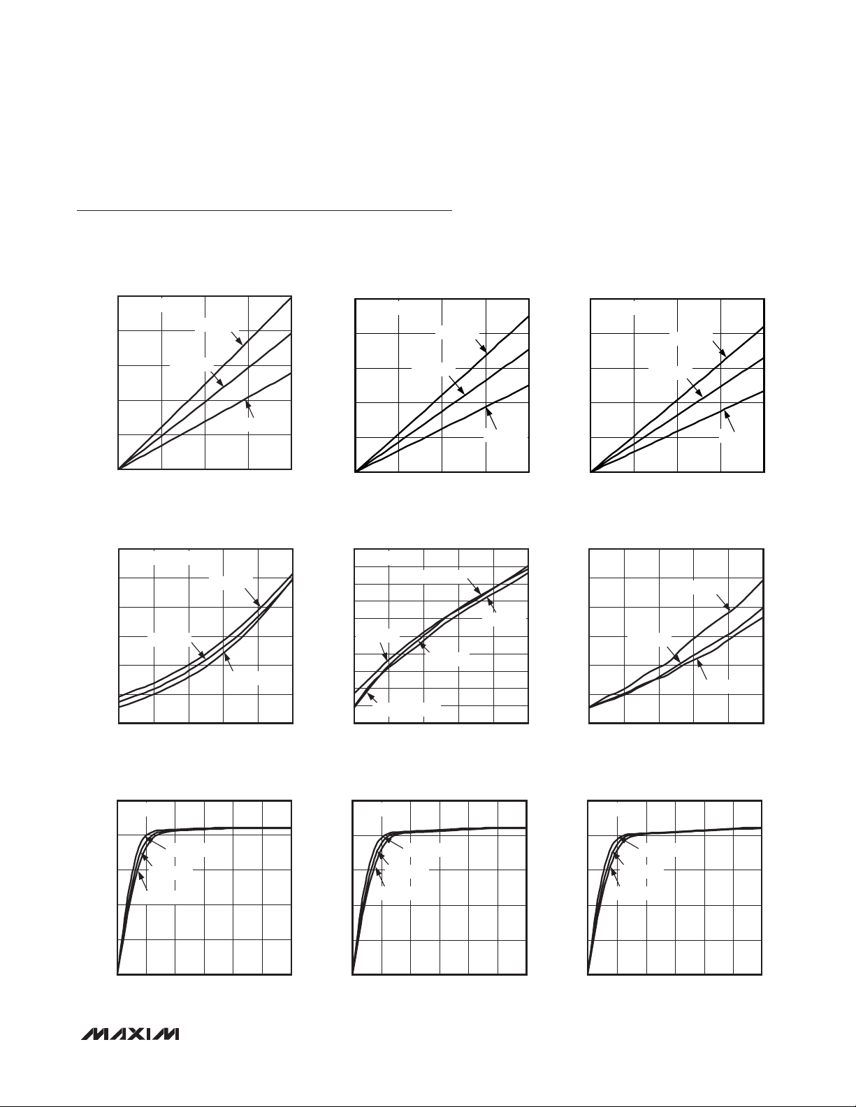
Typical Operating Characteristics
(VCC = +2.5V, TA = +25NC, unless otherwise noted.)
MAX7360
GPO OUTPUT LOW VOLTAGE
vs. SINK CURRENT (COL2–COL7)
250
VCC = 2.4V
200
150
100
OUTPUT VOLTAGE (mV)
50
0
0 20
TA = +85NC
TA = +25NC
SINK CURRENT (mA)
SUPPLY CURRENT
vs. SUPPLY VOLTAGE
45
AUTOSLEEP = OFF
40
35
30
25
SUPPLY CURRENT (A)
20
15
TA = +25NC
2.0
1.6 3.6
SUPPLY VOLTAGE (V)
TA = +85NC
TA = -40NC
2.4
2.8
TA = -40NC
15105
3.2
GPO OUTPUT LOW VOLTAGE
vs. SINK CURRENT (COL2–COL7)
250
VCC = 3.0V
MAX7360 toc01
200
150
100
OUTPUT VOLTAGE (mV)
50
0
0 20
KEY-SWITCH SOURCE CURRENT
18.4
V
= O
COL0
18.3
MAX7360 toc04
18.2
18.1
18.0
TA = +85NC
17.9
17.8
17.7
17.6
KEY-SWITCH SOURCE CURRENT (A)
17.5
TA = -40NC, +25NC
17.4
1.6 3.63.2
TA = +85°C
TA = +25°C
vs. SUPPLY VOLTAGE
TA = -40NC, +85NC
TA = -40NC
2.42.0
2.8
SUPPLY VOLTAGE (V)
TA = -40°C
15105
TA = +25NC
GPO OUTPUT LOW VOLTAGE
vs. SINK CURRENT (COL2–COL7)
250
VCC = 3.6V
MAX7360 toc02
200
150
100
OUTPUT VOLTAGE (mV)
50
0
0 20
SHUTDOWN SUPPLY CURRENT
3.0
2.5
MAX7360 toc05
2.0
1.5
1.0
SHUTDOWN SUPPLY CURRENT (A)
0.5
0
1.6 3.63.2
TA = +85°C
TA = +25°C
vs. SUPPLY VOLTAGE
TA = -40NC
TA = +25NC
TA = +85NC
2.8
2.42.0
SUPPLY VOLTAGE (V)
MAX7360 toc03
TA = -40°C
15105
MAX7360 toc06
SINK CURRENT vs. OUTPUT VOLTAGE
25
VCC = 2.4V
20
TA = -40NC
15
10
SINK CURRENT (mA)
5
0
TA = +25NC
TA = +85NC
0 3.02.5
OUTPUT VOLTAGE (V)
_______________________________________________________________________________________ 5
SINK CURRENT vs. OUTPUT VOLTAGE
25
VCC = 3.0V
MAX7360 toc07
20
TA = -40NC
15
10
SINK CURRENT (mA)
5
0
1.5 2.01.00.5
TA = +25NC
TA = +85NC
0 3.02.5
1.5 2.01.00.5
OUTPUT VOLTAGE (V)
MAX7360 toc08
SINK CURRENT vs. OUTPUT VOLTAGE
25
VCC = 3.6V
20
TA = -40NC
15
10
SINK CURRENT (mA)
5
0
TA = +25NC
TA = +85NC
0 3.02.5
1.5 2.01.00.5
OUTPUT VOLTAGE (V)
MAX7360 toc09
Page 6

I2C-Interfaced Key-Switch Controller and LED
Driver/GPIOs with Integrated ESD Protection
Pin Description
PIN
TQFN WLP
1 A6 ROW0 Row Input from Key Matrix. Leave ROW0 unconnected or connect to GND if unused.
2 B6 ROW1 Row Input from Key Matrix. Leave ROW1 unconnected or connect to GND if unused.
3 C4 ROW2 Row Input from Key Matrix. Leave ROW2 unconnected or connect to GND if unused.
MAX7360
4 C6 ROW3 Row Input from Key Matrix. Leave ROW3 unconnected or connect to GND if unused.
5, 15, 25, 35B4, C5, D2,
E4
6 D6 ROW4 Row Input from Key Matrix. Leave ROW4 unconnected or connect to GND if unused.
7 D5 ROW5 Row Input from Key Matrix. Leave ROW5 unconnected or connect to GND if unused.
8 E6 ROW6 Row Input from Key Matrix. Leave ROW6 unconnected or connect to GND if unused.
9 D4 ROW7 Row Input from Key Matrix. Leave ROW7 unconnected or connect to GND if unused.
10, 20, 27,
30, 40
11 F6 COL0 Column Output to Key Matrix. Leave COL0 unconnected if unused.
12 E5 COL1 Column Output to Key Matrix. Leave COL1 unconnected if unused.
13 F5 COL2
14 F4 COL3
16 F3 COL4
17 E3 COL5
18 F2 COL6
19 F1 COL7
21 E2 SDA I2C-Compatible, Serial-Data I/O
22 E1 SCL I2C-Compatible, Serial-Clock Input
23 D3 INTK
C2 N.C. No Connection. Not internally connected. Leave unconnected.
NAME FUNCTION
GND Ground
Column Output to Key Matrix. Leave COL2 unconnected if unused. COL2 can be
configured as a GPO (see Table 9 in the Register Tables section).
Column Output to Key Matrix. Leave COL3 unconnected if unused. COL3 can be
configured as a GPO (see Table 9 in the Register Tables section).
Column Output to Key Matrix. Leave COL4 unconnected if unused. COL4 can be
configured as a GPO (see Table 9 in the Register Tables section).
Column Output to Key Matrix. Leave COL5 unconnected if unused. COL5 can be
configured as a GPO (see Table 9 in the Register Tables section).
Column Output to Key Matrix. Leave COL6 unconnected if unused. COL6 can be
configured as a GPO (see Table 9 in the Register Tables section).
Column Output to Key Matrix. Leave COL7 unconnected if unused. COL7 can be
configured as a GPO (see Table 9 in the Register Tables section).
Active-Low Key-Switch Interrupt Output. INTK is open drain and requires a pullup
resistor.
6 ______________________________________________________________________________________
Page 7

I2C-Interfaced Key-Switch Controller and LED
Driver/GPIOs with Integrated ESD Protection
Pin Description (continued)
MAX7360
PIN
TQFN WLP
24 D1 INTI Active-Low GPI Interrupt Output. INTI is open drain and requires a pullup resistor.
26 C1 V
28 B1 AD0 Address Input. AD0 selects up to four device slave addresses (Table 3).
29 A1 I.C. Internally Connected. Connect to GND for normal operation.
31 B2 PORT0
32 A2 PORT1
33 B3 PORT2
34 A3 PORT3
36 A4 PORT4
37 C3 PORT5
38 A5 PORT6
39 B5 PORT7
— — EP
NAME FUNCTION
Positive Supply Voltage. Bypass VCC to GND with a 0.1FF or higher ceramic capacitor.
CC
GPIO Port. Open-drain I/O rated at +14V. PORT0 can be configured as a constantcurrent output.
GPIO Port. Open-drain I/O rated at +14V. PORT1 can be configured as a constantcurrent output.
GPIO Port. Open-drain I/O rated at +14V. PORT2 can be configured as a constantcurrent output.
GPIO Port. Open-drain I/O rated at +14V. PORT3 can be configured as a constantcurrent output.
GPIO Port. Open-drain I/O rated at +14V. PORT4 can be configured as a constantcurrent output.
GPIO Port. Open-drain I/O rated at +14V. PORT5 can be configured as a constantcurrent output.
GPIO Port. Open-drain I/O rated at +14V. PORT6 Can be configured as a constantcurrent output, or a rotary switch input.
GPIO Port. Open-drain I/O rated at +14V. PORT7 can be configured as a constantcurrent output, or a rotary switch input.
Exposed Pad (TQFN only). EP is internally connected to GND. Connect EP to a ground
plane to increase thermal performance.
_______________________________________________________________________________________ 7
Page 8
I2C-Interfaced Key-Switch Controller and LED
Driver/GPIOs with Integrated ESD Protection
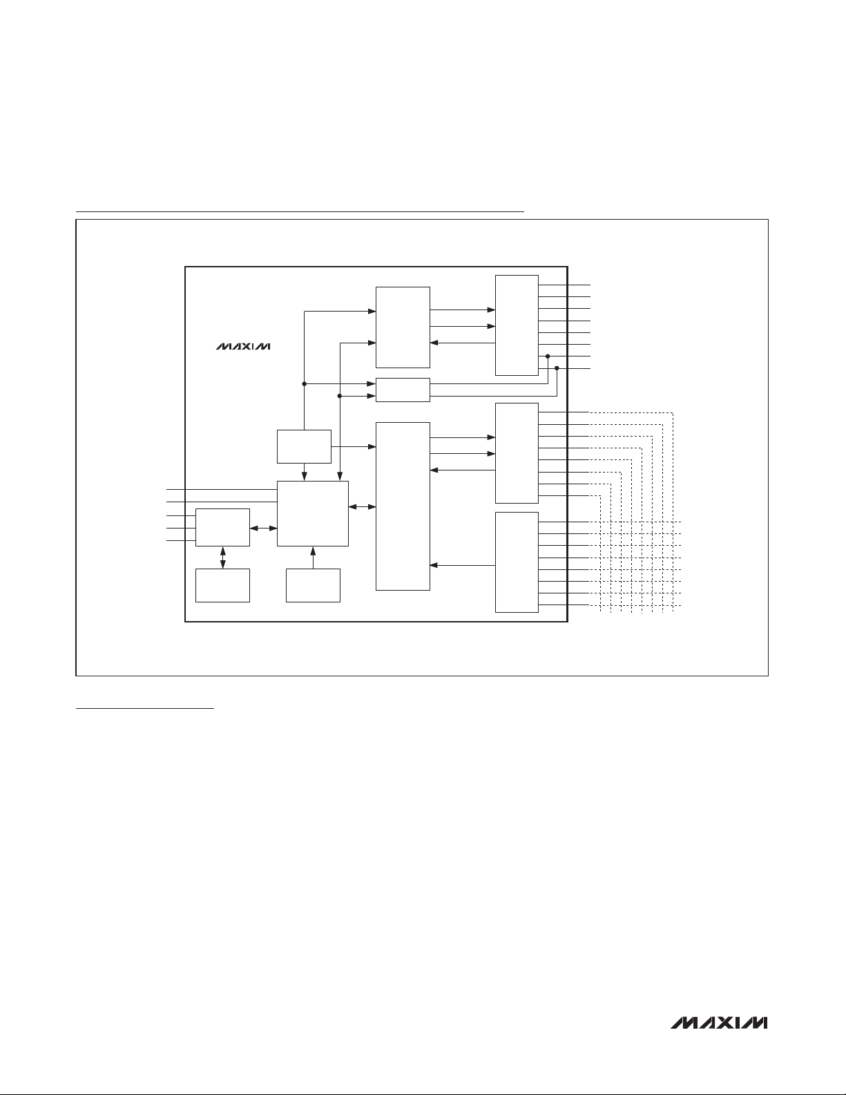
Functional Block Diagram
PORT0
PORT1
PORT2
PORT3
PORT4
PORT5
PORT6
PORT7
COL0
COL1
COL2*
COL3*
COL4*
COL5*
COL6*
COL7*
ROW0
ROW1
ROW2
ROW3
ROW4
ROW5
ROW6
ROW7
MAX7360
INTI
INTK
SDA
SCL
AD0
MAX7360
I2C
INTERFACE
BUS
TIMEOUT
128kHz
OSCILLATOR
CONTROL
REGISTERS
FIFO
POR
PWM
GPIO
LOGIC
ROTARY
KEY
SCAN
LED ENABLE
GPIO ENABLE
GPIO INPUT
COLUMN ENABLE
GPO ENABLE
CURRENT DETECT
ROW ENABLE
PORT GPIO
AND
CONSTANT-
CURRENT
LED DRIVE
CURRENT
SOURCE
COLUMN
DRIVES
OPENDRAIN
ROW
DRIVES
*GPO
Detailed Description
The MAX7360 is a microprocessor peripheral low-noise
key-switch controller that monitors up to 64 key switches
with optional autorepeat, and key events that are
presented in a 16-byte FIFO. The MAX7360 also features
eight open-drain GPIOs configured for digital I/O or
constant-current output for LED applications up to +14V.
The MAX7360 features an automatic sleep mode and
automatic wakeup that further reduce supply current
consumption. The MAX7360 can be configured to enter
sleep mode after a programmable time following a key
event. The FIFO content is maintained and can be read
in sleep mode. The MAX7360 does not enter autosleep
when a key is held down. The autowake feature takes
To prevent overloading the microprocessor with too
many interrupts, interrupt requests are issued on a
programmable number of FIFO entries, and/or after a
set period of time (Table 10). The key-switch status is
checked by reading the key-switch FIFO. A 1-byte read
access returns both the next key event in the FIFO (if
there is one) and the FIFO status. INTK functions as an
open-drain general-purpose output (GPO) capable of
driving an LED if key-switch interrupts are not required.
Up to six of the key-switch outputs function as opendrain GPOs capable of driving additional LEDs when
the application requires fewer keys to be scanned. For
each key-switch output used as a GPO, the number of
monitored key switches reduces by eight.
the MAX7360 out of sleep mode following a keypress
event. Enable/disable autosleep and autowake through
the configuration register (Table 8).
8 ______________________________________________________________________________________
On power-up, all control registers are set to power-up
values and the MAX7360 is in sleep mode (Table 1).
Initial Power-Up
Page 9

I2C-Interfaced Key-Switch Controller and LED
Driver/GPIOs with Integrated ESD Protection
Table 1. Register Address Map and Power-Up Condition
MAX7360
ADDRESS
CODE
(hex)
0x00 Read only 0x3F Keys FIFO Read FIFO key-scan data out
0x01
0x02
0x03
0x04
0x05
0x06
0x40
0x41
0x42
0x43
0x44
0x45
0x46
0x48 Read only 0x00
0x49 Read only 0xFF GPIO input register PORT0–PORT7 input values
0x4A Read only 0x00 Rotary switch count Switch cycles since last read
0x50
0x51
0x52
0x53
0x54
0x55
0x56
0x57
0x58
0x59
0x5A
0x5B
0x5C
0x5D
0x5E
0x5F
READ/
WRITE
R/W
R/W
R/W
R/W
R/W
R/W
R/W
R/W
R/W
R/W
R/W
R/W
R/W
R/W
R/W
R/W
R/W
R/W
R/W
R/W
R/W
R/W
R/W
R/W
R/W
R/W
R/W
R/W
R/W
POWER-UP
VALUE (hex)
0x0A Configuration
0xFF Debounce Key debounce time settling and GPO enable
0x00 Interrupt
0xFE GPO
0x00 Key repeat Delay and frequency for key repeat
0x07 Sleep Idle time to autosleep
0x00
0x00 GPIO control PORT0–PORT7 input/output control
0x00 GPIO debounce PORT0–PORT7 debounce time setting
0xC0
0x00 GPIO output mode PORT0–PORT7 output mode control
0x00 Common PWM Common PWM duty-cycle setting
0x00
0x00 PORT0 PWM PORT0 individual duty-cycle setting
0x00 PORT1 PWM PORT1 individual duty-cycle setting
0x00 PORT2 PWM PORT2 individual duty-cycle setting
0x00 PORT3 PWM PORT3 individual duty-cycle setting
0x00 PORT4 PWM PORT4 individual duty-cycle setting
0x00 PORT5 PWM PORT5 individual duty-cycle setting
0x00 PORT6 PWM PORT6 individual duty-cycle setting
0x00 PORT7 PWM PORT7 individual duty-cycle setting
0x00 PORT0 configuration PORT0 interrupt, PWM mode control and blink period setting
0x00 PORT1 configuration PORT1 interrupt, PWM mode control and blink period setting
0x00 PORT2 configuration PORT2 interrupt, PWM mode control and blink period setting
0x00 PORT3 configuration PORT3 interrupt, PWM mode control and blink period setting
0x00 PORT4 configuration PORT4 interrupt, PWM mode control and blink period setting
0x00 PORT5 configuration PORT5 interrupt, PWM mode control and blink period setting
0x00 PORT6 configuration PORT6 interrupt, PWM mode control and blink period setting
0x00 PORT7 configuration PORT7 interrupt, PWM mode control and blink period setting
REGISTER
FUNCTION
Power-down, key-release enable, autowakeup, and I2C timeout enable
Key-switch interrupt INTK frequency setting
COL2–COL7 and INTK GPO control
GPIO global con-
figuration
GPIO constant-
current setting
Rotary switch con-
figuration
I2C timeout flag I2C timeout since last POR
Rotary switch, GPIO standby, GPIO reset, fade
PORT0–PORT7 constant-current output setting
Rotary switch interrupt frequency and debounce time setting
DESCRIPTION
_______________________________________________________________________________________ 9
Page 10

I2C-Interfaced Key-Switch Controller and LED
Driver/GPIOs with Integrated ESD Protection
Table 2. Key-Switch Mapping
PIN COL0 COL1 COL2* COL3* COL4* COL5* COL6* COL7*
ROW0
ROW1
ROW2
ROW3
ROW4
MAX7360
ROW5
ROW6
ROW7
*These columns can be configured as GPOs.
KEY 0 KEY 8 KEY 16 KEY 24 KEY 32 KEY 40 KEY 48 KEY 56
KEY 1 KEY 9 KEY 17 KEY 25 KEY 33 KEY 41 KEY 49 KEY 57
KEY 2 KEY 10 KEY 18 KEY 26 KEY 34 KEY 42 KEY 50 KEY 58
KEY 3 KEY 11 KEY 19 KEY 27 KEY 35 KEY 43 KEY 51 KEY 59
KEY 4 KEY 12 KEY 20 KEY 28 KEY 36 KEY 44 KEY 52 KEY 60
KEY 5 KEY 13 KEY 21 KEY 29 KEY 37 KEY 45 KEY 53 KEY 61
KEY 6 KEY 14 KEY 22 KEY 30 KEY 38 KEY 46 KEY 54 KEY 62
KEY 7 KEY 15 KEY 23 KEY 31 KEY 39 KEY 47 KEY 55 KEY 63
Key-Scan Controller
Key inputs are scanned statically, not dynamically,
to ensure low-EMI operation. As inputs only toggle
in response to switch changes, the key matrix can be
routed closer to sensitive circuit nodes.
The key-scan controller debounces and maintains a FIFO
of keypress and release events (including autorepeated
keypresses, if autorepeat is enabled). Table 2 shows the
key-switch order. The user-programmable key-switch
debounce time, and autosleep timer, is derived from the
64kHz clock, which in turn is derived from the 128kHz
oscillator. Time delay for autorepeat and key-switch
interrupt is based on the key-switch debounce time.
Keys FIFO Register (0x00)
The keys FIFO register contains the information pertaining
to the status of the keys FIFO, as well as the key events
that have been debounced (see Table 7 in the Register
Tables section). Bits D0–D5 denote which of the 64 keys
have been debounced and the keys are numbered as in
Table 1.
D7 indicates if there is more data in the FIFO, except
when D5:D0 indicate key 63 or key 62. When D5:D0
indicate key 63 or key 62, the host should read one more
time to determine whether there is more data in the FIFO.
Use key 62 and key 63 for rarely used keys. D6 indicates
if it is a keypress or release event, except when D5:D0
indicate key 63 or key 62.
Reading the key-scan FIFO clears the interrupt INTK
depending on the setting of bit D5 in the configuration
register (0x01).
Configuration Register (0x01)
The configuration register controls the I2C bus timeout
feature, enables key-release detection, enables autowake,
and determines how INTK is deasserted. Write to bit D7
to put the MAX7360 into sleep mode or operating mode.
Autosleep and autowake, when enabled, also change the
status of D7 (see Table 8 in the Register Tables section).
Debounce Register (0x02)
The debounce register sets the time for each debounce
cycle, as well as setting whether the GPO ports are
enabled or disabled. Bits D0–D4 set the debounce time
in increments of 1ms starting at 9ms and ending at 40ms
(see Table 9 in the Register Tables section). Bits D5, D6,
and D7 set which of the GPO ports is enabled. Note the
GPO ports are enabled only in the combinations shown
in Table 9, from all disabled to all enabled.
Key-Switch Interrupt Register (0x03)
The interrupt register contains information related to the
settings of the interrupt request function, as well as the
status of the INTK output, which can also be configured
as a GPO. If bits D0–D7 are set to 0x00, the INTK output
is configured as a GPO that is controlled by bit D1 in the
port register. There are two types of interrupts, the FIFObased interrupt and time-based interrupt. Set bits D0–D4
to assert interrupts at the end of the selected number of
debounce cycles following a key event (see Table 10 in
the Register Tables section). This number ranges from
1–31 debounce cycles. Setting bits D7, D6, and D5 set
the FIFO-based interrupt when there are 4–16 key events
stored in the FIFO. Both interrupts can be configured
simultaneously and INTK asserts depending on which
condition is met first. INTK deasserts depending on the
status of bit D5 in the configuration register.
Ports Register (0x04)
The ports register sets the values of PORT2–PORT7
and the INTK port, when configured, as open-drain
10 _____________________________________________________________________________________
Page 11

I2C-Interfaced Key-Switch Controller and LED
Driver/GPIOs with Integrated ESD Protection
GPOs. The settings in this register are ignored for ports
not configured as GPOs, and a read from this register
returns the values stored in the register (see Table 11 in
the Register Tables section).
Autorepeat Register (0x05)
The MAX7360 autorepeat feature notifies the host that at
least one key has been pressed for a continuous period.
The autorepeat register enables or disables this feature,
sets the time delay after the last key event before the key
repeat code (0x7E) is entered into the FIFO, and sets
the frequency at which the key-repeat code is entered
into the FIFO thereafter. Bit D7 specifies whether the
autorepeat function is enabled with 0 denoting autorepeat
disabled, and 1 denoting autorepeat enabled. Bits D0–
D3 specify the autorepeat delay in terms of debounce
cycles ranging from 8–128 debounce cycles (see Table
12 in the Register Tables section). Bits D4, D5, and D6
specify the autorepeat rate or frequency ranging from
4–32 debounce cycles.
When autorepeat is enabled, holding the key pressed
results in a key-repeat event that is denoted by 0x7E. The
key being pressed does not show up again in the FIFO.
Only one autorepeat code is entered into the FIFO,
regardless of the number of keys pressed. The
autorepeat code continues to be entered in the FIFO at
the frequency set by bits D4–D1 until another key event
is recorded. Following the key-release event, if any keys
are still pressed, the MAX7360 restarts the autorepeat
sequence.
Autosleep Register (0x06)
Autosleep puts the MAX7360 in sleep mode to draw
minimal current. When enabled, the MAX7360 enters
sleep mode if no keys are pressed for the autosleep time
(see Table 13 in the Register Tables section).
Key-Switch Sleep Mode
In sleep mode, the MAX7360 draws minimal current.
Switch-matrix current sources are turned off and pulled
up to VCC. When autosleep is enabled, key-switch
inactivity for a period longer than the autosleep time
puts the part into sleep mode (FIFO data is maintained).
Writing a 1 to D7, or a keypress, can take the MAX7360
out of sleep mode. Bit D7 in the configuration register
gives the sleep-mode status and can be read any time.
The FIFO data is maintained while in sleep mode.
Keypresses initiate autowake and the MAX7360 goes into
operating mode. Keypresses that autowake the MAX7360
are not lost. When a key is pressed while the MAX7360
is in sleep mode, all analog circuitry, including switchmatrix current sources, turn on in 2ms. The initial key
needs to be pressed for 2ms plus the debounce time to
be stored in the FIFO. Write a 0 to D1 in the configuration
register (0x01) to disable autowakeup.
The MAX7360 has eight GPIO ports with LED control
functions. The ports can be used as logic inputs, logic
outputs, or constant-current PWM LED drivers. In
addition, PORT7 and PORT8 can function as a rotary
switch input pair. When in PWM mode, the ports are set
up to start their PWM cycle in 45N phase increments. This
prevents large current spikes on the LED supply voltage
when driving multiple LEDs.
GPIO Global Configuration Register (0x40)
The GPIO global configuration register controls the main
settings for the eight GPIOs (see Table 14 in the Register
Tables section).
Bit D7 enables PORT[7:6] as inputs for a rotary switch.
Bit D5 enables interrupt generation for I2C timeouts.
D4 is the main enable/shutdown bit for the GPIOs. D3
functions as a software reset for the GPIO registers (0x40
to 0x5F). Bits D[2:0] set the fade in/out time for the GPIOs
configured as constant-current sinks.
GPIO Control Register (0x41)
The GPIO control register configures each port as either
an input or an output (see Table 15 in the Register Tables
section). All GPIOs allow individual configurations,
and power up as inputs. Enabling rotary switch mode
automatically sets D7 and D6 as inputs. The ports
consume additional current if their inputs are left undriven.
GPIO Debounce Configuration Register (0x42)
The GPIO debounce configuration register sets the
amount of time a GPIO must be held for the MAX7360
to register a logic transition (see Table 16 in the
Register Tables section). The GPIO debounce setting
is independent of the key-switch debounce setting. Five
bits (D[4:0]) set 32 possible debounce times from 9ms
up to 40ms.
Autowake
MAX7360
GPIOs
______________________________________________________________________________________ 11
Page 12

I2C-Interfaced Key-Switch Controller and LED
Driver/GPIOs with Integrated ESD Protection
GPIO Constant-Current Setting Register (0x43)
The GPIO constant-current setting register sets the global
constant-current amount (see Table 17 in the Register
Tables section). Bits D1 and D0 set the global current
values from 5mA up to 20mA.
GPIO Output Mode Register (0x44)
The GPIO output mode register sets an output as either
a constant-current or non-constant-current output for
MAX7360
PORT[7:0] (see Table 18 in the Register Tables section).
Outputs are configured as constant-current outputs by
default to prevent accidental loading of an LED across
an unregulated output. The constant-current circuits
automatically turn off when not in use to reduce current
consumption.
Common PWM Register (0x45)
The common PWM register stores the common constantcurrent output PWM duty cycle (see Table 19 in the
Register Tables section). The values stored in this register
translate over to a PWM duty cycle in the same manner
as the individual PWM registers (0x50 to 0x57). Ports can
use their own individual PWM value, or the common PWM
value. Write to this register to change the duty cycle of
several ports at once.
Rotary Switch Configuration Register (0x46)
The rotary switch configuration register stores rotary
switch settings for PORT7 and PORT6 (see Table 20 in
the Register Tables section). D7 determines whether
switch counts or a time delay will trigger an interrupt
if enabled. D[6:4] set the count or time amount to wait
before sending an interrupt. Bits D[3:0] set the debounce
cycle time for the rotary switch inputs. Debounce time
ranges from 0 to 15ms.
I2C Timeout Flag Register (0x48) (Read Only)
The I2C timeout flag register contains a single bit (D0),
which indicates if an I2C timeout has occurred (see Table
21 in the Register Tables section). Read this register to
clear an I2C timeout initiated interrupt.
GPIO Input Register (0x49) (Read Only)
The GPIO input register contains the input data for all of
the GPIOs (see Table 22 in the Register Tables section).
Ports configured as outputs are read as high. There is
one debounce period delay prior to detecting a transition
on the input port. This prevents a false interrupt from
occurring when changing a port from an output to an
input. The GPIO input register reports the state of all
input ports regardless of any interrupt mask settings.
Ports configured as an input have a 2FA internal pullup
to VCC for PORT[5:0] and a 10FA internal pullup to VCC
for PORT[7:6].
Rotary Switch Count Register (0x4A) (Read Only)
The MAX7360 keeps a count of the rotary switch rotations
in two’s compliment format (see Table 23 in the Register
Tables section). The register values wrap around as the
count value switches from a positive to a negative value
and back again. The count resets to zero after an I2C
read to this register.
PORT0–PORT7 Individual PWM Ratio Registers
(0x50 to 0x57)
Each port has an individual PWM ratio register (0x50 to
0x57, see Table 24 in the Register Tables section). Use
values 0x00 to 0xFE in these registers to configure the
number of cycles out of 256 the output sinks current
(LED is on), from 0 cycles to 254 cycles. Use 0xFF to
have an output continuously sink current (always on).
For applications requiring multiple ports to have the
same intensity, program a particular port’s configuration
register (0x58 to 0x5F) to use the common PWM register
(0x45). New PWM settings take place at the beginning of
a PWM cycle, to allow changes from common intensity to
individual intensity with no interruption in the PWM cycle
PORT0–PORT7 Configuration Registers
(0x58 to 0x5F)
Registers 0x58 to 0x5F set individual configurations for
each port (see Table 25 in the Register Tables section).
Bits D7 and D6 determine the interrupt settings for the
inputs. Interrupts can assert upon detection of a logic
transition, a rising edge, or not at all. D5 sets the port’s
PWM setting to either the common or individual PWM
setting. Bits D[4:2] enable and set the ports’ individual
blink period from 0 to 4096ms. Bits D1 and D0 set a port’s
blink duty cycle.
Fading
Set the fade cycle time in the GPIO global configuration
register (0x40) to a non-zero value to enable fade in/out (see
Table 14 in the Register Tables section). Fade in increases
an LED’s PWM intensity in 16 even steps from zero to its
stored value. Fade out decreases an LED’s PWM intensity in
16 even steps from its current value to zero. Fading occurs
automatically in any of the following scenarios:
1) Change the common PWM register value from any
value to zero to cause all ports using the common
PWM register settings to fade out. No ports using
individual PWM settings are affected.
2) Change the common PWM register value to any value
from zero to cause all ports using the common PWM
register settings to fade in. No ports using individual
PWM settings are affected.
3) Put the part out of shutdown to cause all ports to
fade in. Changing an individual PWM intensity during
12 _____________________________________________________________________________________
Page 13

I2C-Interfaced Key-Switch Controller and LED
Driver/GPIOs with Integrated ESD Protection
fade in automatically cancels that port’s fade and
immediately output at its newly programmed intensity.
4) Put the part into shutdown to cause all ports to fade
out. Changing an individual PWM intensity during
fade out automatically cancels that port’s fade and
immediately turns off.
Blink
Each port has its own blink control settings through
registers 0x58 to 0x5F (see Table 25 in the Register Tables
section). The blink period ranges from 0 (blink disabled)
to 4.096s. Settable blink duty cycles range from 6.25%
to 50%. All blink periods start at the same PWM cycle for
synchronized blinking between multiple ports.
GPIO Port Interrupts (INTI)
Three possible sources generate INTI: I2C timeout,
GPIOs configured as inputs, and the rotary switch
(registers 0x48, 0x49, and 0x4A). Read the respective
data/status registers for each type of interrupt to clear
INTI. Set register 0x46 for rotary switch-based interrupts.
PORT7
PORT6
PORT7
PORT6
ROTARY SWITCH
DEBOUNCE
Figure 1. Rotary Switch Input Signal Timing
INCREMENT
DECREMENT
Set registers 0x58 to 0x5F for individual GPI-based
interrupts. If multiple sources generate the interrupt, all
the related status registers must be read to clear INTI.
Rotary Switch
The MAX7360 can accept a 2-bit rotary switch inputs on
PORT6 and PORT7. Rotation of the switch in a clockwise
direction increments the count. Enable rotary switch
mode from the GPIO global configuration register (0x40).
Several settings for PORT6 and PORT7 occur during
rotary switch mode:
1) Each port has a 10FA pullup to VCC.
2) Register 0x46 sets the debounce time.
3) A debounced rising edge on PORT6 while PORT7 is
high decreases the count.
4) A debounced rising edge on PORT6 while PORT7 is
low increases the count.
For more details, see Figure 1.
Serial Interface
Figure 2 shows the 2-wire serial interface timing details.
Serial Addressing
The MAX7360 operates as a slave that sends and
receives data through an I2C-compatible 2-wire interface.
The interface uses a serial-data line (SDA) and a serialclock line (SCL) to achieve bidirectional communication
between master(s) and slave(s). A master (typically a
microcontroller) initiates all data transfers to and from the
MAX7360 and generates the SCL clock that synchronizes
the data transfer.
The MAX7360’s SDA line operates as both an input and
an open-drain output. A pullup resistor, typically 4.7kI,
MAX7360
SDA
t
SU, DAT
t
LOW
t
SCL
t
HD, STA
START
CONDITION
HIGH
t
t
R
F
Figure 2. 2-Wire Serial Interface Timing Details
______________________________________________________________________________________ 13
t
HD, DAT
t
SU, STA
START CONDITION
REPEATED
t
R
t
HD, STA
t
SU, STO
t
F
t
F,TX
STOP
CONDITION
t
BUF
START
CONDITION
Page 14

I2C-Interfaced Key-Switch Controller and LED
Driver/GPIOs with Integrated ESD Protection
is required on SDA. The MAX7360’s SCL line operates
only as an input. A pullup resistor is required on SCL if
there are multiple masters on the 2-wire interface, or if
the master in a single-master system has an open-drain
SCL output.
Each transmission consists of a START condition (Figure
3) sent by a master, followed by the MAX7360 7-bit slave
address plus R/W bit, a register address byte, one or
MAX7360
more data bytes, and finally, a STOP condition.
START and STOP Conditions
Both SCL and SDA remain high when the interface is not
busy. A master signals the beginning of a transmission
with a START (S) condition by transitioning SDA from
high to low while SCL is high. When the master has
finished communicating with the slave, it issues a STOP
(P) condition by transitioning SDA from low to high while
SCL is high. The bus is then free for another transmission.
Bit Transfer
One data bit is transferred during each clock pulse
(Figure 4). The data on SDA must remain stable while
SCL is high.
Acknowledge
The acknowledge bit is a clocked 9th bit (Figure 4), which
the recipient uses to handshake receipt of each byte of
data. Thus, each byte transferred effectively requires
9 bits. The master generates the 9th clock pulse, and
the recipient pulls down SDA during the acknowledge
clock pulse; therefore, the SDA line is stable low during
the high period of the clock pulse. When the master is
transmitting to the MAX7360, the MAX7360 generates the
acknowledge bit because the MAX7360 is the recipient.
When the MAX7360 is transmitting to the master, the
master generates the acknowledge bit because the
master is the recipient.
Table 3. 2-Wire Interface Address Map
PIN AD0
GND 0 1 1 1 0 0 0
V
CC
SDA 0 1 1 1 1 0 0
SCL 0 1 1 1 1 1 0
A7 A6 A5 A4 A3 A2 A1 A0
0 1 1 1 0 1 0
DEVICE ADDRESS
R/W
R/W
R/W
R/W
SDA
SCL
Figure 3. START and STOP Conditions
Figure 4. Bit Transfer
14 _____________________________________________________________________________________
SDA
SCL
S
START
CONDITION
DATA LINE STABLE;
DATA VALID
CHANGE OF DATA
ALLOWED
P
STOP
CONDITION
Page 15

I2C-Interfaced Key-Switch Controller and LED
Driver/GPIOs with Integrated ESD Protection
Figure 5. Acknowledge
SCL
SDA
TRANSMITTER
SDA
RECEIVER
BY
BY
START
CONDITION
S
1 2 8 9
CLOCK PULSE FOR
ACKNOWLEDGE
MAX7360
SDA
SCL
0 1 1 A3 A2 A11
MSB
LSB
Figure 6. Slave Address
COMMAND BYTE IS STORED ON RECEIPT OF
S A A P0SLAVE ADDRESS COMMAND BYTE
ACKNOWLEDGE CONDITION
ACKNOWLEDGE FROM MAX7360
R/W
D7 D6 D5 D4 D3 D2 D1 D0
ACKNOWLEDGE FROM MAX7360
Figure 7. Command Byte Received
ACKNOWLEDGE FROM MAX7360
D7 D6 D5 D4 D3 D2 D1 D0 D1 D0D3 D2D5 D4D7 D6
ACKNOWLEDGE FROM MAX7360
S A A A P0SLAVE ADDRESS COMMAND BYTE DATA BYTE
R/W
Figure 8. Command and Single Data Byte Received
Slave Addresses
The MAX7360 has a 7-bit long slave address (Figure
6). The bit following a 7-bit slave address is the R/W bit,
which is low for a write command and high for a read
command.
The first 4 bits (MSBs) of the MAX7360 slave address
dynamic signals, care must be taken to ensure that AD0
transitions no sooner than the signals on SDA and SCL.
The MAX7360 monitors the bus continuously, waiting for a
START condition, followed by its slave address. When the
MAX7360 recognizes its slave address, it acknowledges
and is then ready for continued communication.
are always 0111. Slave address bits A3, A2, and A1
correspond, by the matrix in Table 3, to the states of the
device address input AD0, and A0 corresponds to the
R/W bit. The AD0 input can be connected to any of four
signals (GND, VCC, SDA, or SCL), giving four possible
slave address pairs and allowing up to four MAX7360
devices to share the bus. Because SDA and SCL are
The MAX7360 features a 20ms minimum bus timeout
on the 2-wire serial interface, largely to prevent the
MAX7360 from holding the SDA I/O low during a read
transaction should the SCL lock up for any reason before
a serial transaction is completed. Bus timeout operates
by causing the MAX7360 to internally terminate a serial
ACKR/W
ACKNOWLEDGE FROM MAX7360
1 BYTE
AUTOINCREMENT
COMMAND BYTE ADDRESS
Bus Timeout
______________________________________________________________________________________ 15
Page 16

I2C-Interfaced Key-Switch Controller and LED
Driver/GPIOs with Integrated ESD Protection
D7 D6 D5 D4 D3 D2 D1 D0 D1 D0D3 D2D5 D4D7 D6
ACKNOWLEDGE FROM MAX7360
S A A A P0SLAVE ADDRESS COMMAND BYTE DATA BYTE
R/W
MAX7360
Figure 9. N Data Bytes Received
Table 4. Autoincrement Rules
REGISTER
FUNCTION
Keys FIFO 0x00 0x00
Autoshutdown 0x06 0x00
All other key switch 0x01 to 0x05 Addr + 0x01
All other GPIO 0x40 to 0x5F Addr + 0x01
transaction, either read or write, if SCL low exceeds
20ms. After a bus timeout, the MAX7360 waits for a valid
START condition before responding to a consecutive
transmission. This feature can be enabled or disabled
under user control by writing to the configuration register
(Table 8 in the Register Tables section).
A write to the MAX7360 comprises the transmission of the
slave address with the R/W bit set to zero, followed by at
least 1 byte of information. The first byte of information
is the command byte. The command byte determines
which register of the MAX7360 is to be written by the next
byte, if received. If a STOP condition is detected after the
command byte is received, the MAX7360 takes no further
action (Figure 7) beyond storing the command byte.
Any bytes received after the command byte are data bytes.
The first data byte goes into the internal register of the
MAX7360 selected by the command byte (Figure 8).
If multiple data bytes are transmitted before a STOP condition
is detected, these bytes are generally stored in subsequent
MAX7360 internal registers, because the command byte
address generally autoincrements (Table 4).
The MAX7360 is read using the internally stored
command byte as an address pointer, the same way the
stored command byte is used as an address pointer for
a write. The pointer generally autoincrements after each
data byte is read using the same rules as for a write
ADDRESS
CODE (hex)
AUTOINCREMENT
ADDRESS (hex)
Message Format for Writing
the Key-Scan Controller
Message Format for Reading
the Key-Scan Controller
ACKNOWLEDGE FROM MAX7360
(Table 4). Thus, a read is initiated by first configuring the
MAX7360’s command byte by performing a write (Figure
6). The master can now read n consecutive bytes from
the MAX7360, with the first data byte being read from
the register addressed by the initialized command byte.
When performing read-after-write verification, remember
to reset the command byte’s address, because the stored
command byte address is generally autoincremented
after the write (Figure 9, Table 4).
When the MAX7360 is operated on a 2-wire interface with
multiple masters, a master reading the MAX7360 uses a
repeated start between the write that sets the MAX7360’s
address pointer, and the read(s) that takes the data
from the location(s). This is because it is possible for
master 2 to take over the bus after master 1 has set up
the MAX7360’s address pointer, but before master 1
has read the data. If master 2 subsequently resets the
MAX7360’s address pointer, master 1’s read can be from
an unexpected location.
Address autoincrementing allows the MAX7360 to be
configured with fewer transmissions by minimizing the
number of times the command address needs to be sent.
The command address stored in the MAX7360 generally
increments after each data byte is written or read (Table
4). Autoincrement only works when doing a multiburst
read or write.
Applications Information
After a catastrophic event such as ESD discharge or
microcontroller reset, use bit D7 of the configuration
register (0x01) as a software reset for the key-switch
state (the key-switch register values and FIFO remain
unaffected). Use bit D4 of the GPIO global configuration
register (0x40) as a software reset for the GPIOs.
ACKNOWLEDGE FROM MAX7360
N BYTES
AUTOINCREMENT
COMMAND BYTE ADDRESS
Operation with Multiple Masters
Command Address Autoincrementing
Reset from I2C
16 _____________________________________________________________________________________
Page 17

I2C-Interfaced Key-Switch Controller and LED
Driver/GPIOs with Integrated ESD Protection
REGULAR KEYPRESS
EVENT
GHOST-KEY
EVENT
EXAMPLES OF VALID THREE-KEY COMBINATIONS
MAX7360
KEY-SWITCH MATRIX
Figure 10. Ghost-Key Phenomenon
Ghost-Key Elimination
Ghost keys are a phenomenon inherent with key-switch
matrices. When three switches located at the corners
of a matrix rectangle are pressed simultaneously, the
switch that is located at the last corner of the rectangle
(the ghost key) also appears to be pressed. This occurs
because the potentials at the two sides of the ghost-key
switch are identical due to the other three connections—
the switch is electrically shorted by the combination of
the other three switches (Figure 10). Because the key
appears to be pressed electrically, it is impossible to
detect which of the four keys is the ghost key.
The MAX7360 employs a proprietary scheme that detects
any three-key combination that generates a fourth ghost
key, and does not report the third key that causes a
ghost-key event. This means that although ghost keys
are never reported, many combinations of three keys
are effectively ignored when pressed at the same time.
Applications requiring three-key combinations (such
as <Ctrl><Alt><Del>) must ensure that the three keys
are not wired in positions that define the vertices of a
rectangle (Figure 11). There is no limit on the number of
keys that can be pressed simultaneously as long as the
keys do not generate ghost-key events and FIFO is not full.
Low-EMI Operation
The MAX7360 uses two techniques to minimize EMI
radiating from the key-switch wiring. First, the voltage
across the switch matrix never exceeds +0.55V if not in
sleep mode, independent of supply voltage VCC. This
reduces the voltage swing at any node when a switch
is pressed to +0.55V maximum. Second, the keys are
not dynamically scanned, which would cause the keyswitch wiring to continuously radiate interference.
Instead, the keys are monitored for current draw (only
occurs when pressed), and debounce circuitry only
operates when one or more keys are actually pressed.
KEY-SWITCH MATRIX KEY-SWITCH MATRIX
Figure 11. Valid Three-Key Combinations
Switch On-Resistance
The MAX7360 is designed to be insensitive to resistance,
either in the key switches, or the switch routing to and
from the appropriate COL_ and ROW_ up to 4kI (max).
These controllers are therefore compatible with low-cost
membrane and conductive carbon switches.
Hot Insertion
The INTI, INTK, SCL, and AD0 inputs and SDA remain
high impedance with up to +3.6V asserted on them when
the MAX7360 powers down (VCC = 0). I/O ports (PORT0–
PORT7) remain high impedance with up to +14V asserted
on them when not powered. Use the MAX7360 in hot-
swap applications.
Staggered PWM
The LED’s on-time in each PWM cycle are phase
delayed 45N into eight evenly spaced start positions.
Optimize phasing when using fewer than eight ports as
constant-current outputs by allocating the ports with the
most appropriate start positions. For example, if using
four constant-current outputs, choose PORT0, PORT2,
PORT4, and PORT6 because their PWM start positions
are evenly spaced. In general, choose the ports that
spread the PWM start positions as evenly as possible.
This optimally spreads out the current demand from the
ports’ load supply.
INTK/INTI
There are two interrupt outputs, INTK and INTI. Each
interrupt operates independently from the other. See
the Key-Switch Interrupt Register (0x03) and the GPIO
Port Interrupts (INTI) sections for additional information
regarding these two interrupts.
Power-Supply Considerations
The MAX7360 operates with a +1.62V to +3.6V power-
supply voltage. Bypass the power supply to GND with a
0.1FF or higher ceramic capacitor as close as possible
to the device.
______________________________________________________________________________________ 17
Page 18

I2C-Interfaced Key-Switch Controller and LED
Driver/GPIOs with Integrated ESD Protection
ESD Protection
All of the MAX7360 pins meet the 2kV Human Body Model
ESD tolerances. Key-switch inputs and GPIOs meet IEC
61000-4-2 ESD protection. The IEC test stresses consist
of 10 consecutive ESD discharges per polarity, at the
maximum specified level and below (per IEC 61000-4-2).
Test criteria include:
1) The powered device does not latch up during the
MAX7360
ESD discharge event.
2) The device subsequently passes the final test used
for prescreening.
Tables 5 and 6 are from the IEC 61000-4-2: Edition 1.1
1999-05: Electromagnetic compatibility (EMC) Testing
and measurement techniques—Electrostatic discharge
immunity test
Table 6. ESD Waveform Parameters
INDICATED
LEVEL
1 2 7.5 0.7 to 1 4 2
2 4 15 0.7 to 1 8 4
3 6 22.5 0.7 to 1 12 6
4 8 30 0.7 to 1 16 8
VOLTGE
(kV)
FIRST PEAK OF
CURRENT
DISCHARGE ±10%
(A)
Table 5. ESD Test Levels
1A—CONTACT
DISCHARGE
LEVEL
1 2 1 2
2 4 2 4
3 6 3 8
4 8 4 10
X Special X Special
X = Open level. The level has to be specified in the
dedicated equipment specification. If higher voltages
than those shown are specified, special test equipment
could be needed.
RISE TIME (tr) WITH
DISCHARGE SWITCH
(ns)
TEST
VOLTAGE (kV)
CURRENT (±30%)
AT 30ns
(A)
1B—AIR-GAP DISCHARGE
LEVEL
TEST
VOLTAGE (kV)
CURRENT
(±30%) AT 60ns
(A)
18 _____________________________________________________________________________________
Page 19

I2C-Interfaced Key-Switch Controller and LED
Driver/GPIOs with Integrated ESD Protection
Register Tables
Table 7. Keys FIFO Register Format (0x00)
MAX7360
SPECIAL FUNCTION
The key number indicated by D5:D0 is a key
event. D7 is always for a key press of key 62
and key 63. When D7 is 0, the key read is the
last data in the FIFO. When D7 is 1, there is
more data in the FIFO. When D6 is 1, key data
read from FIFO is a key release. When D6 is 0,
key data read from FIFO is a key press.
FIFO is empty. 0 0 1 1 1 1 1 1
FIFO is overflow. Continue to read data in FIFO. 0 1 1 1 1 1 1 1
Key 63 is pressed. Read one more time to
determine whether there is more data in FIFO.
Key 63 is released. Read one more time to
determine whether there is more data in FIFO.
Key repeat. Indicates the last data in FIFO. 0 0 1 1 1 1 1 0
Key repeat. Indicates more data in FIFO. 0 1 1 1 1 1 1 0
Key 62 is pressed. Read one more time to
determine whether there is more data in FIFO.
Key 62 is released. Read one more time to
determine whether there is more data in FIFO.
D7 D6 D5 D4 D3 D2 D1 D0
FIFO
empty
flag
1 0 1 1 1 1 1 1
1 1 1 1 1 1 1 1
1 0 1 1 1 1 1 0
1 1 1 1 1 1 1 0
Key
release
flag
KEYS FIFO REGISTER DATA
X X X X X X
______________________________________________________________________________________ 19
Page 20

I2C-Interfaced Key-Switch Controller and LED
Driver/GPIOs with Integrated ESD Protection
Table 8. Configuration Register Format (0x01)
REGISTER
BIT
MAX7360
D7 Sleep
D6 Reserved 0 — 0
D5 Interrupt
D4 Reserved 0 — 0
D3
D2 Reserved 0 — 0
D1
D0
DESCRIPTION VALUE FUNCTION
Key-release
enable
Autowakeup
enable
Timeout
disable
X
(when 0x40
D4 = 1)
0
(when 0x40
D4 = 0)
1
(when 0x40
D4 = 0)
0
1
0 Disable key releases
1 Enable key releases
0 Disable keypress wakeup
1 Enable keypress wakeup
0
1
Key-switch operating mode. Key switches always remain active
when constant-current PWM is enabled (bit 4 of register 0x40 is
high) regardless of autosleep, autowakeup, or an I2C write to this bit.
Key-switch sleep
mode. The entire
chip is shut down.
Key-switch operating
mode
INTK cleared when FIFO is empty
INTK cleared after host read. In this mode, I2C should read the
FIFO until interrupt condition is removed or further INT may be lost.
I2C timeout enabled
I2C timeout disabled
When constant-current PWM is disabled
(bit 4 of register 0x40 is low), I2C write,
autosleep, and autowakeup all can change
this bit. This bit can be read back by I2C
any time for current status.
DEFAULT
VALUE
0
0
1
1
0
Table 9. Debounce Register Format (0x02)
REGISTER DATA
REGISTER DESCRIPTION
Debounce time is 9ms X X X 0 0 0 0 0
Debounce time is 10ms X X X 0 0 0 0 1
Debounce time is 11ms X X X 0 0 0 1 0
Debounce time is 12ms X X X 0 0 0 1 1
Debounce time is 37ms X X X 1 1 1 0 0
Debounce time is 38ms X X X 1 1 1 0 1
Debounce time is 39ms X X X 1 1 1 1 0
Debounce time is 40ms X X X 1 1 1 1 1
GPO ports disabled (full key-scan functionality) 0 0 0 X X X X X
GPO port 7 enabled 0 0 1 X X X X X
GPO ports 7 and 6 enabled 0 1 0 X X X X X
20 _____________________________________________________________________________________
D7 D6 D5 D4 D3 D2 D1 D0
PORTS ENABLE DEBOUNCE TIME
.
.
.
Page 21

I2C-Interfaced Key-Switch Controller and LED
Driver/GPIOs with Integrated ESD Protection
Table 9. Debounce Register Format (0x02) (continued)
REGISTER DATA
REGISTER DESCRIPTION
GPO ports 7, 6, and 5 enabled 0 1 1 X X X X X
GPO ports 7, 6, 5, and 4 enabled 1 0 0 X X X X X
GPO ports 7, 6, 5, 4, and 3 enabled 1 0 1 X X X X X
GPO ports 7, 6, 5, 4, 3, and 2 enabled 1 1 X X X X X X
Power-up default setting 1 1 1 1 1 1 1 1
Table 10. Key-Switch Interrupt Register Format (0x03)
REGISTER DESCRIPTION
INTK used as GPO
FIFO-based INTK disabled
INTK asserts every debounce cycle
INTK asserts every 2 debounce cycles
D7 D6 D5 D4 D3 D2 D1 D0
PORTS ENABLE DEBOUNCE TIME
REGISTER DATA
D7 D6 D5 D4 D3 D2 D1 D0
FIFO-BASED INTK TIME-BASED INTK
0 0 0 0 0 0 0 0
0 0 0 Not all zero
0 0 0 0 0 0 0 1
0 0 0 0 0 0 1 0
MAX7360
.
.
.
INTK asserts every 29 debounce cycles
INTK asserts every 30 debounce cycles
INTK asserts every 31 debounce cycles
Time-based INTK disabled
INTK asserts when FIFO has 2 key events
INTK asserts when FIFO has 4 key events
INTK asserts when FIFO has 6 key events
INTK asserts when FIFO has 16 key events
Both time-based and FIFO-based interrupts
active
Power-up default setting 0 0 0 0 0 0 0 0
0 0 0 1 1 1 0 1
0 0 0 1 1 1 1 0
0 0 0 1 1 1 1 1
Not all zero 0 0 0 0 0
0 0 1 0 0 0 0 0
0 1 0 0 0 0 0 0
0 1 1 0 0 0 0 0
.
.
.
1 1 1 0 0 0 0 0
Not all zero Not all zero
______________________________________________________________________________________ 21
Page 22

I2C-Interfaced Key-Switch Controller and LED
Driver/GPIOs with Integrated ESD Protection
Table 11. Ports Register Format (0x04)
REGISTER
BIT
D7 PORT 7 Control
D6 PORT 6 Control
MAX7360
D5 PORT 5 Control
D4 PORT 4 Control
D3 PORT 3 Control
D2 PORT 2 Control
D1
D0 Reserved 0 — 0
DESCRIPTION VALUE FUNCTION
0 Clear port 7 low
1 Set port 7 high (high impedance)
0 Clear port 6 low
1 Set port 6 high (high impedance)
0 Clear port 5 low
1 Set port 5 high (high impedance)
0 Clear port 4 low
1 Set port 4 high (high impedance)
0 Clear port 3 low
1 Set port 3 high (high impedance)
0 Clear port 2 low
1 Set port 2 high (high impedance)
INTK Port
Control
0
1
Clear port INTK low
Set port INTK high (high impedance)
DEFAULT
VALUE
1
1
1
1
1
1
1
22 _____________________________________________________________________________________
Page 23

I2C-Interfaced Key-Switch Controller and LED
Driver/GPIOs with Integrated ESD Protection
Table 12. Autorepeat Register Format (0x05)
REGISTER DATA
REGISTER DESCRIPTION
Autorepeat is disabled 0 X X X X X X X
Autorepeat is enabled 1
D7 D6 D5 D4 D3 D2 D1 D0
ENABLE AUTOREPEAT RATE AUTOREPEAT DELAY
AUTOREPEAT RATE AUTOREPEAT DELAY
MAX7360
Key-switch autorepeat delay is 8 debounce
cycles
Key-switch autorepeat delay is 16 debounce
cycles
Key-switch autorepeat delay is 24 debounce
cycles
Key-switch autorepeat delay is 112 debounce
cycles
Key-switch autorepeat delay is 120 debounce
cycles
Key-switch autorepeat delay is 128 debounce
cycles
Key-switch autorepeat frequency is 4
debounce cycles
Key-switch autorepeat frequency is 8
debounce cycles
Key-switch autorepeat frequency is 12
debounce cycles
1 X X X 0 0 0 0
1 X X X 0 0 0 1
1 X X X 0 0 1 0
.
.
.
1 X X X 1 1 0 1
1 X X X 1 1 1 0
1 X X X 1 1 1 1
1 0 0 0 X X X X
1 0 0 1 X X X X
1 0 1 0 X X X X
.
.
.
Key-switch autorepeat frequency is 32
debounce cycles
Power-up default setting 0 0 0 0 0 0 0 0
______________________________________________________________________________________ 23
1 1 1 1 X X X X
Page 24

I2C-Interfaced Key-Switch Controller and LED
Driver/GPIOs with Integrated ESD Protection
Table 13. Autosleep Register Format (0x06)
REGISTER REGISTER DATA
AUTOSLEEP REGISTER
No Autosleep 0 0 0 0 0 0 0 0
Autosleep for (ms)
8192 0 0 0 0 0 0 0 1
MAX7360
4096 0 0 0 0 0 0 1 0
2048 0 0 0 0 0 0 1 1
1024 0 0 0 0 0 1 0 0
512 0 0 0 0 0 1 0 1
256 0 0 0 0 0 1 1 0
256 0 0 0 0 0 1 1 1
Power-up default settings 0 0 0 0 0 1 1 1
D7 D6 D5 D4 D3 D2 D1 D0
Table 14. GPIO Global Configuration Register (0x40)
REGISTER
BIT
D7
D6 Reserved 0 — 0
D5
D4 GPIO enable
D3 GPIO reset
D[2:0]
DESCRIPTION VALUE FUNCTION
PORT6/PORT7
rotary switch
I2C timeout
interrupt
enable
Fade in/out
time
0 PORT6/PORT7 operate as GPIOs
1 PORT6/PORT7 operate as a rotary switch input
0 Disabled
1
0
1
0 Normal operation
1
000 No fading
XXX
INTI is asserted when I2C bus times out. INTI is deasserted when a
read is performed on the I2C timeout flag register (0x48).
PWM, constant-current circuits, and GPIs are shut down. GPO
values depend on their setting. Register 0x41 to 0x5F values are
stored and cannot be changed. The entire part is shut down if the
key switches are in sleep mode (D7 of register 0x01).
Normal GPIO operation. PWM, constant-current circuits, and GPIOs are
enabled regardless of key-switch sleep mode state (see Table 8).
Return all GPIO registers (registers 0x40 to 0x5F) to their POR value.
This bit is momentary and resets itself to 0 after the write cycle.
PWM intensity ramps up (down) between the common PWM value
and 0% duty cycle in 16 steps over the following time period:
D[2:0] = 001 = 256ms
D[2:0] = 010 = 512ms
D[2:0] = 011 = 1024ms
D[2:0] = 100 = 2048ms
D[2:0] = 101 = 4096ms
D[2:0] = 110/111 = Undefined
RESERVED AUTOSHUTDOWN TIME
DEFAULT
VALUE
0
0
0
0
000
24 _____________________________________________________________________________________
Page 25

I2C-Interfaced Key-Switch Controller and LED
Driver/GPIOs with Integrated ESD Protection
Table 15. GPIO Control Register (0x41)
REGISTER
BIT
D7 PORT7
D6 PORT6
D5 PORT5
D4 PORT4
D3 PORT3
D2 PORT2
D1 PORT1
D0 PORT0
DESCRIPTION VALUE FUNCTION
0 Port is an input
1 Port is an output
0 Port is an input
1 Port is an output
0 Port is an input
1 Port is an output
0 Port is an input
1 Port is an output
0 Port is an input
1 Port is an output
0 Port is an input
1 Port is an output
0 Port is an input
1 Port is an output
0 Port is an input
1 Port is an output
DEFAULT
MAX7360
VALUE
0
0
0
0
0
0
0
0
Table 16. GPIO Debounce Configuration Register (0x42)
REGISTER DATA
REGISTER DESCRIPTION
Power-up default setting
debounce time is 9ms
Debounce time is 10ms 0 0 0 0 0 0 0 1
Debounce time is 11ms 0 0 0 0 0 0 1 0
Debounce time is 12ms 0 0 0 0 0 0 1 1
Debounce time is 37ms 0 0 0 1 1 1 0 0
Debounce time is 38ms 0 0 0 1 1 1 0 1
Debounce time is 39ms 0 0 0 1 1 1 1 0
Debounce time is 40ms 0 0 0 1 1 1 1 1
D7 D6 D5 D4 D3 D2 D1 D0
RESERVED DEBOUNCE TIME
0 0 0 0 0 0 0 0
.
.
.
______________________________________________________________________________________ 25
Page 26

I2C-Interfaced Key-Switch Controller and LED
Driver/GPIOs with Integrated ESD Protection
Table 17. GPIO Constant-Current Setting Register (0x43)
REGISTER
BIT
D[7:6] Reserved 11 Set always as 11 11
D[5:2] Reserved 0000 — 0000
MAX7360
D[1:0]
DESCRIPTION VALUE FUNCTION
00 Constant current is 5mA
Constant-
current setting
01 Constant current is 6.67mA
10 Constant current is 10mA
11 Constant current is 20mA
Table 18. GPIO Output Mode Register (0x44)
REGISTER
BIT
D7 PORT7
D6 PORT6
D5 PORT5
D4 PORT4
D3 PORT3
D2 PORT2
D1 PORT1
D0 PORT0
DESCRIPTION VALUE FUNCTION
0 Port is a constant-current open-drain output
1 Port is a non-constant-current open-drain output
0 Port is a constant-current open-drain output
1 Port is a non-constant-current open-drain output
0 Port is a constant-current open-drain output
1 Port is a non-constant-current open-drain output
0 Port is a constant-current open-drain output
1 Port is a non-constant-current open-drain output
0 Port is a constant-current open-drain output
1 Port is a non-constant-current open-drain output
0 Port is a constant-current open-drain output
1 Port is a non-constant-current open-drain output
0 Port is a constant-current open-drain output
1 Port is a non-constant-current open-drain output
0 Port is a constant-current open-drain output
1 Port is a non-constant-current open-drain output
DEFAULT
VALUE
00
DEFAULT
VALUE
0
0
0
0
0
0
0
0
Table 19. Common PWM Register (0x45)
REGISTER DATA
REGISTER DESCRIPTION
Power-up default setting (common
PWM ratio is 0/256)
Common PWM ratio is 1/256 0 0 0 0 0 0 0 1
Common PWM ratio is 2/256 0 0 0 0 0 0 1 0
Common PWM ratio is 3/256 0 0 0 0 0 0 1 1
26 _____________________________________________________________________________________
D7 D6 D5 D4 D3 D2 D1 D0
COMMON PWM
0 0 0 0 0 0 0 0
.
.
.
Page 27

I2C-Interfaced Key-Switch Controller and LED
Driver/GPIOs with Integrated ESD Protection
Table 19. Common PWM Register (0x45) (continued)
REGISTER DATA
REGISTER DESCRIPTION
Common PWM ratio is 252/256 1 1 1 1 1 1 0 0
Common PWM ratio is 253/256 1 1 1 1 1 1 0 1
Common PWM ratio is 254/256 1 1 1 1 1 1 1 0
Common PWM ratio is 256/256
(100% duty cycle)
Table 20. Rotary Switch Configuration Register (0x46)
REGISTER DESCRIPTION
No debounce time X X X X 0 0 0 0
Debounce time is 1ms X X X X 0 0 0 1
Debounce time is 2ms X X X X 0 0 1 0
Debounce time is 3ms X X X X 0 0 1 1
Debounce time is 15ms X X X X 1 1 1 1
No interrupt generated by rotary switch X 0 0 0 X X X X
INTI asserted when rotary switch count = ±1
INTI asserted when rotary switch count = ±2
INTI asserted when rotary switch count = ±3
INTI asserted when rotary switch count = ±7
INTI asserted 25ms after first debounced event
INTI asserted 50ms after first debounced event
INTI asserted 75ms after first debounced event
INTI asserted 175ms after first debounced event
Power-up default setting
D7 D6 D5 D4 D3 D2 D1 D0
COMMON PWM
1 1 1 1 1 1 1 1
REGISTER DATA
D7 D6 D5 D4 D3 D2 D1 D0
INT
TYPE
0 0 0 1 X X X X
0 0 1 0 X X X X
0 0 1 1 X X X X
0 1 1 1 X X X X
1 0 0 1 X X X X
1 0 1 0 X X X X
1 0 1 1 X X X X
1 1 1 1 X X X X
0 0 0 0 0 0 0 0
COUNTS/CYCLES DEBOUNCE CYCLE TIME
.
.
.
.
.
.
.
.
.
MAX7360
______________________________________________________________________________________ 27
Page 28

I2C-Interfaced Key-Switch Controller and LED
Driver/GPIOs with Integrated ESD Protection
Table 21. I2C Timeout Flag Register (0x48) (Read Only)
REGISTER
BIT
D[7:1] Reserved 0000000 — 0000000
D0
MAX7360
DESCRIPTION VALUE FUNCTION
I2C timeout flag
0
1
No I2C timeout has occurred since last read or POR
I2C timeout has occurred since last read or POR. This bit is reset to
zero when a read is performed on this register. I2C timeouts must
be enabled for this function to work (see Table 8).
Table 22. GPIO Input Register (0x49) (Read Only)
REGISTER
BIT
D7 PORT7
D6 PORT6
D5 PORT5
D4 PORT4
D3 PORT3
D2 PORT2
D1 PORT1
D0 PORT0
DESCRIPTION VALUE FUNCTION
0 Port is input low
1 Port is input high
0 Port is input low
1 Port is input high
0 Port is input low
1 Port is input high
0 Port is input low
1 Port is input high
0 Port is input low
1 Port is input high
0 Port is input low
1 Port is input high
0 Port is input low
1 Port is input high
0 Port is input low
1 Port is input high
DEFAULT
VALUE
DEFAULT
VALUE
0
0
0
0
0
0
0
0
0
Table 23. Rotary Switch Count Register (0x4A) (Read Only)
REGISTER DATA
REGISTER DESCRIPTION
Cycle count in two’s complement (see the
Rotary Switch Configuration (0x46) section)
28 _____________________________________________________________________________________
D7 D6 D5 D4 D3 D2 D1 D0
CYCLE COUNT
X X X X X X X X
Page 29

I2C-Interfaced Key-Switch Controller and LED
Driver/GPIOs with Integrated ESD Protection
Table 24. PORT0–PORT7 Individual PWM Ratio Registers (0x50 to 0x57)
REGISTER DATA
REGISTER DESCRIPTION
Power-up default setting (port PWM ratio is
0/256)
PORT PWM ratio is 1/256 0 0 0 0 0 0 0 1
PORT PWM ratio is 2/256 0 0 0 0 0 0 1 0
PORT PWM ratio is 3/256 0 0 0 0 0 0 1 1
PORT PWM ratio is 252/256 1 1 1 1 1 1 0 0
PORT PWM ratio is 253/256 1 1 1 1 1 1 0 1
PORT PWM ratio is 254/256 1 1 1 1 1 1 1 0
PORT PWM ratio is 256/256 (100% duty cycle)
Table 25. PORT0–PORT7 Configuration Registers (0x58 to 0x5F)
REGISTER
BIT
D7 Interrupt mask
D6
D5 Common PWM
D[4:2] Blink period
D[1:0] Blink-on time
DESCRIPTION VALUE FUNCTION
0 Interrupt is not masked
1
Edge/level
detect
0
1
0 Port uses individual PWM intensity register to set the PWM ratio
1 Port uses common PWM intensity register to set the PWM ratio
000 Port does not blink
001 Port blink period is 256ms
010 Port blink period is 512ms
011 Port blink period is 1024ms
100 Port blink period is 2048ms
101 Port blink period is 4096ms
110/111 Undefined
00 LED is on for 50% of the blink period
01 LED is on for 25% of the blink period
10 LED is on for 12.5% of the blink period
11 LED is on for 6.25% of the blink period
D7 D6 D5 D4 D3 D2 D1 D0
PORT PWM
0 0 0 0 0 0 0 0
.
.
.
1 1 1 1 1 1 1 1
Interrupt is masked. PORT7 interrupt mask is ignored when the
device is configured for rotary switch input.
Rising edge-triggered
interrupts
Rising or falling edgetriggered interrupts
Interrupts only occur when the GPIO
port is configured as an input
DEFAULT
VALUE
MAX7360
0
0
0
000
00
______________________________________________________________________________________ 29
Page 30

I2C-Interfaced Key-Switch Controller and LED
Driver/GPIOs with Integrated ESD Protection
Pin Configurations
TOP VIEW
MAX7360
BUMPS IN BOTTOM
I.C.
AD0
V
C1
PORT1
A1
B1
A2
PORT0
B2
N.C.
CC
C2
PORT3
A3
PORT2
B3
PORT5
C3
MAX7360
PORT4
A4
GND
B4
ROW2
C4
PORT6
A5
PORT7
B5
GND
C5
ROW0
A6
ROW1
B6
ROW3
C6
TOP VIEW
PORT0
PORT1
PORT2
PORT3
GND
PORT4
PORT5
PORT6
PORT7
N.C.
INTI
D1
SCL
COL7
31
32
33
34
35
36
37
38
39
40
E1
F1
N.C.
+
1 2
GND
SDA
COL6
I.C.
INTK
D2
E2
F2
D3
COL5
E3
COL4
F3
WLP
(2.67mm x 2.67mm)
N.C.
AD0
27282930 26
MAX7360
4 5 6 7
3
CC
V
ROW7
D4
GND
E4
COL3
F4
GND
25
ROW5
D5
COL1
E5
COL2
F5
INTI
INTK
24 23 22
EP*
8 9 10
SCL
ROW4
D6
ROW6
E6
COL0
F6
SDA
21
20
N.C.
19
COL7
COL6
18
17
COL5
16
COL4
GND
15
14
COL3
COL2
13
12
COL1
11
COL0
ROW0
ROW1
ROW2
ROW3
GND
ROW4
ROW5
ROW6
ROW7
N.C.
TQFN
*EP = EXPOSED PAD, CONNECT EP TO GROUND.
30 _____________________________________________________________________________________
Page 31

I2C-Interfaced Key-Switch Controller and LED
Typical Application Circuit
PORT6
PORT7
PORT5
PORT4
PORT3
PORT2
PORT1
PORT0
MAX7360
ROW7
ROW6
ROW5
ROW4
ROW3
ROW2
ROW1
ROW0
SDA
SCL
INTI
INTK
AD0
COL0
COL1
COL2
COL3
COL4
COL5
COL6
COL7
GND
V
CC
SCL
SDA
INTI
INTK
+1.8V
GND
µC
V
CC
+14V
+3.3V
+14V
+3.3V
KEY 0
KEY 1
KEY 2
KEY 3
KEY 4
KEY 5
KEY 6
KEY 7
KEY 8
KEY 9
KEY 10
KEY 11
KEY 12
KEY 13
KEY 14
KEY 15
KEY 16
KEY 17
KEY 18
KEY 19
KEY 20
KEY 21
KEY 22
KEY 23
KEY 24
KEY 25
KEY 26
KEY 27
KEY 28
KEY 29
KEY 30
KEY 31
KEY 32
KEY 33
KEY 34
KEY 35
KEY 36
KEY 37
KEY 38
KEY 39
KEY 40
KEY 41
KEY 42
KEY 43
KEY 44
KEY 45
KEY 46
KEY 47
Driver/GPIOs with Integrated ESD Protection
MAX7360
Chip Information
PROCESS: BiCMOS
Maxim cannot assume responsibility for use of any circuitry other than circuitry entirely embodied in a Maxim product. No circuit patent licenses are implied.
Maxim reserves the right to change the circuitry and specifications without notice at any time.
Maxim Integrated Products, 120 San Gabriel Drive, Sunnyvale, CA 94086 408-737-7600 31
©
2009 Maxim Integrated Products Maxim is a registered trademark of Maxim Integrated Products, Inc.
Package Information
For the latest package outline information and land patterns, go
to www.maxim-ic.com/packages.
PACKAGE TYPE PACKAGE CODE DOCUMENT NO.
40 TQFN-EP T4055+1
36 WLP W362A2+1
21-0140
21-0301
 Loading...