

Page 1
General Description
The MAX7356/MAX7357/MAX7358 8-channel I2C
switches/multiplexers expand the main I
2
C bus to any
combination of 8 extended I
2
C buses. They enable a
master on the main bus to isolate and communicate
with devices or groups of devices that may otherwise
have slave address conflicts. Any extended bus can be
connected or disconnected by control packets from the
main I2C bus writing to the main control register of
these I
2
C switches.
The MAX7357 and MAX7358 feature an enhanced
mode that includes a built-in timer used to monitor all
extended buses for lock-up conditions. If the clock or
data line of any of these buses is low for more than
25ms (typ), a lock condition is detected. An optional
interrupt can be generated through the bidirectional
RST/INT. The master can read the bus lock-up register
to find out which extended bus is locked up. The master can also enable the MAX7357 or the MAX7358 to
send a “flush-out” sequence on the faulty channel.
There is an optional preconnection check that
can be enabled to toggle the extended bus clock and
data line low then high to ensure the downstream bus is
not locked high prior to connecting it to the host bus.
The MAX7356/MAX7357/MAX7358 are transparent
to signals sent and received at each channel, allowing
multiple masters. Any device connected to an I
2
C
bus can transmit and receive signals; however, only the
master connected to the host side of the MAX7356/
MAX7357/MAX7358 should address the device.
The MAX7356/MAX7357/MAX7358 are available in 24-pin
TSSOP and TQFN packages and are specified over the
extended -40°C to +85°C temperature range.
Applications
Features
o Bus Lock-Up Detection and Isolation (MAX7357,
MAX7358)
o Host Notification on Detection of Lock-Up
(MAX7357, MAX7358)
o Maintain Fault Diagnostic Information (MAX7357,
MAX7358)
o Dual-Function RST/INT Provides Lock-Up
Notification and Hardware Reset (MAX7357,
MAX7358)
o RST Input Resets I
2
C Interface (MAX7358)
o 3 Address Control Inputs
o Low RONSwitches
o Logic-Level Translation
o Low 0.1µA (typ) Standby Current
o Support Hot Insertion
o 100kbps Standard-Mode or 400kbps Fast-Mode
I
2
C Interface
o Address Translation Allows Multiple Device with
Same ID
o 5.5V-Tolerant Inputs
o 2.3V to 5.5V Supply
MAX7356/MAX7357/MAX7358
1-to-8 I2C Bus Switches/Multiplexers with Bus
Lock-Up Detection, Isolation, and Notification
________________________________________________________________
Maxim Integrated Products
1
19-4207; Rev 0; 9/08
For pricing, delivery, and ordering information, please contact Maxim Direct at 1-888-629-4642,
or visit Maxim’s website at www.maxim-ic.com.
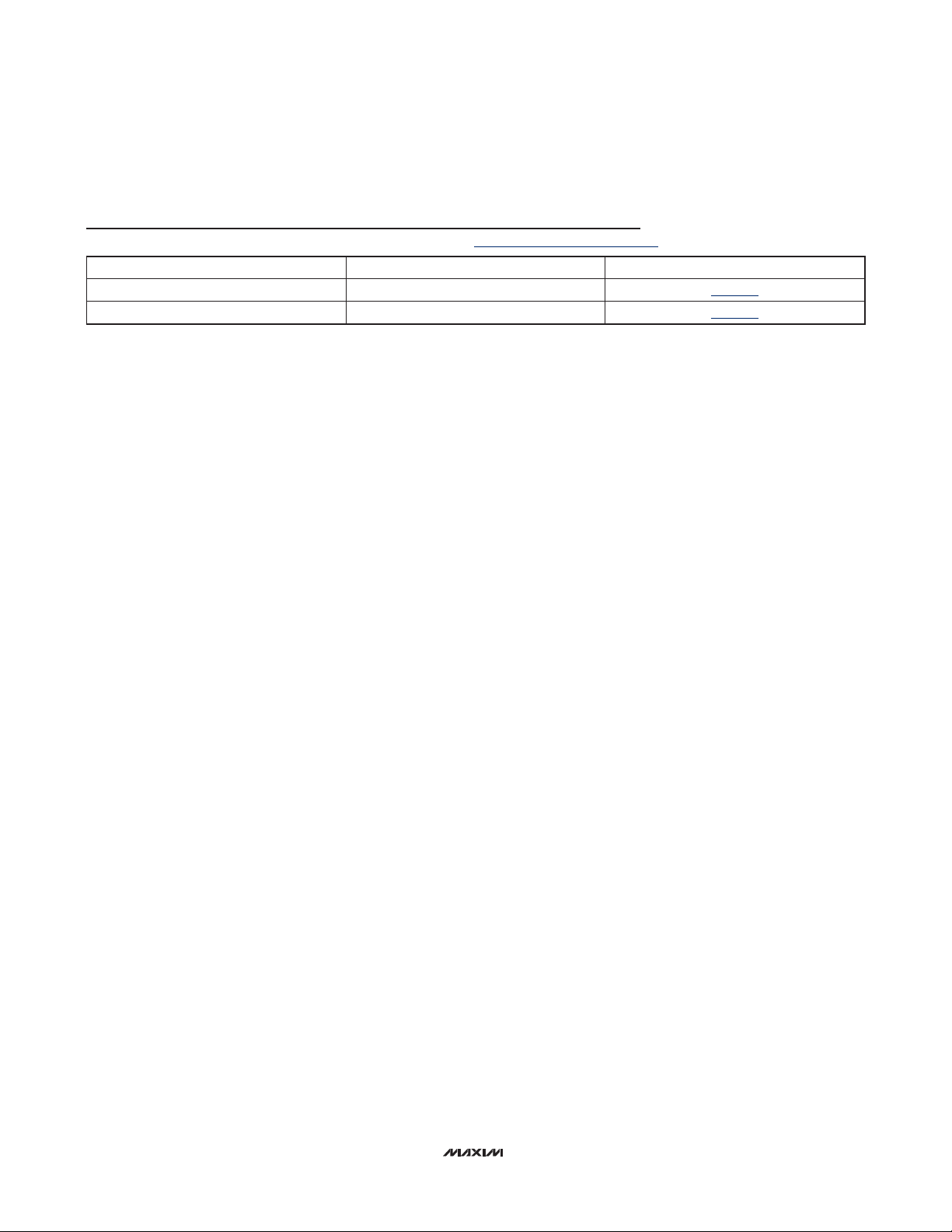
Ordering Information
+
Denotes a lead-free/RoHS-compliant package.
*
EP = Exposed pad.
**
Future product—contact factory for availability.
Typical Operating Circuit and Pin Configurations appear at end of data sheet.
Selector Guide
Servers
RAID
Base Stations
Control and Automation Devices
SFP Control Interface
Networking Equipment
PART TEMP RANGE PIN-PACKAGE
MAX7356ETG+ -40°C to +85°C 24 TQFN-EP*
MAX7356EUG+** -40°C to +85°C 24 TSSOP
MAX7357ETG+ -40°C to +85°C 24 TQFN-EP*
MAX7357EUG+** -40°C to +85°C 24 TSSOP
MAX7358ETG+ -40°C to +85°C 24 TQFN-EP*
MAX7358EUG+** -40°C to +85°C 24 TSSOP
PART
MAX7356 No No Basic mode RST only
MAX7357 Yes Yes, enhanced mode only Enhanced mode Yes
MAX7358 Yes Yes, enhanced mode only Basic mode Yes
ENHANCED
MODE
PRECONNECTION
WIGGLE TEST
POWER-UP
STATE
BIDIRECTIONAL
RST/INT
Page 2
MAX7356/MAX7357/MAX7358
1-to-8 I2C Bus Switches/Multiplexers with Bus
Lock-Up Detection, Isolation, and Notification
2 _______________________________________________________________________________________
ABSOLUTE MAXIMUM RATINGS
ELECTRICAL CHARACTERISTICS (3.3V SUPPLY)
(VDD= +2.3V to +3.6V, TA= -40°C to +85°C, unless otherwise noted. Typical values are at VDD= +3.3V, TA= +25°C.) (Notes 2–5)
Stresses beyond those listed under “Absolute Maximum Ratings” may cause permanent damage to the device. These are stress ratings only, and functional
operation of the device at these or any other conditions beyond those indicated in the operational sections of the specifications is not implied. Exposure to
absolute maximum rating conditions for extended periods may affect device reliability.
Note 1: Package thermal resistances were obtained using the method described in JEDEC specification JESD51-7, using a 4-layer
board. For detailed information on package thermal considerations, refer to www.maxim-ic.com/thermal-tutorial
.
(Voltages referenced to GND.)
VDD.................................................................. -0.3V to +6.0V
All Other Pins.....................................................-0.3V to +6.0V
Input Currents
V
DD
...............................................................................100mA
GND ..............................................................................100mA
All Input Pins.....................................................................±20mA
Output Current ....................................................................25mA
Continuous Power Dissipation (T
A
= +70°C)
24-Pin TSSOP (derate 13.9mW/°C above +70°C) .....1111mW
24-Pin TQFN (derate 27.8mW/°C above +70°C) .......2222mW
Junction-to-Case Thermal Resistance (
θ
JC
) (Note 1)
24-Pin TSSOP...............................................................13°C/W
24-Pin TQFN................................................................3.0°C/W
Junction-to-Ambient Thermal Resistance (
θ
JA
) (Note 1)
24-Pin TSSOP............................................................72.0°C/W
24-Pin TQFN..............................................................36.0°C/W
Operating Temperature Range ......................... -40°C to +85°C
Junction Temperature .................................................... +150°C
Storage Temperature Range ........................... -65°C to +150°C
Lead Temperature (soldering, 10s) ................................+300°C
PARAMETER SYMBOL CONDITIONS MIN TYP MAX UNITS
POWER SUPPLY
Supply Voltage V
Supply Current I
Standby Current I
Power-On Reset Voltage V
Power-On Reset Hysteresis V
INPUT SCL, INPUT/OUTPUT SDA
Low-Level Input Voltage V
High-Level Input Voltage V
Low-Level Output Current I
Input Leakage Current ILH, I
Input Capacitance C
SELECT INPUTS A0 to A2, RST
Low-Level Input Voltage V
High-Level Input Voltage V
Input Leakage Current I
Input Capacitance C
DD
DD
STB
POR
HYST
IL
IH
OL
I
IL
IH
LI
I
VDD = 3.6V;
no load, f
400kHz
No load, VI = V
VDD rising 0.9 1.4 2.1 V
VOL = 0.4V 3
VOL = 0.6V 6
V
LI
and V
SCL
VI = GND 15 pF
A0 to A2, and RST at VDD or GND -1 +1 µA
VI = GND 2 pF
Basic mode 30 50
=
SCL
Enhanced mode
(MAX7357/MAX7358 only)
or GND, VDD = 3.6V 0.1 1 µA
DD
= VDD or GND -1 +1 µA
SDA
2.3 3.6 V
0.7 x
V
DD
0.7 x
V
DD
45 70
0.4 V
0.3 x
V
DD
0.3 x
V
DD
µA
V
V
mA
V
V
Page 3
MAX7356/MAX7357/MAX7358
1-to-8 I2C Bus Switches/Multiplexers with Bus
Lock-Up Detection, Isolation, and Notification
_______________________________________________________________________________________ 3
ELECTRICAL CHARACTERISTICS (3.3V SUPPLY) (continued)
(VDD= +2.3V to +3.6V, TA= -40°C to +85°C, unless otherwise noted. Typical values are at VDD= +3.3V, TA= +25°C.) (Notes 2–5)
ELECTRICAL CHARACTERISTICS (5V SUPPLY)
(VDD= +4.5V to +5.5V, TA= -40°C to +85°C, unless otherwise noted. Typical values are at VDD= +5V, TA= +25°C.) (Notes 2–5)
PASS GATE
Switch Resistance R
Switch Output Voltage V
Leakage Current I
Input/Output Capacitance C
OUTPUT RST/INT
Low-Level Output Current I
Leakage Current ILH, I
PARAMETER SYMBOL CONDITIONS MIN TYP MAX UNITS
ON
SW
VDD = 3.0V to 3.6V, VO = 0.4V, IO = 15mA 5 11 30
VDD = 2.3V to 2.7V, VO = 0.4V, IO = 10mA 7 16 55
V
= VDD = 3.3V, I
SWin
V
= V
S Wi n
V
= VDD = 2.5V, I
SWin
V
= V
S Wi n
= 3.0V to 3.6V , I
D D
= 2.3V to 2.7V , I
D D
= -100µA 1.9
SWout
= - 100µA 1.6 2.8
S Wo ut
= -100µA 1.5
SWout
= - 100µA 1.1 2.0
S Wo ut
Basic mode -1 +1
OL
VI = VDD or GND
L
VI = GND 3 pF
IO
Enhanced mode
(MAX7357/MAX7358)
-2 +2
VOL = 0.4V (MAX7357/MAX7358) 3 mA
V
LI
= VDD or GND -1 +1 µA
RST/INT
µA
POWER SUPPLY
Supply Voltage V
Supply Current I
Standby Current I
Power-On Reset Voltage V
Power-On Reset Hysteresis V
INPUT SCL, INPUT/OUTPUT SDA
Low-Level Input Voltage V
High-Level Input Voltage V
Low-Level Output Current I
Input Leakage Current ILH, I
Input Capacitance C
SELECT INPUTS A0 TO A2, RST
Low-Level Input Voltage V
High-Level Input Voltage V
Input Leakage Current I
PARAMETER SYMBOL CONDITIONS MIN TYP MAX UNITS
DD
DD
STB
POR
HYST
IL
IH
OL
I
IL
IH
LI
VDD = 5V;
no load, f
400kHz
No load, VI = V
Basic mode 65 100
=
Enhanced mode
SCL
(MAX7357/MAX7358 only)
or GND, VDD = 5.5V 0.2 1 µA
DD
VDD rising 0.9 1.4 2.1 V
V
= 0.4V 3
OL
= 0.6V 6
V
OL
V
= V
LI
SCL
= VDD or GND -1 +1 µA
SDA
VI = GND 15 pF
A0 to A2, and RST pins at VDD or GND -1 +1 µA
4.5 5.5 V
90 130
0.4 V
0.3 x
V
DD
0.7 x
V
DD
0.3 x
V
DD
0.7 x
V
DD
µA
mA
Ω
V
V
V
V
V
Page 4
MAX7356/MAX7357/MAX7358
1-to-8 I2C Bus Switches/Multiplexers with Bus
Lock-Up Detection, Isolation, and Notification
4 _______________________________________________________________________________________
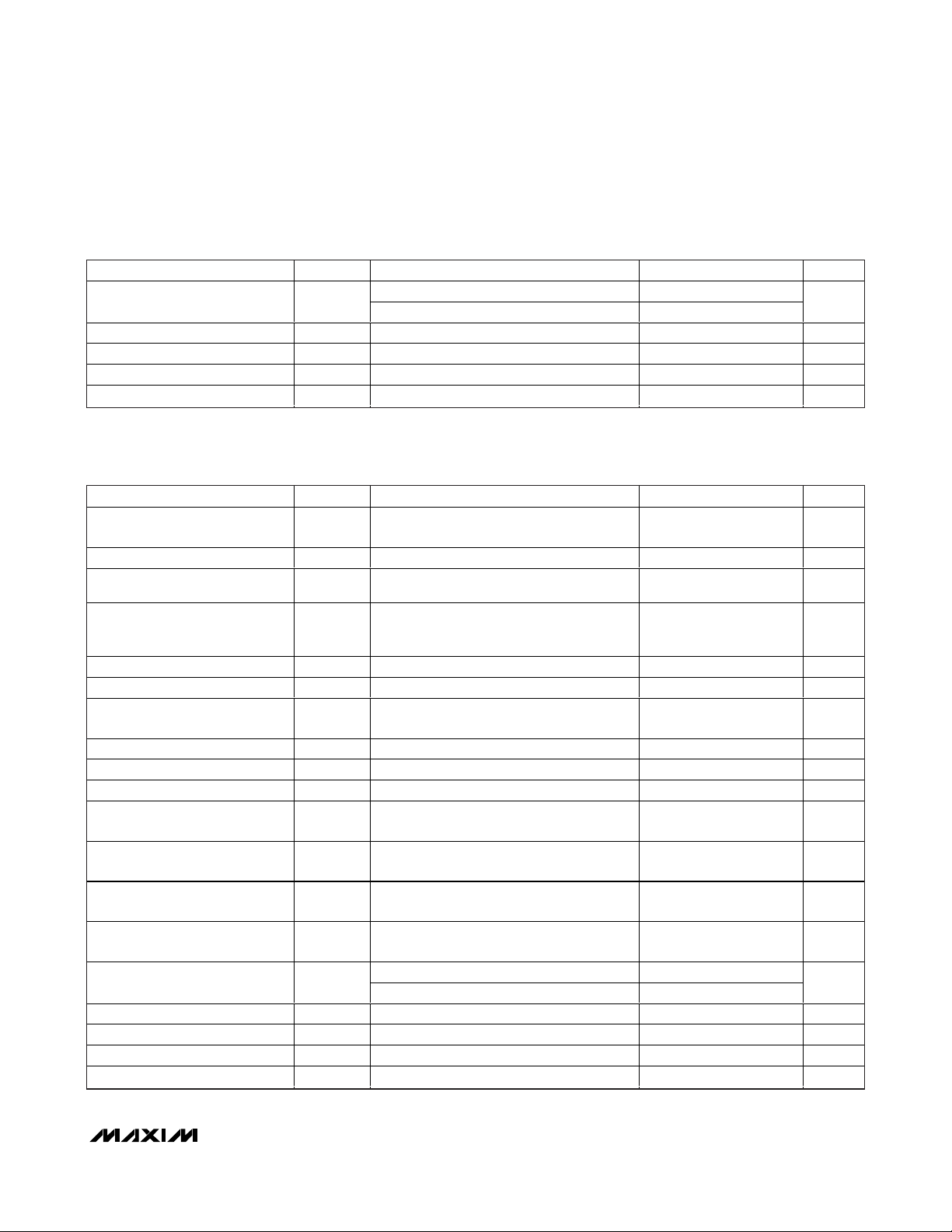
TIMING CHARACTERISTICS (STANDARD-MODE) (Figures 1, 2, 3)
(VDD= 2.3V to 5.5V, TA= -40°C to +85°C, unless otherwise noted.) (Notes 2, 6)
ELECTRICAL CHARACTERISTICS (5V SUPPLY) (continued)
(VDD= +4.5V to +5.5V, TA= -40°C to +85°C, unless otherwise noted. Typical values are at VDD= +5V, TA= +25°C.) (Notes 2–5)
PARAMETER SYMBOL CONDITIONS MIN TYP MAX UNITS
Input Capacitance C
PASS GATE
Switch Resistance R
Switch Output Voltage V
Leakage Current I
Input/Output Capacitance C
OUTPUT RST/INT
Low-Level Output Current I
Leakage Current ILH, I
ON
SW
OL
Propagation Delay from SDA to
SD_ or SCL to SC_
SCL Clock Frequency f
Bus Free Time Between a STOP
and START Condition
Hold Time (Repeated) START
Condition After this Period, the
First Clock Pulse is Generated
LOW Period of the SCL Clock t
HIGH Period of the SCL Clock t
Setup Time for a Repeated
START Condition
Setup Time for a STOP Condition t
Data Hold Time t
Data Setup Time t
Rise Time of Both SDA and SCL
Signals
Fall Time of Both SDA and SCL
Signals
Capacitive Load for Each Bus
Line
Pulse Width of Spikes that Must
be Suppressed by the Input Filter
PARAMETER SYMBOL CONDITIONS MIN TYP MAX UNITS
t
PD
SCL
t
BUF
t
HD;STA
LOW
HIGH
t
SU;STA
SU;STO
HD;DAT
SU;DAT
t
t
C
t
SP
VI = GND 2 pF
I
VDD = 4.5V to 5.5V, VO = 0.4V, IO = 15mA 4 9 24 Ω
V
= VDD = 5.0V, I
SWin
V
= V
S Wi n
VI = VDD or GND
L
VI = GND 3 pF
IO
VOL = 0.4V (MAX7357/MAX7358) 3 mA
V
LI
RST/INT
(Note 7) 0.3 ns
(Note 8) 0 3.45 µs
R
F
b
= 4.5V to 5.5V , I
D D
= VDD or GND -1 +1 µA
= -100µA 3.6
SWout
= - 100µA 2.6 4.5
S Wo ut
MAX7356 -1 +1
Enhanced mode
(MAX7357/MAX7358)
-2 +2
0 100 kHz
4.7 µs
4.0 µs
4.7 µs
4.0 µs
4.7 µs
4.0 µs
250 ns
1000 ns
300 ns
400 pF
50 ns
V
µA
Page 5
MAX7356/MAX7357/MAX7358
1-to-8 I2C Bus Switches/Multiplexers with Bus
Lock-Up Detection, Isolation, and Notification
_______________________________________________________________________________________ 5
TIMING CHARACTERISTICS (STANDARD-MODE) (Figures 1, 2, 3) (continued)
(VDD= 2.3V to 5.5V, TA= -40°C to +85°C, unless otherwise noted.) (Notes 2, 6)
TIMING CHARACTERISTICS (FAST-MODE) (Figures 1, 2, 3)
(VDD= 2.3V to 5.5V, TA= -40°C to +85°C, unless otherwise noted.) (Notes 2, 6)
PARAMETER SYMBOL CONDITIONS MIN TYP MAX UNITS
Data Valid Time t
Data Valid Acknowledge t
Low-Level Reset Time t
Reset Time t
Recovery to Start t
VD;DAT
VD:ACK
REC;STA
WL(rst)
rst
(High to low) 1
(Low to high) 0.6
5ns
500 ns
0ns
PARAMETER SYMBOL CONDITIONS MIN TYP MAX UNITS
Propagation Delay from SDA to
SD_ or SCL to SC_
SCL Clock Frequency f
Bus Free Time Between a STOP
and START Condition
Hold Time (Repeated) START
Condition After this Period,
the Fi r st C l ock P ul se i s Gener ated
LOW Period of the SCL Clock t
HIGH Period of the SCL Clock t
Setup Time for a Repeated
START Condition
Setup Time for a STOP Condition t
Data Hold Time t
Data Setup Time t
Rise Time of Both SDA and SCL
Signals
Fall Time of Both SDA and SCL
Signals
Capacitive Load for Each Bus
Line
Pulse Width of Spikes that Must
be Suppressed by the Input Filter
Data Valid Time t
Data Valid Acknowledge t
Low-Level Reset Time t
Reset Time t
Recovery to START t
t
HD;STA
t
SU;STA
SU;STO
HD;DAT
SU;DAT
VD;DAT
VD;ACK
REC;STA
t
PD
SCL
t
BUF
LOW
HIGH
t
t
C
t
SP
WL(rst)
rst
(Note 7) 0.3 ns
0 400 kHz
1.3 µs
0.6 µs
1.3 µs
0.6 µs
0.6 µs
0.6 µs
(Note 8) 0 0.9 µs
100 ns
R
F
b
(High to low) 1
(Low to high) 0.6
20 +
0.1C
b
20 +
0.1C
b
5ns
500 ns
0ns
µs
1µs
300 ns
300 ns
400 pF
50 ns
µs
1µs
Page 6
MAX7356/MAX7357/MAX7358
1-to-8 I2C Bus Switches/Multiplexers with Bus
Lock-Up Detection, Isolation, and Notification
6 _______________________________________________________________________________________
TIMING CHARACTERISTICS (FAST-MODE) (Figures 1, 2, 3) (continued)
(VDD= 2.3V to 5.5V, TA= -40°C to +85°C, unless otherwise noted.) (Notes 2, 6)
Note 2: All devices are 100% production tested at T
A
= +25°C. Specifications are over -40°C to +85°C and are guaranteed by
design.
Note 3: Subscript SW refers to all SC_ and SD_ pins.
Note 4: V
SWin
= Switch input voltage; I
SWout
= Current between SD_ and SDA or SC_ and SCL. See Figure 4.
Note 5: V
I
= V
SD_
or V
SC_
.
Note 6: All timing is measured using 20% and 80% levels, unless otherwise noted.
Note 7: Pass gate propagation delay is calculated from the 20Ω typical R
ON
and the 15pF load capacitance.
Note 8: A device must internally provide a hold time of at least 300ns for the SDA signal (referred to the V
IH(min)
of the SCL signed)
to bridge the undefined region of the falling edge of SCL.
SDA
SCL
t
BUF
t
SU;STO
t
SP
t
HD;STA
t
SU;STA
t
F
t
HIGH
t
HD;DAT
t
R
t
LOW
t
HD;STA
SP
Sr
P
t
SU;DAT
Figure 1. 2-Wire Serial-Interface Timing Diagram
SCL
SDA
RESET
t
REC;STA
t
WL(rst)
t
rst
Figure 2. RST Timing Diagram
Page 7
MAX7356/MAX7357/MAX7358
1-to-8 I2C Bus Switches/Multiplexers with Bus
Lock-Up Detection, Isolation, and Notification
_______________________________________________________________________________________ 7
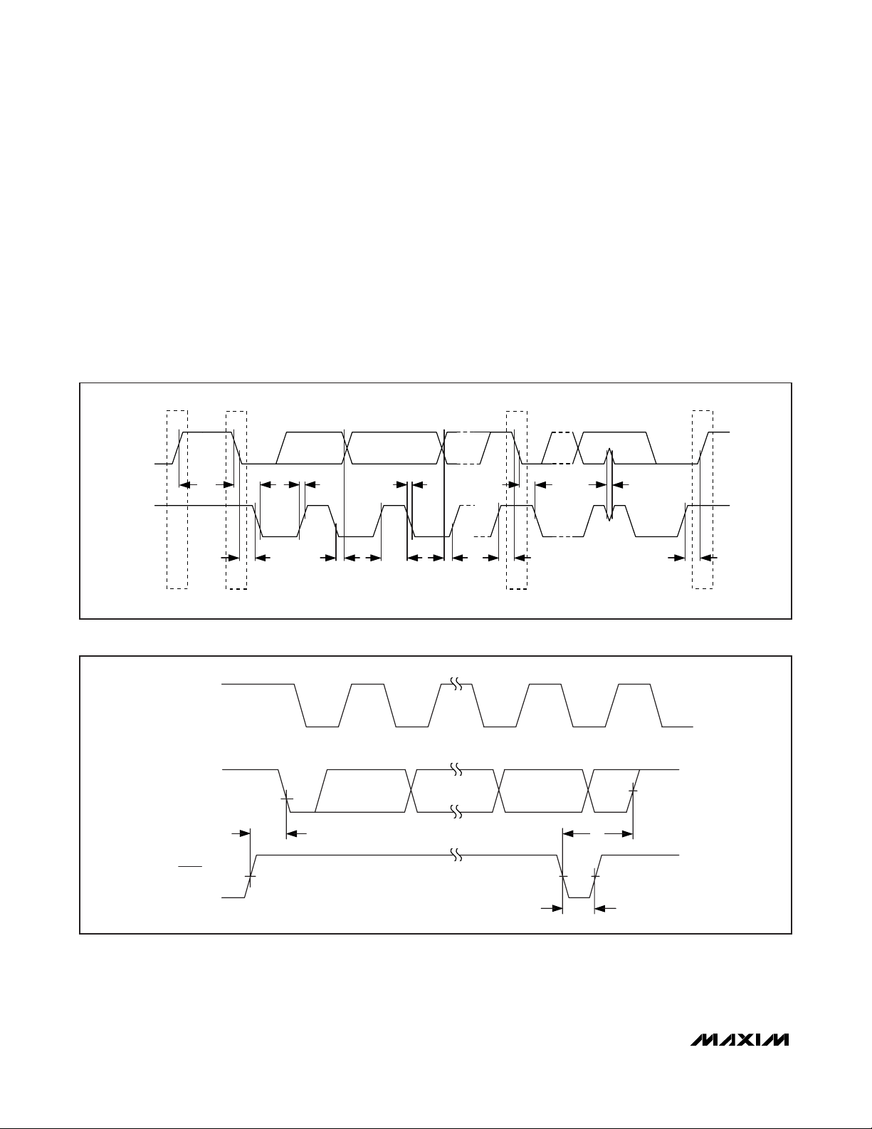
Figure 3. I2C Bus Timing Diagram
Figure 4. Switch Output Voltage and Current
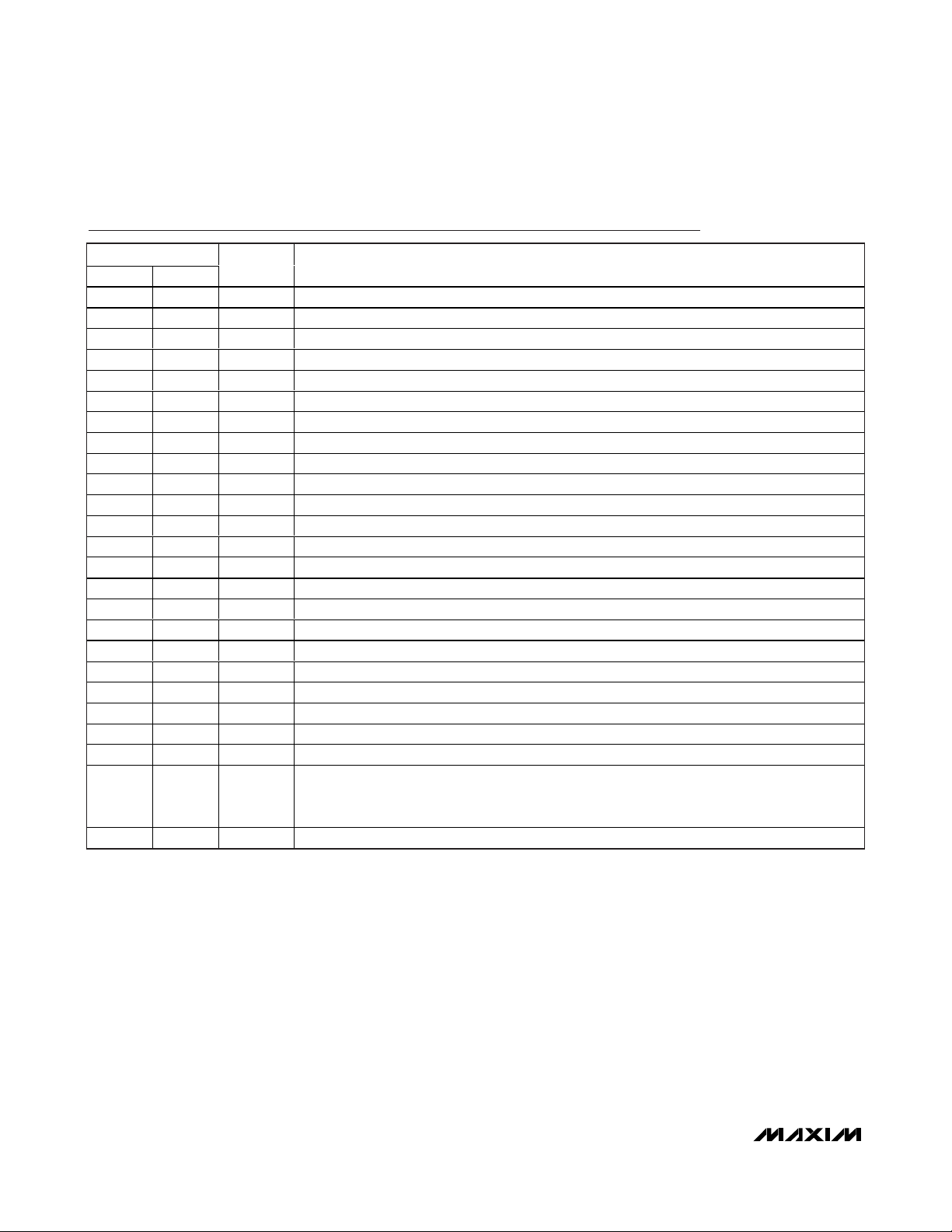
Typical Operating Characteristics
(VDD= +5V, TA= +25°C, unless otherwise noted.)
START
t
SU;STA
CONDITION
(S)
PROTOCOL
SCL
t
BUF
SDA
t
HD;STA
DEVICE
+
V
SWin
-
BIT 7
MSB
(A7)
t
LOWtHIGH
t
r
V
SW
I
SWout
t
VD;ACK
STOP
CONDITION
(P)
t
SU;STO
BIT 6
(A6)
1/f
SCL
t
f
t
SU;DAT
t
HD;DAT
BIT 0
(R/W)
ACKNOWLEDGE
t
VD;DAT
(A)
V
vs. SUPPLY VOLTAGE
SW
I
= 100µA
SWout
2.3 5.5
VDD (V)
4.73.93.1
MAX7356 toc01
(V)
V
5.5
5.0
4.5
4.0
3.5
3.0
SW
2.5
2.0
1.5
1.0
0.5
0
SUPPLY CURRENT vs. SUPPLY VOLTAGE
100
f
= 400kHz
SCL
80
ENHANCED MODE
60
(µA)
DD
I
40
20
0
2.3 5.5
BASIC MODE
VDD (V)
SUPPLY CURRENT vs. SCL FREQUENCY
100
MAX7356 toc02
80
60
(µA)
DD
I
4.73.93.1
ENHANCED MODE
40
f
(kHz)
SCL
BASIC MODE
300200100
20
0
0400
MAX7356 toc03
Page 8
MAX7356/MAX7357/MAX7358
1-to-8 I2C Bus Switches/Multiplexers with Bus
Lock-Up Detection, Isolation, and Notification
8 _______________________________________________________________________________________
Pin Description
( ) For the MAX7357/MAX7358 only.
PIN
TQFN TSSOP
1 4 SD0 I2C Bus0 Serial Data
2 5 SC0 I2C Bus0 Serial Clock
3 6 SD1 I2C Bus1 Serial Data
4 7 SC1 I2C Bus1 Serial Clock
5 8 SD2 I2C Bus2 Serial Data
6 9 SC2 I2C Bus2 Serial Clock
7 10 SD3 I2C Bus3 Serial Data
8 11 SC3 I2C Bus3 Serial Clock
9 12 GND Supply Ground
10 13 SD4 I2C Bus4 Serial Data
11 14 SC4 I2C Bus4 Serial Clock
12 15 SD5 I2C Bus5 Serial Data
13 16 SC5 I2C Bus5 Serial Clock
14 17 SD6 I2C Bus6 Serial Data
15 18 SC6 I2C Bus6 Serial Clock
16 19 SD7 I2C Bus7 Serial Data
17 20 SC7 I2C Bus7 Serial Clock
18 21 A2 Device Address Bit 2
19 22 SCL Main I2C Bus Clock
20 23 SDA Main I2C Bus Data
21 24 V
22 1 A0 Device Address Bit 0
23 2 A1 Device Address Bit 1
24 3
—— EPE xp osed P ad ( TQ FN O nl y) . C onnect E P to g r ound . D o not use E P as the onl y g r ound connecti on.
NAME FUNCTION
DD
RST
(RST/INT)
Supply Voltage
Active-Low Reset Input and Interrupt Output. RST resets the MAX7356 by a host. RST/INT on
the MAX7357 or MAX7358 is bidirectional. RST/INT is used to reset the device by a host or by
the device to send an interrupt signal to the host.
Page 9
MAX7356/MAX7357/MAX7358
1-to-8 I2C Bus Switches/Multiplexers with Bus
Lock-Up Detection, Isolation, and Notification
_______________________________________________________________________________________ 9
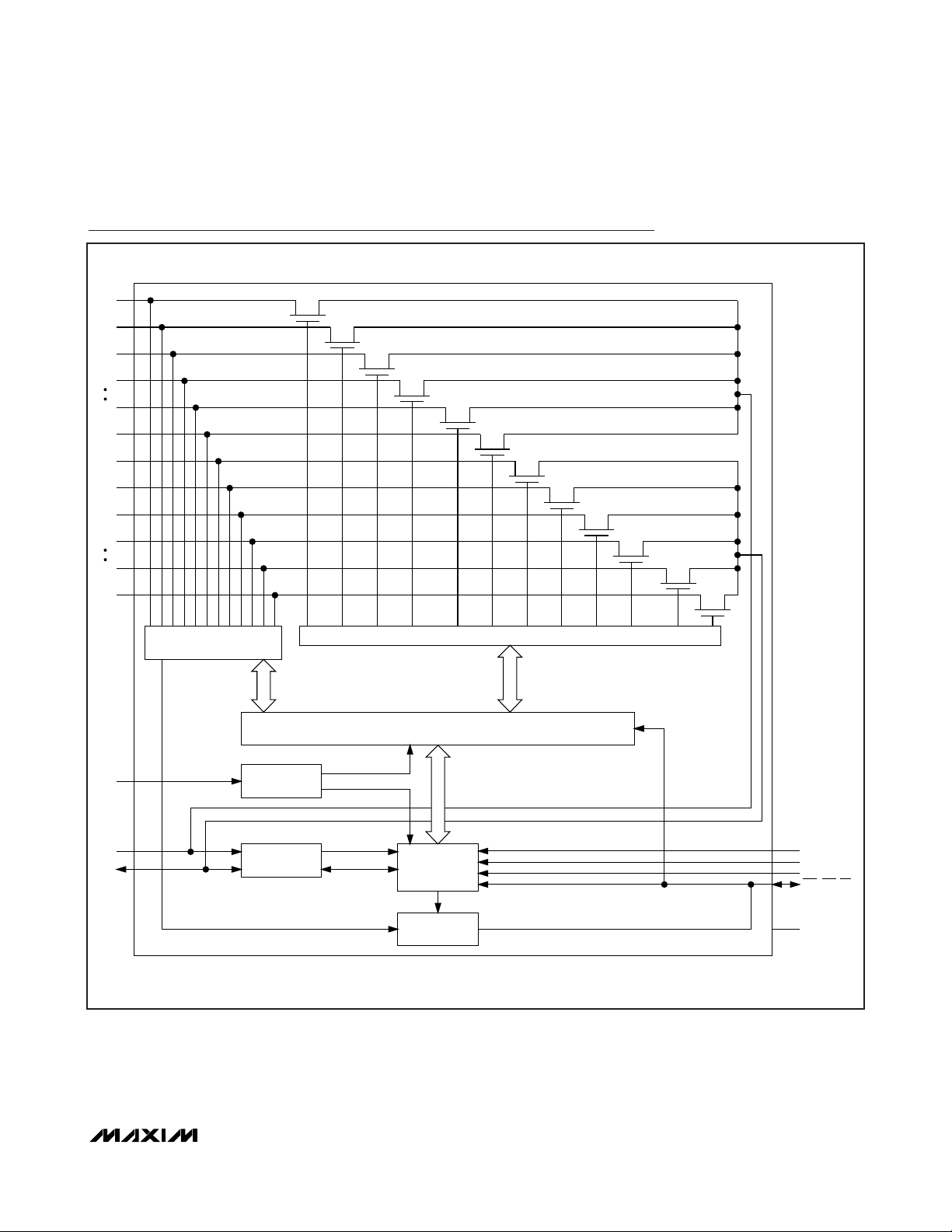
Functional Diagram
SC0
SC1
SC2
SC3
SC6
SC7
SD0
SD1
SD2
SD3
SD6
SD7
LOCK-UP DETECTION
AND WIGGLE TEST
SWITCH ENABLE/DISABLE
V
DD
SCL
SDA
( ) ONLY FOR THE MAX7357 AND MAX7358
POWER-ON
RESET
GLITCH FILTER
REGISTER BANK WITH SWITCH CONTROL LOGIC
I2C BUS
CONTROL
INT LOGIC
A0
A1
A2
RST (RST/INT)
GND
Page 10

MAX7356/MAX7357/MAX7358
1-to-8 I2C Bus Switches/Multiplexers with Bus
Lock-Up Detection, Isolation, and Notification
10 ______________________________________________________________________________________
Detailed Description
The MAX7356/MAX7357/MAX7358 devices are 1-to-8
I
2
C multiplexers/switches for connecting a large num-
ber of I
2
C components to a single master. The circuits
connect a main I
2
C bus to any combination of 8 extended I2C buses. They enable a master on the main bus to
isolate and communicate with devices or groups of
devices that may otherwise have slave address conflicts. Any extended bus can be connected or disconnected by control packets from the main I2C bus writing
to the main control register of these I2C switches.
The MAX7357/MAX7358 feature a built-in timer used to
monitor all extended buses, for lock-up conditions. If the
data line of any of these buses is low for more than
25ms, a lock condition is detected. An optional interrupt
can be generated through the bidirectional RST/INT pin.
The master can read the bus lock-up register to find out
which extended bus is locked up. The master can also
optionally enable the MAX7357 or MAX7358 to send a
flush-out sequence on the faulty channel. There is an
optional preconnection check that can be enabled,
which toggles the extended bus clock and data line low
then high to ensure that the downstream bus is not
locked high prior to connecting it to the host bus.
The bus lock-up detection and isolation features are
enabled by writing a unique series of I2C commands to
the MAX7357/MAX7358.
Power-On Reset
When power is applied to VDD, an internal power-on
reset (POR) holds the MAX7356/MAX7357/MAX7358 in
a reset state until VDDhas reached V
POR
. At this point,
the reset condition is released and the MAX7356/
MAX7357/MAX7358 registers and I2C state machine
are initialized to their default states.
Basic Mode of Operation
The MAX7356/MAX7357/MAX7358 feature a basic
mode of operation. In basic mode, the device operates
solely as a collection of analog switches that enable
any combination of the extended buses (SC_, SD_)
to be connected to the host-side bus (SCL, SDA). Only
the switch control register is accessible in basic mode
of operation.
Enhanced Mode of Operation
(MAX7357/MAX7358)
The MAX7357 and MAX7358 feature an enhanced
mode of operation that enable features and registers
that are unavailable in the basic mode of operation.
When operating in enhanced mode, there are 7 registers available to the host. Features such as bus lock-up
detection, preconnection fault tests, and diagnostic
information are made available to the user. A special
sequence of commands can switch the MAX7357 or
MAX7358 from basic mode to enhanced mode, and a
simple write to the configuration register can switch the
devices from enhanced mode back to basic mode.
Entering Basic Mode from
Enhanced Mode
(MAX7357/MAX7358)
When the 7 registers of Table 2 are enabled, the
MAX7357 and MAX7358 can be put into basic mode by
setting bit B6 of the configuration register. When basic
mode is entered, the value of all registers return to their
POR value. B6 of the configuration register is also maintained to allow operation in basic mode. When in basic
mode, the MAX7357 and MAX7358 can be returned to
full feature mode by receiving a special sequence of
commands from the host as described below.
The sequence of I2C commands for enabling the
MAX7357 or MAX7358 enhanced features (bus lock-up
detection, isolation, and notification) as well as access
to the additional 6 registers consists of a write byte, a
read byte, another write byte, and another read byte
with no data bytes following any of these write or read
bytes, as shown in Figure 5. A write byte consists of
the 7-bit MAX7357 or MAX7358 device address followed by a 0. A read byte consists of the 7-bit
MAX7357 or MAX7358 device address followed by a 1.
The special sequence begins with a START condition
and ends with a STOP condition. Repeated START
conditions are used to interconnect these write and
read bytes.
The complete special sequence of I2C commands
needs to be received by the MAX7357 or MAX7358 to
activate the enhanced mode.
Figure 5. The Special Sequence of I2C Commands for Turning on the Full Feature
ACKNOWLEDGE FROM THE
MAX7357 OR MAX7358
ADDRESS OF MUX/SWT PARTS
START
0 A Sr ADDRESS OF MUX/SWT PART 0 A SrADDRESS OF MUX/SWT PART 1 A Sr ADDRESS OF MUX/SWT PART 1 A P
W
ACKNOWLEDGE FROM THE
MAX7357 OR MAX7358
R
ACKNOWLEDGE FROM THE
MAX7357 OR MAX7358
W
ACKNOWLEDGE FROM THE
MAX7357 OR MAX7358
R
STOP
Page 11

MAX7356/MAX7357/MAX7358
1-to-8 I2C Bus Switches/Multiplexers with Bus
Lock-Up Detection, Isolation, and Notification
______________________________________________________________________________________ 11
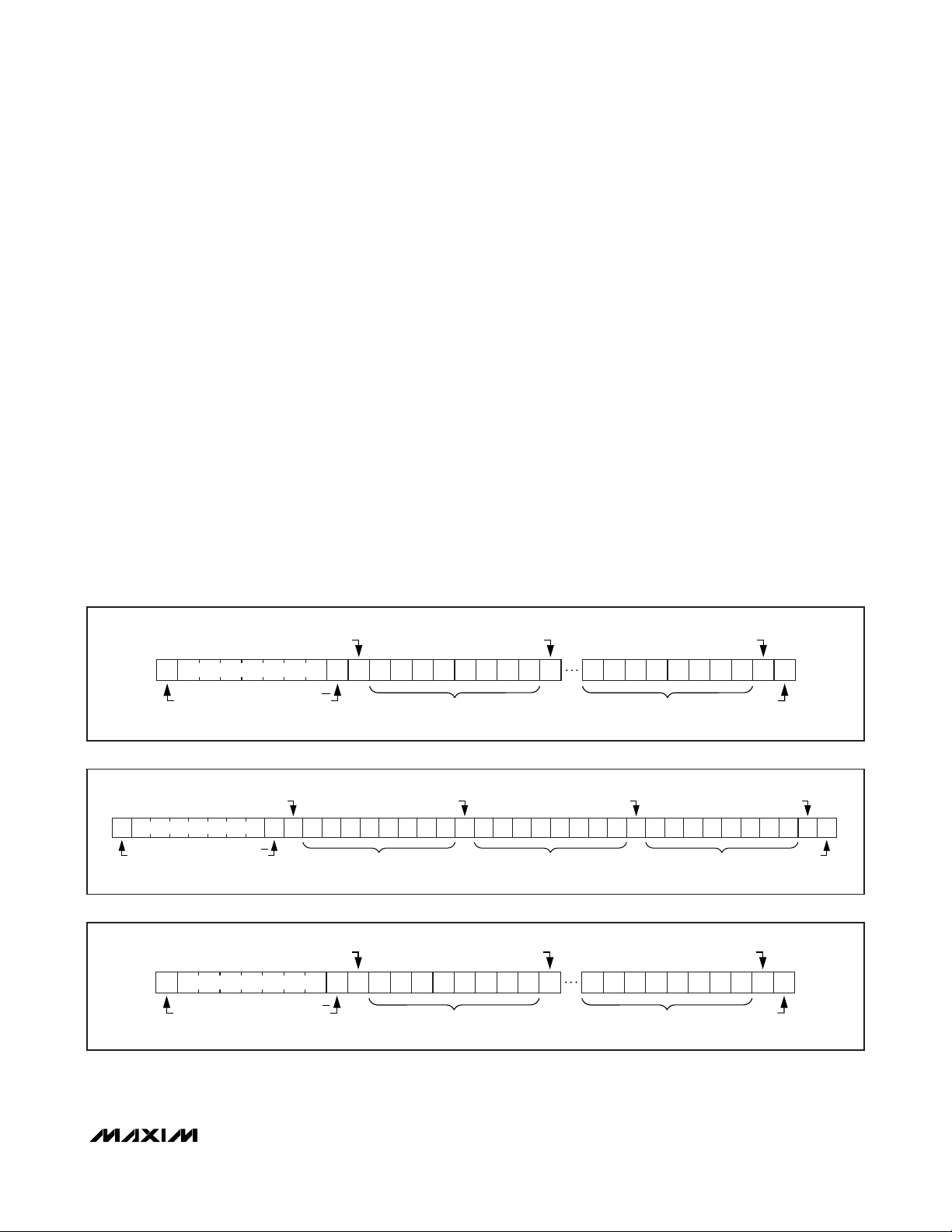
Bus Lock-Up Detection, Isolation,
and Notification Operation
(MAX7357/MAX7358)
SDA Stuck Low
If either line of any downstream bus is low for a period
exceeding 25ms between t1and t2in Figure 6, the
MAX7357/MAX7358 detect a lock-up fault on that bus
and takes the action configured by the user. If the lockup is not on the main bus, SDA and SCL return to the
high state at the same time. The MAX7357 or MAX7358
then identifies which SD_ or SC_ is still pulled low. If the
optional interrupt function is enabled (by setting B0 of
the configuration register), an active-low interrupt is
generated at RST/INT.
If B4 in the configuration register is set to 1, then only
faults on connected buses cause the MAX7357 or
MAX7358 to disconnect all buses from each other.
When this is the case, faults detected on disconnected
buses set the flag in the lock-up status register, and, if
enabled, notify the host of the fault, but do not disconnect the buses from one another.
B1 of the configuration register enables the flush-out
sequence. If this bit is set to 1, the MAX7357 or
MAX7358 attempts to send a flush-out sequence over
the locked SD_ and SC_ pair (the sequence begins at
t
5
in Figure 6). If the flush-out sequence is successful,
the locked bus (SD_ and SC_) is released at t
6
(Figure
6). The I2C master (at SDA and SCL) reads the
MAX7357 or MAX7358 lock-up status register to identify the locked-up bus. If RST/INT is enabled as an
interrupt, it is released once a read command to the
lock-up indication register is received by the MAX7357
or MAX7358 (shown at t7in Figure 6). The RST/INT
can also be automatically released after a 1.6s delay
by setting bit 2 of the configuration register.
Preconnection Wiggle Test
(Stuck High Fault)
(MAX7357/MAX7358)
By setting bit B7 in the configuration register to 1, a preconnection wiggle test is enabled for all downstream
buses. This test only runs on the downstream bus when
the bus is selected through the switch control register.
Enabling this test does not affect any bus that is already
connected to the host bus; however, deselecting and
subsequently reselecting the bus will cause the test to
occur. The test is performed when the switch control register bit (or bits if multiple buses are selected in the same
I2C transaction) toggles from 0 to 1 and a stop condition
is received. It consists of the MAX7357 or MAX7358
pulling the downstream clock line low, then the downstream data line low. Both lines are checked for a nominal low value, and then the clock line is released followed
by the data line (Note: This is an I
2
C stop condition and
is seen by any I2C devices connected to the extended
bus). If either the clock or data line (or both) fail to pull
low during the test, the MAX7357 or MAX7358 do not
allow that downstream bus to connect to the host. If the
optional interrupt notification bit is set (B0), the device
notifies the host that a fault has occurred. The I2C master
can then read the MAX7357 or MAX7358 registers to find
out which bus or buses caused the fault. Faults detected
by this test are stored in the preconnection fault register
(0x06). The stuck high Fault register is cleared once this
register is read, resetting the device, or disabling the
preconnection test.
Device Address
The MAX7356/MAX7357/MAX7358 family of devices
has selectable device addresses through three external
inputs. The slave address consists of 4 fixed bits
(A6–A3 set to 1110); followed by 3 pin-programmable
bits (A2, A1, A0), as shown in Figure 7. The addresses
A2, A1, and A0 can also be driven dynamically if
required, but the values must be stable when they are
expected in the address sequence.
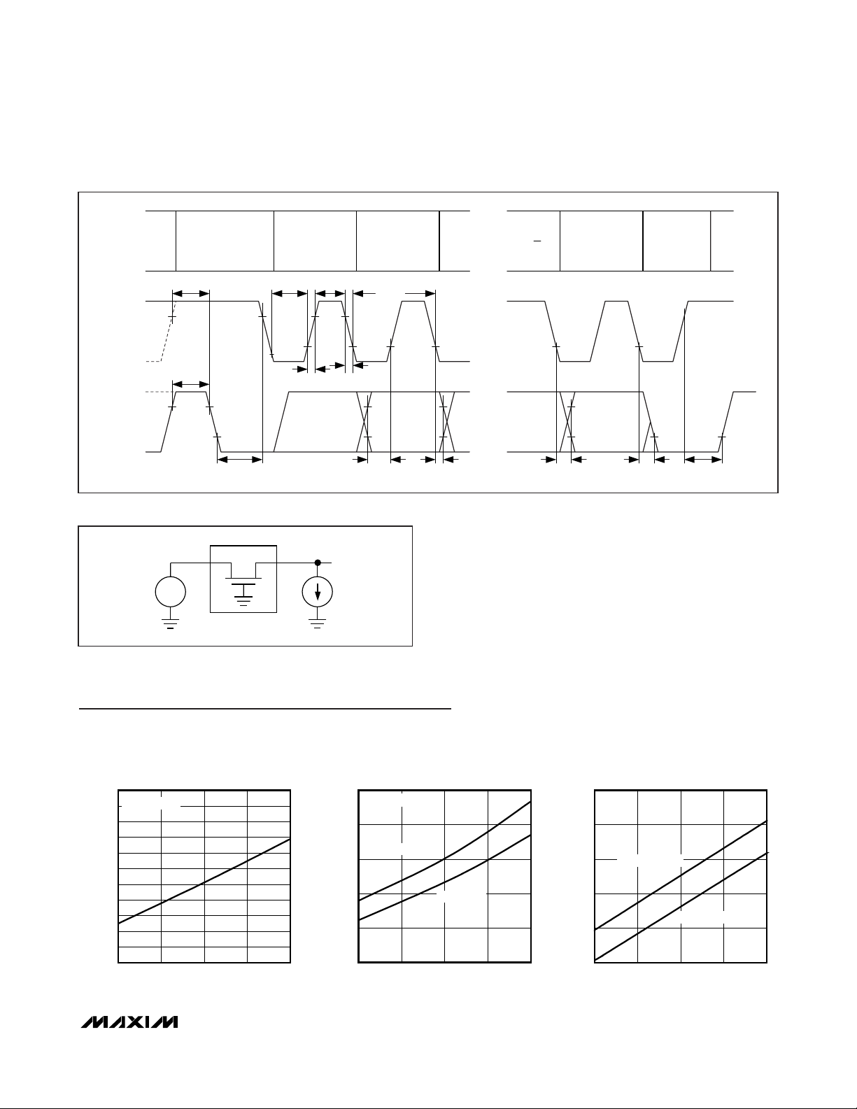
Figure 6. Bus Lock-Up Detection, Isolation, and Notification Timing Diagram
t
3
t
t
5
t
4
2
NOTE: THE FLUSH-OUT SEQUENCE RUNS AT AN SC_ FREQUENCY OF 40kHz.
THE HOST MAY COMMUNICATE AT UP TO 400kHz. THE TIMING SHOWN IS NOT TO SCALE.
t
SDA
SCL
SD_
SC_
RST/INT
t
1
6
BYTE1
FLUSH-OUT DATA
BYTE4
t
7
Page 12
MAX7356/MAX7357/MAX7358
1-to-8 I2C Bus Switches/Multiplexers with Bus
Lock-Up Detection, Isolation, and Notification
12 ______________________________________________________________________________________
Available addresses depend on the hardware connections of pins A2, A1, and A0 as shown in Table 1.
The last bit following the slave address bit A0 on an I
2
C
command defines the operation to be performed. When
the last bit sets to logic 1, a read is selected while logic
0 selects a write operation.
Register Map (MAX7357/MAX7358)
The MAX7357 and MAX7358 have 7 registers (shown in
Table 2) that can be accessed through the I2C bus. The
MAX7357 powers up with all of these registers accessible. The initial register address counter is at 0x00. The
MAX7358 powers up in basic mode with only the switch
control register available. Writing to a MAX7358
changes only the contents of the switch control register.
By sending a unique I2C sequence to the MAX7358, all
7 registers become available.
Register Access Protocol (MAX7356)
Only the MAX7356 device address is required to gain
access to its registers. A typical I2C command to communicate with the MAX7356 starts with its device
address followed directly by data bytes.
Figure 7. MAX7356/MAX7357/MAX7358 Slave Address
Table 1. MAX7356/MAX7357/MAX7358 Switch Multiplexer Device Address
Table 3. MAX7357 and MAX7358 BasicMode Register Map
Table 2. MAX7357/MAX7358 Enhanced-Mode Register Map
PIN-SELECTABLE BITS
A5 R/WA6 A4 A3 A2 A1 A0
FIXED
A2
CONNECTION
GND GND GND 1110000
GND GND V
GND V
GND V
V
DD
V
DD
V
DD
V
DD
A1
CONNECTION
DD
DD
GND GND 1110100
GND V
V
DD
V
DD
A0
CONNECTION
DD
GND 1110010
V
DD
DD
GND 1110110
V
DD
A6 A5 A4 A3 A2 A1 A0
1110001
1110011
1110101
1110111
REGISTER NAME
Switch Control 0x00 0 0 0 0 0 0 0 0 0x01 R/W
Configuration 0x01 0 0 0 0 0 0 0 1 0x02 R/W
Flush-Out Sequence 0x02 1 1 1 1 1 1 1 1
Lock-Up Indication 0x03 0 0 0 0 0 0 0 0 0x04 R
Traffic Prior to Lock-Up
Stuck High Fault 0x06 0 0 0 0 0 0 0 0 0x00 R
INTERNAL
ADDRESS
0x04 0 0 0 0 0 0 0 0 0x05 R
0x05 0 0 0 0 0 0 0 0 0x06 R
B7 B6 B5 B4 B3 B2 B1 B0
POR DEFAULT SETTING
NEXT
ADDRESS
0x00 (W)
0x03 (R)
REGISTER
NAME
Switch
Control
POR DEFAULT SETTING
B7 B6 B5 B4 B3 B2 B1 B0
00000000 R/W
ACCESS
ACCESS
R/W
Page 13
MAX7356/MAX7357/MAX7358
1-to-8 I2C Bus Switches/Multiplexers with Bus
Lock-Up Detection, Isolation, and Notification
______________________________________________________________________________________ 13
Only the switch control register can be accessed through
an I2C write or read command. All data bytes are for
the switch control register. The last data byte in an I2C
write command is retained by the switch control register.
Register Access Protocol
(MAX7357/MAX7358)
Only the MAX7357 or MAX7358 I2C device address is
required to gain access to its registers. A typical I2C
command to communicate with the MAX7357 or
MAX7358 starts with its device address and is followed
directly by data bytes. Internal register addresses are
not used in an I2C write or read command.
For enhanced mode, all registers are accessed in
sequence starting with the switch control register and
follows the order defined by internal register addresses
as shown in Table 2. Internal register addresses are
0x00, 0x01, 0x02, 0x03, 0x04, 0x05, and 0x06 for
switch control, configuration, flush-out sequence, lockup indication, first and second bytes of the traffic prior
to lock-up, and preconnection fault registers, respectively. When writing data to the register(s), addressing
starts with address 0x00 and goes one higher in each
subsequent byte and comes back to 0x00 again after
0x02 since the next four higher addressed registers are
read only. Read access also starts with the internal register address 0x00 and goes one higher in each subsequent byte and comes back to 0x00 again after 0x06.
For basic mode, only the switch control register can be
accessed through an I2C write or read command. All
data bytes are for the switch control register. The last
data byte in an I2C write command is retained by the
switch control register. Incomplete bytes are ignored.
Switch Control Register
The switch control register (Figure 8) selects which
channels will be connected to the main I2C bus. This
register can be written and read through the main I2C
bus. The POR value for the switch control register is
0x00—all switches disconnected.
A SC_/SD_ downstream pair, or channel, is selected by
the contents of the switch control register. All bits of the
control byte are used to determine which channel is to
Figure 8. Switch Control Register
Table 4. Switch Control Register Channel Selection
X = Don’t care.
B7 B6 B5 B4 B3 B2 B1 B0 COMMAND
XXXXXXX 0Channel 0 disabled
XXXXXXX 1Channel 0 enabled
X X X X X X 0 X Channel 1 disabled
X X X X X X 1 X Channel 1 enabled
X X X X X 0 X X Channel 2 disabled
X X X X X 1 X X Channel 2 enabled
X X X X 0 X X X Channel 3 disabled
X X X X 1 X X X Channel 3 enabled
X X X 0 X X X X Channel 4 disabled
X X X 1 X X X X Channel 4 enabled
XX0XXXX XChannel 5 disabled
XX1XXXX XChannel 5 enabled
X0XXXXX XChannel 6 disabled
X1XXXXX XChannel 6 enabled
0XXXXXXXChannel 7 disabled
1XXXXXXXChannel 7 enabled
CHANNEL SELECTION BITS (READ/WRITE)
B6 B0B7 B5 B4 B3 B2 B1
CHANNEL 0
CHANNEL 1
CHANNEL 2
CHANNEL 3
CHANNEL 4
CHANNEL 5
CHANNEL 6
CHANNEL 7
Page 14

MAX7356/MAX7357/MAX7358
1-to-8 I2C Bus Switches/Multiplexers with Bus
Lock-Up Detection, Isolation, and Notification
14 ______________________________________________________________________________________
Table 5. Configuration Register Definition
X = Don’t care.
be selected. More than one channel can be selected
simultaneously. When a channel is selected, the channel
becomes active immediately after a stop condition has
been placed on the I2C bus. This ensures that all
SC_/SD_ lines are in a HIGH state when the channel is
made active, so that no false conditions are generated at
the time of connection.
Configuration Register
(MAX7357/MAX7358)
B0 = RST/INT serves as an interrupt when a bus lockup condition is detected.
B1 = Flush-out sequence is sent automatically on lockedup channels when a lock-up condition is detected.
B2 = When B0 = 1, release the RST/INT output after
asserting for 1.6 seconds.
B3 = Data in the lock-up indication register cleared only
after reading the register.
B4 = Connected channels remain connected on detection of lock-up if the lock-up condition is present only on
a channel that is not connected.
B5 = Disable bus lock-up detection.
B6 = Basic mode.
B7 = Enables the preconnection wiggle test for SC_
and SD_.
Flush-Out Sequence Register
(MAX7357/MAX7358)
A flush-out sequence can be sent to a particular auxiliary bus automatically after the identification of the lockup condition. The flush-out sequence consists of 18
SC_ clock cycles. An 8-bit sequence for the SD_ to follow during the flush-out cycle can also be defined by
writing to the flush-out sequence register. By default,
the flush-out sequence register is all ones. The
MAX7357 or MAX7358 attempt to send the one-byte
sequence followed by an additional clock cycle (NACK)
two times sequentially, followed by a stop condition.
The effectiveness of sending the flush-out sequence
depends on the behavior of the locked-up device. For
an auxiliary bus with only slave devices, it is more likely
that the SCL line can still be driven by the MAX7357 or
MAX7358. In this case, a slave device may respond to
a particular flush-out sequence. After the release of the
SD_ line by a “stuck” device, the remaining sequence
on the SD_ line can be used to reset itself.
Bus Lock-Up Indication Register
(MAX7357/MAX7358)
The bus master can read the lock-up indication byte to
identify the stuck channels. A bit set to ”1” indicates
that the associated channel is stuck. The indication for
a given channel remains as long as the lock-up condi-
B7 B6 B5 B4 B3 B2 B1 B0 COMMAND
XXXXXXX0Interrupt with RST/INT disabled
XXXXXXX1Interrupt with RST/INT enabled
XXXXXX0XFlush-out disabled
XXXXXX1XFlush-out enabled
XXXXX0XXRST/INT released after a register read
XXXXX1XXRST/INT released after 1.6 seconds
XXXX0XXX
XXXX1XXX
X X X 0 X X X X Disconnect all channels on bus lock-up
X X X 1 X X X X Disconnect only the locked up bus
X X 0 X X X X X Bus lock-up detection enabled
X X 1 X X X X X Bus lock-up detection disabled
X0XXXXXXEnhanced mode
X1XXXXXXBasic mode enabled
0XXXXXXXPreconnect test is disabled
1XXXXXXXPreconnect test is enabled
The lock-up register shows the current
condition
The lock-up register data is not cleared
until a read
Page 15

MAX7356/MAX7357/MAX7358
1-to-8 I2C Bus Switches/Multiplexers with Bus
Lock-Up Detection, Isolation, and Notification
______________________________________________________________________________________ 15
tion exists on that channel. If the interrupt feature is
selected (B0 of the configuration register is 1), however, the interrupt signal, RST/INT, deasserts (goes to
high) once this bus lock-up indication register is read.
If desired, setting bit B3 of the configuration register to
1 can latch the lock-up data. When B3 is set, the lockup bits remain set (even if a channel becomes
“unstuck”) until the lock-up indication register is read
by the master. Lock-up conditions on unconnected auxiliary buses are also detected. When this happens, operation is the same as when lock-ups are detected on
connected buses, except that, if desired, bus connections may be maintained as long as any detected lockups are present only on unconnected channels. This
option is selected using bit B4 of the configuration register. (Figure 9)
Traffic Prior to Lock-Up Register
(MAX7357/MAX7358)
The I2C bus traffic information per SCL clock is monitored and stored into the two-byte traffic prior to lock-up
register. The first two bytes of information after a START
are stored in this register. This I
2
C bus traffic information is frozen upon a bus lock-up detection. A host can
read these two bytes of traffic information upon the
reception of an interrupt signal. The contents of the traffic prior to lock-up register is released and refreshed
once it is read.
The traffic prior to lock-up register can be used to identify the device address as well as the following byte
involved in a bus lock-up.
When troubleshooting an I2C bus, a scope is usually
used to capture traffic leading to the problem. The contents of the traffic prior to the bus fault can usually be
determined by identifying a device address, a register
address, or a part of this data.
Table 7 shows contents of the traffic prior to the lock-up
register corresponding to a lock-up situation as demonstrated by Figure 10.
Figure 9. Lock-Up Indication Bits
Table 6. Lock-Up Register Channel Indication
X = Don’t care.
B7 B6 B5 B4 B3 B2 B1 B0 COMMAND
XXXXXXX0Channel 0 no lock-up
XXXXXXX1Channel 0 lock-up
XXXXXX0XChannel 1 no lock-up
XXXXXX1XChannel 1 lock-up
X X X X X 0 X X Channel 2 no lock-up
X X X X X 1 X X Channel 2 lock-up
X X X X 0 X X X Channel 3 no lock-up
X X X X 1 X X X Channel 3 lock-up
X X X 0 X X X X Channel 4 no lock-up
X X X 1 X X X X Channel 4 lock-up
X X 0 X X X X X Channel 5 no lock-up
X X 1 X X X X X Channel 5 lock-up
X0XXXXXXChannel 6 no lock-up
X1XXXXXXChannel 6 lock-up
0XXXXXXXChannel 7 no lock-up
1XXXXXXXChannel 7 lock-up
CHANNEL LOCK-UP INDICATION BITS (READ)
B6 B0B7 B5 B4 B3 B2 B1
CHANNEL 0
CHANNEL 1
CHANNEL 2
CHANNEL 3
CHANNEL 4
CHANNEL 5
CHANNEL 6
CHANNEL 7
Page 16

MAX7356/MAX7357/MAX7358
1-to-8 I2C Bus Switches/Multiplexers with Bus
Lock-Up Detection, Isolation, and Notification
16 ______________________________________________________________________________________
Table 8. Stuck HIGH Fault Register Channel Indication
X = Don’t care.
Table 7. A Traffic Prior to Lock-Up Register Contents Example
Stuck HIGH Fault Register
(MAX7357/MAX7358)
Following an interrupt when bit B0 and B7 are enabled,
the bus master can read the stuck high fault byte to
identify stuck channels. A bit set to ”1” indicates that
the associated channel is stuck, and will not be allowed
to be connected to the host bus. The stuck high fault
register is cleared, and, if the interrupt feature is
enabled, RST/INT deasserts (goes to high) once this
register is read. However, while B7 is set to one, any
time a disconnected bus is selected for connection, the
preconnect test runs. If the fault still exists, the fault
handling sequence repeats and the faulty bus will not
be allowed to connect to the host bus.
RST
(MAX7356)
The RST on the MAX7356 can be used to reset the
MAX7356 by a host. The RST input is an active-low signal. By asserting this signal low for a minimum of t
WL(rst)
externally, the MAX7356 resets its I2C state machine
and deselects all channels. RST is overvoltage-tolerant
to +6V. The RST input must be connected to V
DD
through a pullup resistor.
RST/INT
(MAX7357/MAX7358)
The RST/INT on the MAX7357 or MAX7358 is bidirectional. It can be used to reset the device by a host or by
the device to send an interrupt signal to the host. The
RST/INT input is an active-low signal. By asserting
RST/INT low for a minimum of t
WL(rst)
externally, the
device resets its registers and I2C state machine and
deselects all channels. When RST/INT is configured to
notify the host of fault conditions, and while RST/INT
is being used as an output by the MAX7357 or
MAX7358 (sending an interrupt to the host), it does not
function as a reset input. RST/INT is overvoltage-tolerant
to +6V. RST/INT must be connected to VDDthrough a
pullup resistor.
Interrupt Signal (MAX7357/MAX7358)
A bus lock-up-caused interrupt signal can be sent to a
host through the bidirectional RST/INT pin depending
on whether or not bit B0 of the configuration register is
set. Configuration register bit B2 controls how the interrupt signal is reset. When B2 = 0, the interrupt signal
asserts (stays low) until the lock-up indication register is
read. When B2 = 1, the interrupt signal deasserts after
ADDRESS B7 B6 B5 B4 B3 B2 B1 B0 NOTE
0x04 0 1 1 01000Write to the troubled device address
0x05 0 1 1 00000The first data byte with trailing 0’s due to lock-up
B7 B6 B5 B4 B3 B2 B1 B0 COMMAND
XXXXXXX0Channel 0 not stuck high
XXXXXXX1Channel 0 stuck high
XXXXXX0XChannel 1 not stuck high
XXXXXX1XChannel 1 stuck high
X X X X X 0 X X Channel 2 not stuck high
X X X X X 1 X X Channel 2 stuck high
X X X X 0 X X X Channel 3 not stuck high
X X X X 1 X X X Channel 3 stuck high
X X X 0 X X X X Channel 4 not stuck high
X X X 1 X X X X Channel 4 stuck high
X X 0 X X X X X Channel 5 not stuck high
X X 1 X X X X X Channel 5 stuck high
X0XXXXXXChannel 6 not stuck high
X1XXXXXXChannel 6 stuck high
0XXXXXXXChannel 7 not stuck high
1XXXXXXXChannel 7 stuck high
Page 17

MAX7356/MAX7357/MAX7358
1-to-8 I2C Bus Switches/Multiplexers with Bus
Lock-Up Detection, Isolation, and Notification
______________________________________________________________________________________ 17
2 seconds. The interrupt signal asserts again once a
new lock-up is detected. The interrupt signal does not
activate the reset function.
Serial Interface
Serial Addressing
The MAX7356/MAX7357/MAX7358 operate as a slave
that sends and receives data through an I
2
C interface.
The interface uses a serial-data line (SDA) and a serialclock line (SCL) to achieve bidirectional communication
between master(s) and slave(s). The master initiates all
data transfers to and from the MAX7357 or MAX7358
and generates the SCL clock that synchronizes the
data transfer.
SDA operates as both an input and an open-drain output. A pullup resistor (4.7kΩ, typ) is required on SDA.
SCL operates only as an input. A pullup resistor (4.7kΩ,
typ) is required on SCL if there are multiple masters on
the 2-wire interface, or if the master in a single-master
system has an open-drain SCL output.
Each transmission consists of a START condition sent
by a master, followed by the MAX7356/MAX7357/
MAX7358’s 7-bit slave address plus R/W bit, and then
optionally 1 or more data bytes, and finally a STOP condition (Figure 10).
START and STOP Conditions
Both SCL and SDA remain high when the interface is
not busy. The master signals the beginning of a transmission with a START (S) condition by transitioning SDA
from high to low while SCL is high. When the master
has finished communicating with the slave, the master
issues a STOP (P) condition by transitioning SDA from
low to high while SCL is high. The bus is then free for
another transmission (Figure 11).
Bit Transfer
One data bit is transferred during each clock pulse.
The data on SDA must remain stable while SCL is high
(Figure 12).
Acknowledge
The acknowledge bit is a clocked 9th bit the recipient
uses to handshake receipt of each byte of data (Figure
13). Each byte transferred effectively requires 9 bits.
The master generates the 9th clock pulse, and the
recipient pulls down SDA during the acknowledge
clock pulse, so the SDA line is stable low during the
high period of the clock pulse. When the master is
transmitting to the MAX7356/MAX7357/MAX7358, the
MAX7356/MAX7357/MAX7358 generate the acknowl-
Figure 10. Bus Lock-Up During a 3-Byte Write Command
Figure 11. Start and Stop Conditions
Figure 12. Bit Transfer
Figure 13. Acknowledge
ACKNOWLEDGE FROM
THE TROUBLED DEVICE
0 A 01 0 01 1 0S 0 0 L L L L L L L L L L L L L L L1 1
LOCK-UP
OCCURS
START
SDA
SCL
S
START
CONDITION
SDA
SCL
DATA STABLE
DATA VALID
START
CONDITION
SCL
SDA
12 8 9
CHANGE OF
DATA ALLOWED
W
CONDITION
CLOCK PULSE FOR
ACKNOWLEDGMENT
NOT ACKNOWLEDGE
ACKNOWLEDGE
FIRST DATA BYTE SECOND DATA BYTE
P
STOP
Page 18

MAX7356/MAX7357/MAX7358
1-to-8 I2C Bus Switches/Multiplexers with Bus
Lock-Up Detection, Isolation, and Notification
18 ______________________________________________________________________________________
edge bit because the device is the recipient. When the
MAX7356/MAX7357/MAX7358 are transmitting to the
master, the master generates the acknowledge bit
because the master is the recipient.
Slave Address
The MAX7356/MAX7357/MAX7358 have 7-bit-long
slave addresses (Figure 6). The eighth bit following the
7-bit slave address is the R/W bit. It is low for a write
command, and high for a read command.
Accessing the MAX7356
A single-byte write to the MAX7356 sets the switch
control register.
A multibyte write to the MAX7356 writes repeatedly to
the switch control register. The last byte written determines the contents of the register.
A single-byte read from the MAX7356 returns the con-
tents of the switch control register.
A multibyte read (2 or more bytes before the I2C STOP
bit) from the MAX7356 returns the contents of the
switch control register repeatedly.
Accessing the MAX7357/MAX7358 in
Enhanced Mode
In enhanced mode, all 7 registers are enabled. These
registers are autoincremented starting with the switch
control register during each I2C transaction. When a
new transaction begins, the switch control register is
the first register accessed.
A single-byte write to the MAX7357 or MAX7358 sets
the switch control register.
A 2-byte write to the MAX7357 or MAX7358 sets the
switch control and configuration registers.
A 3-byte write to the MAX7357 or MAX7358 sets the
switch control, configuration, and flush-out sequence
registers.
A multibyte write to the MAX7357 or MAX7358 with
more than three bytes sets the first three registers, then
resets the pointer back to the switch control register
(0x00) since the remaining registers are read only.
Subsequent bytes of data, after 3 bytes, begin overwriting the first set of data starting with 0x00, 0x01, 0x02,
then looping back to 0x00 again, and continuing until a
STOP condition is received.
A single-byte read from the MAX7357 or MAX7358
returns the contents of the switch control register.
A multibyte read from the MAX7357 or MAX7358 returns
contents of all 7 registers in sequence and repeats.
The internal register address count always begins with
the switch control register, 0x00.
Accessing the MAX7357/MAX7358
in Basic Mode
In basic mode, only the switch control register is
enabled.
A single-byte write to the MAX7357 or MAX7358 sets
the switch control register.
A multibyte write to the MAX7357 or MAX7358 in basic
mode writes repeatedly to the switch control register.
The last byte written determines the contents of the register.
A single-byte read from the MAX7357 or MAX7358
returns the contents of the switch control register.
A multibyte read (2 or more bytes before the I
2
C STOP
bit) from the MAX7357 or MAX7358 returns the contents
of the switch control register repeatedly.
Writing to the MAX7356
The MAX7356’s switch control register can be written by
an I2C write command starting with the device address
for the MAX7356 and followed by data bytes. The last
data byte is stored into the switch control register.
A write to the MAX7356 starts with the master transmitting
the slave address with the R/W bit set low. The MAX7356
acknowledges the slave address. The master can then
issue a STOP condition after the acknowledge (Figure 14),
but typically the master proceeds to transmit one or more
bytes of data. The MAX7356 acknowledges these subsequent bytes of data and updates the switch control register when the master issues a STOP condition (Figure 14).
Writing to the MAX7357/MAX7358 in
Enhanced Mode
The MAX7357 and MAX7358 registers can be written
by an I2C write command starting with the device
address for the MAX7357 or MAX7358 and followed by
data bytes. The first data byte is stored into the switch
control register and subsequent data bytes are stored
into the subsequent registers.
A write to the MAX7357 or MAX7358 starts with the
master transmitting the slave address with the R/W bit
set low. The MAX7357 or MAX7358 acknowledge the
slave address. The master can then issue a STOP condition after the acknowledge (Figure 15), but typically
Page 19
MAX7356/MAX7357/MAX7358
1-to-8 I2C Bus Switches/Multiplexers with Bus
Lock-Up Detection, Isolation, and Notification
______________________________________________________________________________________ 19
the master proceeds to transmit one or more bytes of
data. The MAX7357 or MAX7358 acknowledge these
subsequent bytes of data and update corresponding
registers with each new byte until the master issues a
STOP condition (Figure 15).
Writing to the MAX7357/MAX7358
in Basic Mode
The MAX7357 and MAX7358 switch control register can
be written by an I2C write command starting with the
device address for the MAX7357 or MAX7358 and followed by data bytes. The last data byte is stored in the
switch control register.
A write to the MAX7357 or MAX7358 starts with the
master transmitting the slave address with the R/W bit
set low. The device acknowledges the slave address.
The master can then issue a STOP condition after the
acknowledge (Figure 16), but typically the master proceeds to transmit one or more bytes of data. The
MAX7357 or MAX7358 acknowledge these subsequent
bytes of data and update the switch control register
when the master issues a STOP condition (Figure 16).
Reading from the MAX7356
A read from the MAX7356 starts with the master transmitting the slave address with the R/W bit set high. The
MAX7356 acknowledges the slave address. The master
can read 1 byte from the switch control register and
then issue a STOP condition (Figure 17). If the master
reads more than one byte, the master upon reception
acknowledges each byte. All bytes return the contents
of the switch control register.
Reading from the MAX7357/MAX7358
in Enhanced Mode
A read from the MAX7357 or MAX7358 starts with the
master transmitting the slave address with the R/W bit
set high. The device acknowledges the slave address.
The master can read 1 byte from the device and then
issue a STOP condition (Figure 18). In this case, the
device transmits the data byte from the switch control
register. Typically, the master reads 1 or 2 bytes with
each byte being acknowledged by the master upon
reception. The first data byte comes from the switch
control register and subsequent data bytes come from
the subsequent registers in order.
Figure 14. Writing to the MAX7356
Figure 15. Writing to the MAX7357 or MAX7358 in Enhanced Mode
ADDRESS OF MUX/SWT PARTS
START
0 A D7 D6 D5 D4 D3 D2 D1 D0 A P
R/W
ACKNOWLEDGE FROM THE
MAX7357 OR MAX7358
ACKNOWLEDGE FROM THE
MAX7357 OR MAX7358
STOP
DATA BYTE TO THE SWITCH
CONTROL REGISTER
D7 D6 D5 D4 D3 D2 D1 D0 A
ACKNOWLEDGE FROM THE
MAX7357 OR MAX7358
DATA BYTE TO THE SWITCH
CONTROL REGISTER
Figure 16. Writing to the MAX7357 or MAX7358 in Basic Mode
ACKNOWLEDGE FROM THE
ADDRESS OF MUX/SWT PARTS
MAX7356
0 A D7 D6 D5 D4 D3 D2 D1 D0 A P
ACKNOWLEDGE FROM THE
MAX7356
D7 D6 D5 D4 D3 D2 D1 D0 A
ACKNOWLEDGE FROM THE
MAX7356
START
R/W
DATA BYTE TO THE SWITCH
CONTROL REGISTER
START
ACKNOWLEDGE FROM THE
ADDRESS OF MUX/SWT PARTS
MAX7357 OR MAX7358
0 A D7 D6 D5 D4 D3 D2 D1 D0 A
R/W
ACKNOWLEDGE FROM THE
MAX7357 OR MAX7358
DATA BYTE TO THE SWITCH
CONTROL REGISTER
DATA BYTE TO THE SWITCH
ACKNOWLEDGE FROM THE
D7 D6 D5 D4 D3 D2 D1 D0 A
DATA BYTE TO THE CONFIGURATION
REGISTERS
MAX7358
CONTROL REGISTER
ACKNOWLEDGE FROM THE
D7 D6 D5 D4 D3 D2 D1 D0 A
DATA BYTE TO THE FLUSH-OUT
SEQUENCE
STOP
MAX7358
P
STOP
Page 20

MAX7356/MAX7357/MAX7358
1-to-8 I2C Bus Switches/Multiplexers with Bus
Lock-Up Detection, Isolation, and Notification
20 ______________________________________________________________________________________
Figure 17. Reading the MAX7356
ADDRESS OF MUX/SWT PARTS
START
1 A D7 D6 D1 D0 A P
R/W
ACKNOWLEDGE FROM THE
MAX7357 OR MAX7358
ACKNOWLEDGE
FROM A HOST
STOP
DATA BYTE FROM THE SWITCH
CONTROL REGISTER
DATA BYTE FROM
REGISTERS
0X01 TO 0X06
D7 D6 D5 D4 D3 D2 D1 D0 A
ACKNOWLEDGE FROM A
HOST
DATA BYTE FROM THE
STUCK HIGH FAULT REGISTER
Figure 18. Reading the MAX7357 or MAX7358 in Enhanced Mode
ADDRESS OF MUX/SWT PARTS
START
1 A D7 D6 D5 D4 D3 D2 D1 D0 A P
R/W
ACKNOWLEDGE FROM THE
MAX7357 OR MAX7358
ACKNOWLEDGE FROM A
HOST
STOP
DATA BYTE FROM THE SWITCH
CONTROL REGISTER
D7 D6 D5 D4 D3 D2 D1 D0 A
ACKNOWLEDGE FROM A
HOST
DATA BYTE FROM THE SWITCH
CONTROL REGISTER
Figure 19. Reading the MAX7357 or MAX7358 in Basic Mode
Reading from the MAX7357/MAX7358
in Basic Mode
A read from the MAX7357 or MAX7358 in basic mode
starts with the master transmitting the slave address
with the R/W bit set high. The device acknowledges the
slave address. The master can read 1 byte from the
switch control register and then issue a STOP condition
(Figure 19). If the master reads more than one byte, the
master upon reception acknowledges each byte. All
bytes return the contents of the switch control register.
Applications Information
Voltage Level Translation
The pass gates of the MAX7356/MAX7357/MAX7358
are designed so VDDcan be used to limit the voltage
levels transferred from one bus to another. The powersupply voltage of the part should be selected to be no
larger than one VGSON(0.7V, typ) above the lowest
bus voltage in the system. This ensures that the analog
switches do not allow current to flow from higher voltage buses to lower voltage buses.
Chip Information
PROCESS: CMOS
START
ACKNOWLEDGE FROM THE
MAX7357 OR MAX7358
ADDRESS OF MUX/SWT PARTS
0 A D7 D6 D5 D4 D3 D2 D1 D0 A P
R/W
ACKNOWLEDGE FROM THE
MAX7357 OR MAX7358
DATA BYTE TO THE SWITCH
CONTROL REGISTER
ACKNOWLEDGE FROM THE
MAX7357 OR MAX7358
D7 D6 D5 D4 D3 D2 D1 D0 A
DATA BYTE TO THE SWITCH
CONTROL REGISTER
STOP
Page 21

MAX7356/MAX7357/MAX7358
1-to-8 I2C Bus Switches/Multiplexers with Bus
Lock-Up Detection, Isolation, and Notification
______________________________________________________________________________________ 21
Typical Operating Circuit
Pin Configurations
V
CC
MASTER
SDA
SCL
RST
INT
SDA
SCL
RST(RST/INT)
GND
V
DD
V
DD
MAX7356
MAX7357
MAX7358
A0
A1
A2
SD0
SC0
SD1
SC1
SD7
SC7
V
DD
V
DD
V
DD
( ) ONLY FOR THE MAX7357 AND MAX7358
+
A0
MAX7356
MAX7357
MAX7358
TSSOP
( ) ONLY FOR THE MAX7357 AND MAX7358
241 V
232 SDAA1
223 SCLRST (RST/INT)
214A2SD0
205 SC7SC0
196 SD7SD1
187 SC6SC1
178 SD6SD2
169 SC5SC2
1510 SD5SD3
1411 SC4SC3
1312 SD4GND
DD
TOP VIEW
SD0
SC0
SD1
SC1
SD2
SC2
*CONNECT EXPOSED PAD TO GND.
( ) ONLY FOR THE MAX7357 AND MAX7358
RST
(RST/INT)
A1
2324 22 21
+
1
2
3
4
5
6
879
SC3
SD3
A0
MAX7356
MAX7357
MAX7358
10
GND
TQFN-EP
DD
V
SD4
SDA
SCL
19
20
18
A2
SC7
17
SD7
16
15
SC6
SD6
14
*EP
12
11
SC4
SD5
SC5
13
Page 22
MAX7356/MAX7357/MAX7358
1-to-8 I2C Bus Switches/Multiplexers with Bus
Lock-Up Detection, Isolation, and Notification
Maxim cannot assume responsibility for use of any circuitry other than circuitry entirely embodied in a Maxim product. No circuit patent licenses are
implied. Maxim reserves the right to change the circuitry and specifications without notice at any time.
22
____________________Maxim Integrated Products, 120 San Gabriel Drive, Sunnyvale, CA 94086 408-737-7600
© 2008 Maxim Integrated Products is a registered trademark of Maxim Integrated Products, Inc.
Package Information
For the latest package outline information and land patterns, go to www.maxim-ic.com/packages.
PACKAGE TYPE PACKAGE CODE DOCUMENT NO.
24 TSSOP U24+1
21-0066
24 TQFN-EP T2444+4
21-0139
 Loading...