

Page 1
General Description
The MAX7315 I2C™-/SMBus-compatible serial interfaced
peripheral provides microprocessors with 8 I/O ports.
Each I/O port can be individually configured as either an
open-drain current-sinking output rated at 50mA at 5.5V,
or a logic input with transition detection. A ninth port can
be used for transition detection interrupt or as a generalpurpose output. The outputs are capable of directly driving LEDs, or providing logic outputs with external
resistive pullup up to 5.5V.
PWM current drive is integrated with 8 bits of control.
Four bits are global control and apply to all LED outputs
to provide coarse adjustment of current from fully off to
fully on in 14 intensity steps. Each output then has individual 4-bit control, which further divides the globally
set current into 16 more steps. Alternatively, the current
control can be configured as a single 8-bit control that
sets all outputs at once.
The MAX7315 is pin and software compatible with the
PCA9534 and PCA9554(A).
Each output has independent blink timing with two blink
phases. All LEDs can be individually set to be on or off
during either blink phase, or to ignore the blink control.
The blink period is controlled by a register.
The MAX7315 is controlled through the 2-wire I2C/SMBus
serial interface, and can be configured to one of 64 I2C
addresses.
Applications
Features
♦ 400kbps, 2-Wire Serial Interface, 5.5V Tolerant
♦ 2V to 3.6V Operation
♦ Overall 8-Bit PWM LED Intensity Control
Global 16-Step Intensity Control
Plus Individual 16-Step Intensity Control
♦ Automatic Two-Phase LED Blinking
♦ 50mA Maximum Port Output Current
♦ Outputs Are 5.5V-Rated Open Drain
♦ Inputs Are Overvoltage Protected to 5.5V
♦ Transition Detection with Interrupt Output
♦ Low Standby Current (1.2µA typ; 3.3µA max)
♦ Tiny 3mm x 3mm, Thin QFN Package
♦ -40°C to +125°C Temperature Range
♦ All Ports Can Be Configured as Inputs or Outputs
MAX7315
8-Port I/O Expander with LED Intensity
Control and Interrupt
________________________________________________________________ Maxim Integrated Products 1
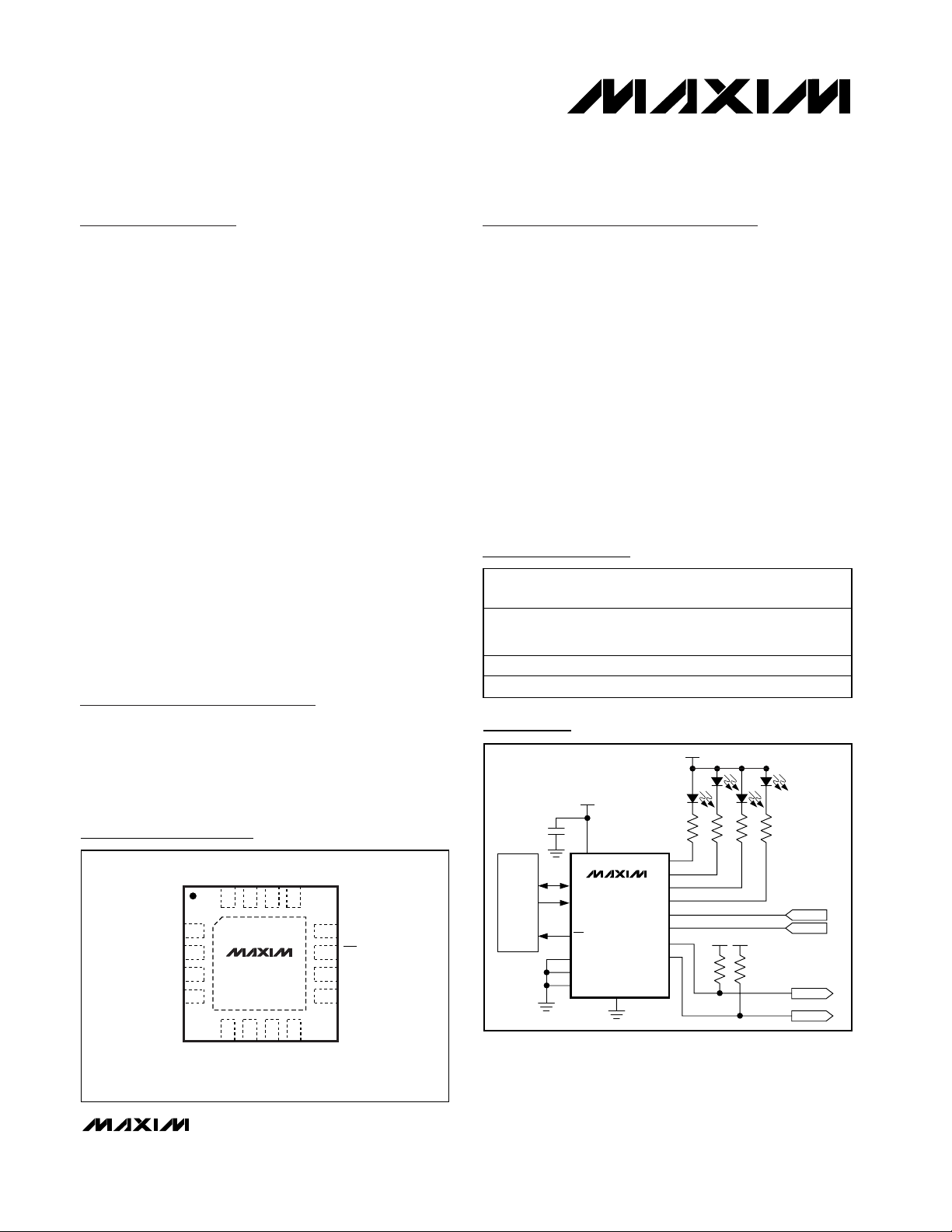
Pin Configurations
MAX7315
P5
P0
P1
P2
P3
V+
3.3V
µC
SDA
SCL
SDA
I/O
AD0
5V 3.3V
P6
P7
SCL
P4
OUTPUT2
OUTPUT1
GND
5V
INPUT 1
INPUT 2
AD2
AD1
0.047µF
INT/O8
Typical Application Circuit
19-3056; Rev 0; 10/03
For pricing, delivery, and ordering information, please contact Maxim/Dallas Direct! at
1-888-629-4642, or visit Maxim’s website at www.maxim-ic.com.
Ordering Information
Pin Configurations continued at end of data sheet.
LCD Backlights
LED Status Indication
Portable Equipment
Laptop Computers
Keypad Backlights
RGB LED Drivers
Cellular Phones
Purchase of I2C components of Maxim Integrated Products, Inc.,
or one of its sublicensed Associated Companies, conveys a
license under the Philips I
2
C Patent Rights to use these compo-
nents in an I
2
C system, provided that the system conforms to the
I
2
C Standard Specification as defined by Philips.
PART TEMP RANGE PIN-PACKAGE
MAX7315ATE -40°C to +125°C
MAX7315AEE -40°C to +125°C 16 QSOP —
MAX7315AUE -40°C to +125°C 16 TSSOP —
16 Thin QFN
3mm x 3mm x
0.8mm
TOP
MARK
AAU
TOP VIEW
AD2
1
2
P0
3
P1
4
P2
AD0
V+
GND
SDA
12
SCL
11
INT/O8
P7
10
P6
9
P4
P5
AD1
16 15 14 13
MAX7315ATE
5678
P3
QFN
Page 2
MAX7315
8-Port I/O Expander with LED Intensity
Control and Interrupt
2 _______________________________________________________________________________________
ABSOLUTE MAXIMUM RATINGS
Stresses beyond those listed under “Absolute Maximum Ratings” may cause permanent damage to the device. These are stress ratings only, and functional
operation of the device at these or any other conditions beyond those indicated in the operational sections of the specifications is not implied. Exposure to
absolute maximum rating conditions for extended periods may affect device reliability.
Voltage (with respect to GND)
V+ .............................................................................-0.3V to +4V
SCL, SDA, AD0, AD1, AD2, P0–P7 ..........................-0.3V to +6V
INT/O8 .....................................................................-0.3V to +8V
DC Current on P0–P7, INT/O8 ............................................55mA
DC Current on SDA.............................................................10mA
Maximum GND Current ....................................................190mA
Continuous Power Dissipation (T
A
= +70°C)
16-Pin TSSOP (derate 9.4mW/°C over +70°C) ............754mW
16-Pin QSOP (derate 8.3mW/°C over +70°C)..............666mW
16-Pin QFN (derate 14.7mW/°C over +70°C) ............1176mW
Operating Temperature Range (T
MIN
to T
MAX
)-40°C to +125°C
Junction Temperature......................................................+150°C
Storage Temperature Range .............................-65°C to +150°C
Lead Temperature (soldering, 10s) .................................+300°C
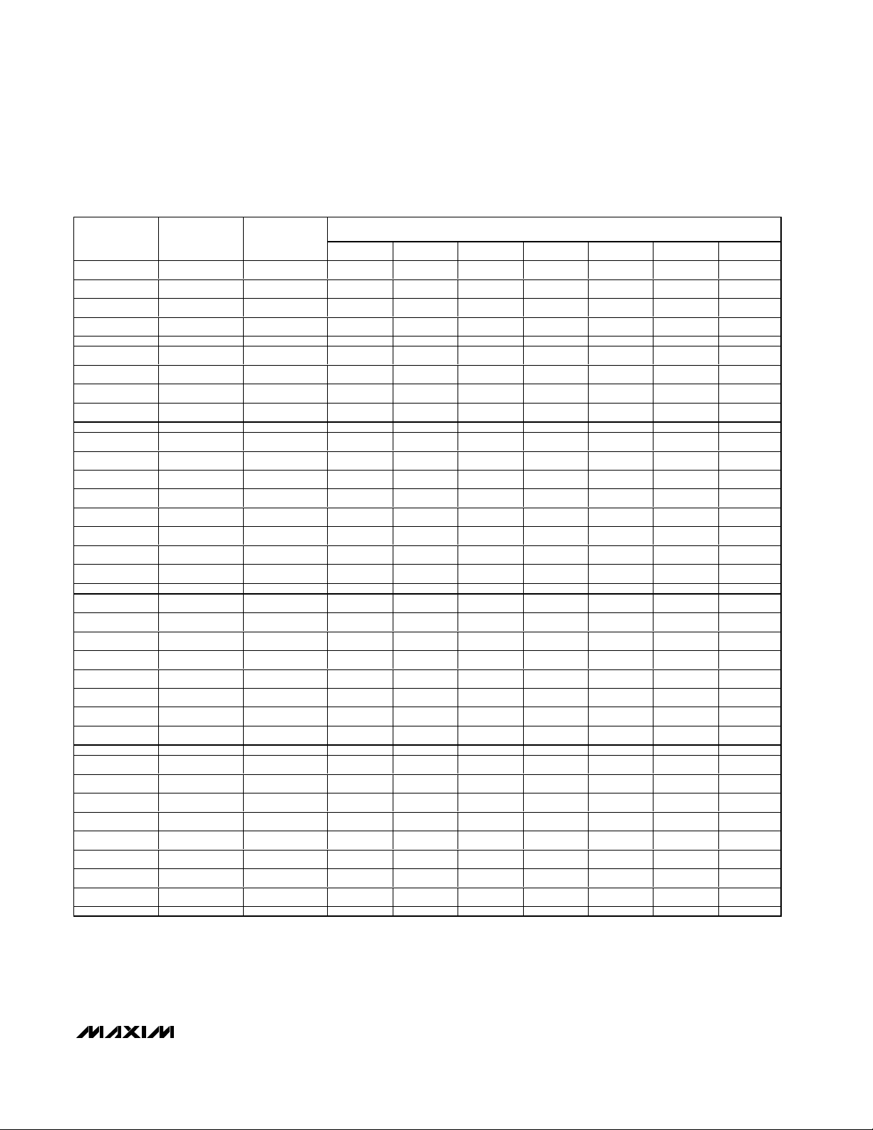
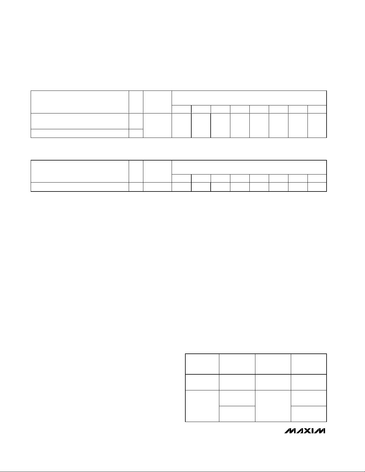
ELECTRICAL CHARACTERISTICS
(Typical Operating Circuit, V+ = 2V to 3.6V, TA= T
MIN
to T
MAX
, unless otherwise noted. Typical values are at V+ = 3.3V, TA = +25°C.)
(Note 1)
Operating Supply Voltage V+ 2 3.6 V
Output Load External Supply
Voltage
Standby Current
(Interface Idle, PWM Disabled)
Supply Current
(Interface Idle, PWM Enabled)
Supply Current
(Interface Running, PWM
Disabled)
Supply Current
(Interface Running, PWM
Enabled)
Input High Voltage
SDA, SCL, AD0, AD1, AD2,
P0–P7
PARAMETER SYMBOL CONDITIONS MIN TYP MAX UNITS
V
EXT
S C L and S D A at V + ; other
I
d i g i tal i np uts at V + or GN D ;
+
P WM i ntensi ty contr ol d i sab l ed
S C L and S D A at V + ; other
I
d i g i tal i np uts at V + or GN D ;
+
P WM i ntensi ty contr ol enab l ed
f
I
inputs at V+ or GND; PWM
+
intensity control disabled
f
I
inputs at V+ or GND; PWM
+
intensity control enabled
V
IH
= 400kHz; other digital
SCL
= 400kHz; other digital
SCL
TA = +25°C 1.2 2.3
TA = -40°C to +85°C 2.6
T
= T
= T
= T
= T
MIN
MIN
MIN
MIN
to T
to T
to T
to T
MAX
MAX
MAX
MAX
A
TA = +25°C 7 12.1
TA = -40°C to +85°C 13.5
T
A
TA = +25°C4076
TA = -40°C to +85°C78
T
A
TA = +25°C 51 110
TA = -40°C to +85°C 117
T
A
0 5.5 V
0.7 ✕
V+
3.3
14.4
80
122
µA
µA
µA
µA
V
Input Low Voltage
SDA, SCL, AD0, AD1, AD2,
P0–P7
Input Leakage Current
SDA, SCL, AD0, AD1, AD2,
P0–P7
Input Capacitance
SDA, SCL, AD0, AD1, AD2,
P0–P7
V
IL
I
, IIL0 ≤ input voltage ≤ 5.5V -0.2 +0.2 µA
IH
0.3 ✕
V+
8pF
V
Page 3
MAX7315
8-Port I/O Expander with LED Intensity
Control and Interrupt
_______________________________________________________________________________________ 3
ELECTRICAL CHARACTERISTICS (continued)
(Typical Operating Circuit, V+ = 2V to 3.6V, TA= T
MIN
to T
MAX
, unless otherwise noted. Typical values are at V+ = 3.3V, TA= + 25°C.)
(Note 1)
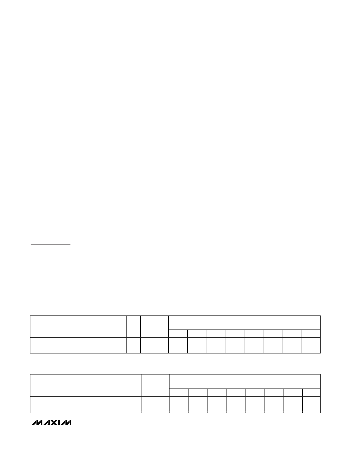
TIMING CHARACTERISTICS
(Typical Operating Circuit, V+ = 2V to 3.6V, TA= T
MIN
to T
MAX
, unless otherwise noted. Typical values are at V+ = 3.3V, TA = +25°C.)
(Note 1)
Output Low Voltage
P0–P7, INT/O8
PARAMETER SYMBOL CONDITIONS MIN TYP MAX UNITS
OL
V+ = 2.5V, I
V
V+ = 3.3V, I
Output Low-Voltage SDA V
PWM Clock Frequency f
OLSDAISINK
PWM
= 20mA
SINK
= 20mA
SINK
= 20mA
SINK
= 6mA 0.4 V
PARAMETER SYMBOL CONDITIONS MIN TYP MAX UNITS
Serial Clock Frequency f
Bus Free Time Between a STOP and a START
Condition
Hold Time, Repeated START Condition t
Repeated START Condition Setup Time t
STOP Condition Setup Time t
Data Hold Time t
Data Setup Time t
SCL Clock Low Period t
SCL Clock High Period t
Rise Time of Both SDA and SCL Signals, Receiving t
Fall Time of Both SDA and SCL Signals, Receiving t
Fall Time of SDA Transmitting t
Pulse Width of Spike Suppressed t
Capacitive Load for Each Bus Line C
SCL
t
BUF
HD, STA
SU, STA
SU, STO
HD, DAT
SU, DAT
LOW
HIGH
F.TX
(Note 2) 0.9 µs
(Notes 3, 4)
R
(Notes 3, 4)
F
(Notes 3, 5)
(Note 6) 50 ns
SP
(Note 3) 400 pF
b
TA = +25°C 0.15 0.25
TA = -40°C to +85°C 0.29V+ = 2V, I
T
= T
MIN
to T
MAX
A
0.31
TA = +25°C 0.13 0.22
TA = -40°C to +85°C 0.25
= T
MIN
to T
MAX
T
A
0.27
TA = +25°C 0.12 0.22
TA = -40°C to +85°C 0.23
= T
MIN
to T
MAX
T
A
0.25
32 kHz
400 kHz
1.3 µs
0.6 µs
0.6 µs
0.6 µs
180 ns
1.3 µs
0.7 µs
200 +
0.1C
200 +
0.1C
200 +
0.1C
300 ns
b
300 ns
b
250 ns
b
V
Page 4
MAX7315
8-Port I/O Expander with LED Intensity
Control and Interrupt
4 _______________________________________________________________________________________
TIMING CHARACTERISTICS (continued)
(Typical Operating Circuit, V+ = 2V to 3.6V, TA= T
MIN
to T
MAX
, unless otherwise noted. Typical values are at V+ = 3.3V, TA = +25°C.)
(Note 1)
Note 1: All parameters tested at TA= +25°C. Specifications over temperature are guaranteed by design.
Note 2: A master device must provide a hold time of at least 300ns for the SDA signal (referred to V
IL
of the SCL signal) to bridge
the undefined region of SCL’s falling edge.
Note 3: Guaranteed by design.
Note 4: C
b
= total capacitance of one bus line in pF. tRand tFmeasured between 0.3 x VDDand 0.7 x VDD.
Note 5: I
SINK
≤ 6mA. Cb= total capacitance of one bus line in pF. tRand tFmeasured between 0.3 x VDDand 0.7 x VDD.
Note 6: Input filters on the SDA and SCL inputs suppress noise spikes less than 50ns.
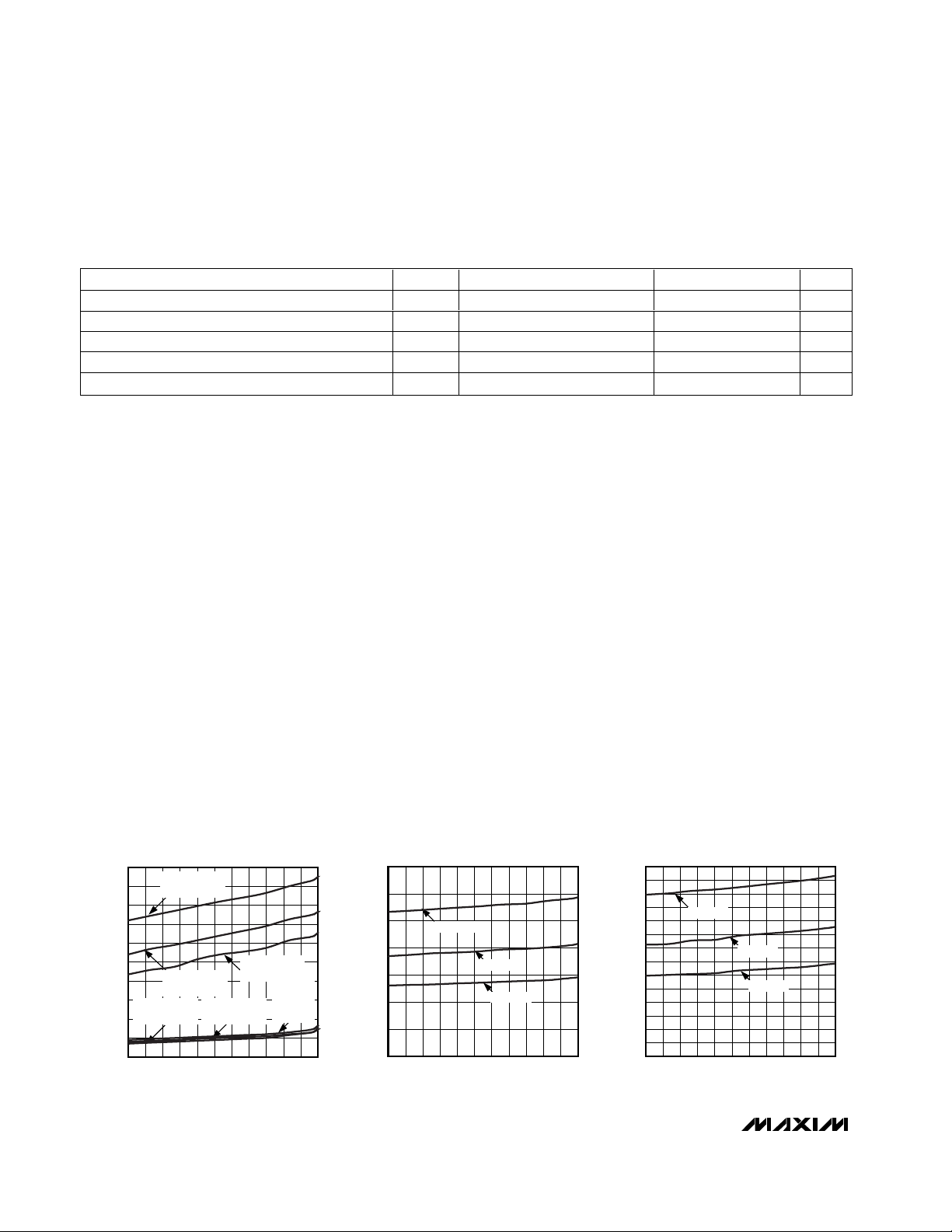
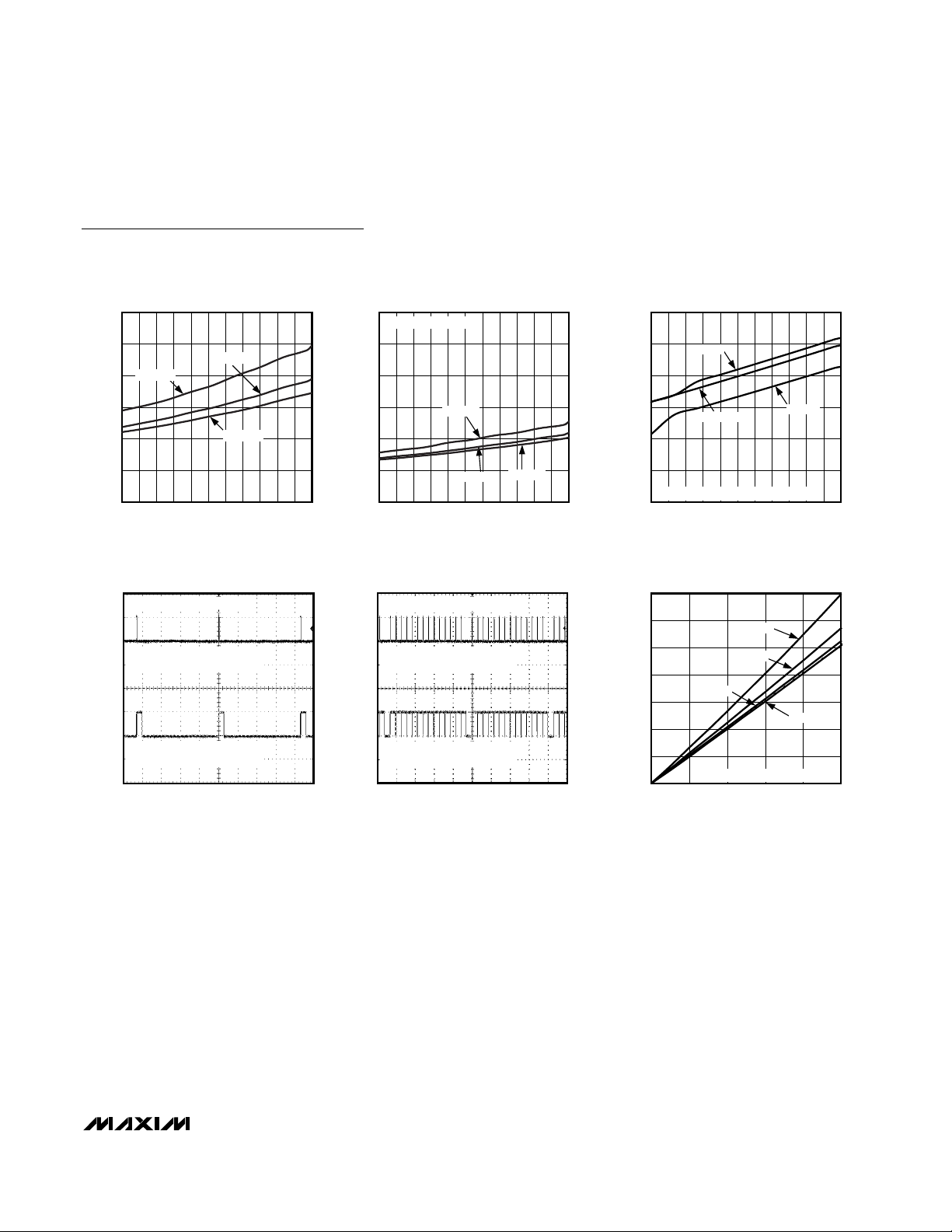
STANDBY CURRENT vs. TEMPERATURE
MAX7315 toc01
TEMPERATURE (°C)
STANDBY CURRENT (µA)
1109565 80-10 5 20 35 50-25
1
2
3
4
5
6
7
8
9
10
0
-40 125
V+ = 3.6V
PWM ENABLED
V+ = 2.7V
PWM ENABLED
V+ = 2V
PWM DISABLED
V+ = 2.7V
PWM DISABLED
V+ = 3.6V
PWM
DISABLED
V+ = 2V
PWM ENABLED
SUPPLY CURRENT vs. TEMPERATURE
(PWM DISABLED; f
SCL
= 400kHz)
MAX7315 toc02
TEMPERATURE (°C)
SUPPLY CURRENT (µA)
1109565 80-10 5 20 35 50-25
10
20
30
40
50
60
70
0
-40 125
V+ = 3.6V
V+ = 2.7V
V+ = 2V
5
10
15
20
25
30
35
40
45
50
55
60
65
70
0
SUPPLY CURRENT vs. TEMPERATURE
(PWM ENABLED; f
SCL
= 400kHz)
MAX7315 toc03
TEMPERATURE (°C)
SUPPLY CURRENT (µA)
1109565 80-10 5 20 35 50-25-40 125
V+ = 3.6V
V+ = 2.7V
V+ = 2V
__________________________________________Typical Operating Characteristics
(TA = +25°C, unless otherwise noted.)
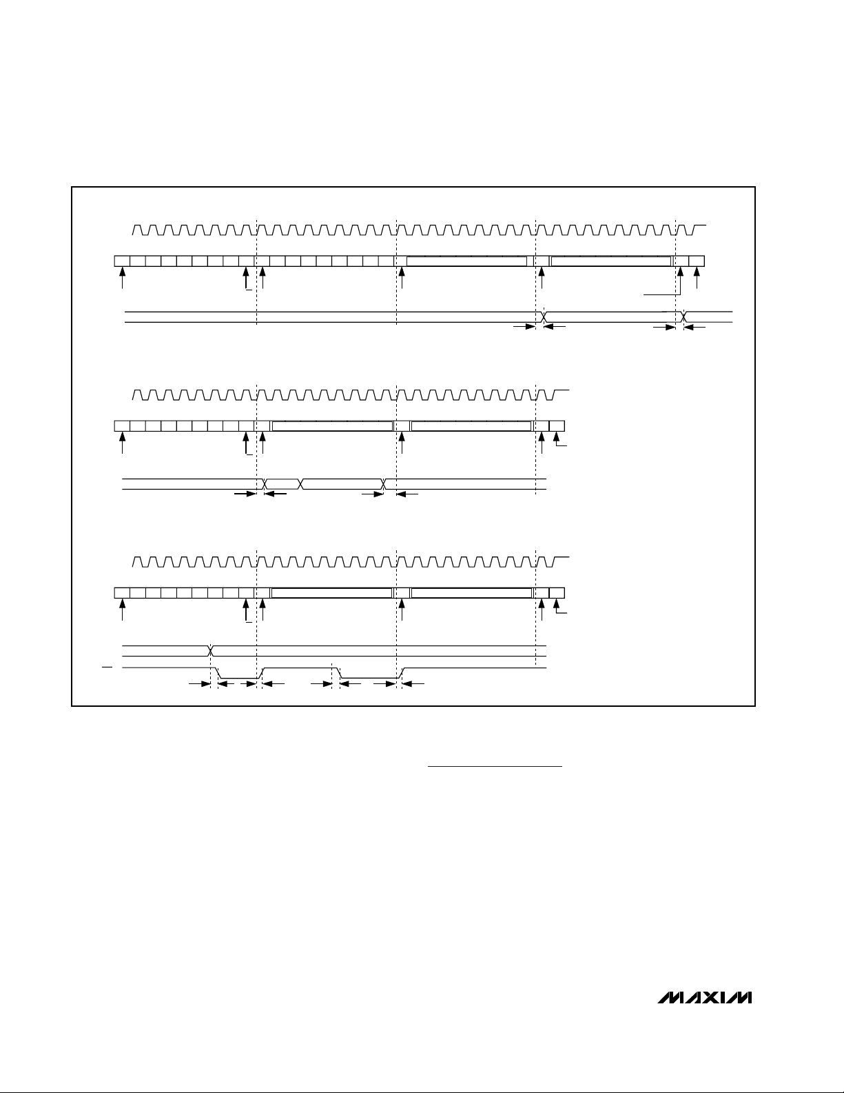
PARAMETER SYMBOL CONDITIONS MIN TYP MAX UNITS
Interrupt Valid t
Interrupt Reset t
Output Data Valid t
Input Data Step Time t
Input Data Hold Time t
Figure 10 6.5 µs
IV
Figure 10 1 µs
IR
Figure 10 5 µs
DV
Figure 10 100 ns
DS
Figure 10 1 µs
DH
Page 5
MAX7315
8-Port I/O Expander with LED Intensity
Control and Interrupt
_______________________________________________________________________________________ 5
1
2
Typical Operating Characteristics (continued)
(TA = +25°C, unless otherwise noted.)
PORT OUTPUT LOW VOLTAGE WITH 50mA
LOAD CURRENT vs. TEMPERATURE
0.6
(V)
0.5
OL
V+ = 2V
0.4
0.3
0.2
0.1
PORT OUTPUT LOW VOLTAGE V
0
SCOPE SHOT OF 2 OUTPUT PORTS
MASTER INTENSITY SET TO 1/15
OUTPUT 1 INDIVIDUAL INTENSITY
SET TO 1/16
OUTPUT 2 INDIVIDUAL INTENSITY
SET TO 15/16
V+ = 2.7V
V+ = 3.6V
1109565 80-10 5 20 35 50-25-40 125
TEMPERATURE (°C)
MAX7315 toc07
2ms/div
PORT OUTPUT LOW VOLTAGE WITH 20mA
LOAD CURRENT vs. TEMPERATURE
0.6
ALL OUTPUTS LOADED
(V)
0.5
MAX7315 toc04
OL
0.4
0.3
0.2
0.1
PORT OUTPUT LOW VOLTAGE V
0
-40 125
SCOPE SHOT OF 2 OUTPUT PORTS
MASTER INTENSITY SET TO 14/15
OUTPUT
2V/div
OUTPUT 1 INDIVIDUAL INTENSITY
SET TO 1/16
OUTPUT
2V/div
OUTPUT 2 INDIVIDUAL INTENSITY
SET TO 14/15
V+ = 2V
V+ = 2.7V
TEMPERATURE (°C)
2ms/div
V+ = 3.6V
MAX7315 toc08
1109580655035205-10-25
MAX7315 toc05
OUTPUT 1,
2V/div
OUTPUT 2,
2V/div
1.050
1.025
1.000
0.975
0.950
PWM CLOCK FREQUENCY
0.925
0.900
0.35
0.30
0.25
0.20
(V)
OL
V
0.15
0.10
0.05
PWM CLOCK FREQUENCY
vs. TEMPERATURE
V+ = 3.6V
V+ = 2.7V
NORMALIZED TO V+ = 3.3V, TA = +25°C
-40 125
TEMPERATURE (°C)
SINK CURRENT vs. V
V+ = 2V
V+ = 2.7V
V+ = 3.3V
0
0
ONLY ONE OUTPUT LOADED
SINK CURRENT (mA)
MAX7315 toc06
V+ = 2V
1109580655035205-10-25
OL
MAX7315 toc09
V+ = 3.6V
5040302010
Page 6
MAX7315
Functional Overview
The MAX7315 is a general-purpose input/output (GPIO)
peripheral that provides eight I/O ports, P0–P7, controlled through an I2C-compatible serial interface. A 9th
output-only port, INT/O8, can be configured as an interrupt output or as a general-purpose output port. All output ports sink loads up to 50mA connected to external
supplies up to 5.5V, independent of the MAX7315’s
supply voltage. The MAX7315 is rated for a ground current of 190mA, allowing all nine outputs to sink 20mA at
the same time. Figure 1 shows the output structure of
the MAX7315. The ports default to inputs on power-up.
Port Inputs and Transition Detection
An input ports register reflects the incoming logic levels
of the port pins, regardless of whether the pin is
defined as an input or an output. Reading the input
8-Port I/O Expander with LED Intensity
Control and Interrupt
6 _______________________________________________________________________________________
Pin Description
Figure 1. Simplified Schematic of I/O Ports
PIN
QSOP/TSSOP QFN
1, 2, 3 15, 16, 1
4–7, 9–12 2–5, 7–10 P0–P7 Input/Output Ports. P0–P7 are open-drain I/Os rated at 5.5V, 50mA.
8 6 GND Ground. Do not sink more than 190mA into the GND pin.
13 11 INT/O8
14 12 SCL I2C-Compatible Serial Clock Input
15 13 SDA I2C-Compatible Serial Data I/O
16 14 V+
— PAD Exposed pad Exposed Pad on Package Underside. Connect to GND.
DATA FROM
SHIFT REGISTER
DATA FROM
SHIFT REGISTER
WRITE
CONFIGURATION
PULSE
WRITE PULSE
NAME FUNCTION
AD0, AD1,
AD2
Address Inputs. Sets device slave address. Connect to either GND, V+,
SCL, or SDA to give 64 logic combinations. See Table 1.
Output Port. Open-drain output rated at 7.0V, 50mA. Configurable as
interrupt output or general-purpose output.
Positive Supply Voltage. Bypass V+ to GND with a 0.047µF ceramic
capacitor
CONFIGURATION
REGISTER
D
Q
FF
C
Q
K
OUTPUT
PORT
REGISTER
D
FF
C
K
Q
Q
OUTPUT PORT
REGISTER DATA
I/O PIN
Q2
READ PULSE
INPUT PORT
REGISTER
D
Q
FF
C
Q
K
GND
INPUT PORT
REGISTER DATA
TO INT
Page 7
ports register latches the current-input logic level of the
affected eight ports. Transition detection allows all
ports configured as inputs to be monitored for changes
in their logic status. The action of reading the input
ports register samples the corresponding 8 port bits’
input condition. This sample is continuously compared
with the actual input conditions. A detected change in
input condition causes the INT/O8 interrupt output to go
low, if configured as an interrupt output. The interrupt is
cleared either automatically if the changed input
returns to its original state, or when the input ports register is read.
The INT/O8 pin can be configured as either an interrupt
output or as a 9th output port with the same static or
blink controls as the other eight ports (Table 4).
Port Output Control and LED Blinking
The blink phase 0 register sets the output logic levels of
the eight ports P0–P7 (Table 8). This register controls
the port outputs if the blink function is disabled. A
duplicate register, the blink phase 1 register, is also
used if the blink function is enabled (Table 9). In blink
mode, the port outputs can be flipped between using
the blink phase 0 register and the blink phase 1 register using software control (the blink flip flag in the configuration register) (Table 4).
PWM Intensity Control
The MAX7315 includes an internal oscillator, nominally
32kHz, to generate PWM timing for LED intensity control. PWM intensity control can be enabled on an output-by-output basis, allowing the MAX7315 to provide
any mix of PWM LED drives and glitch-free logic outputs (Table 10). PWM can be disabled entirely, in
which case all output ports are static and the MAX7315
operating current is lowest because the internal oscillator is turned off.
PWM intensity control uses a 4-bit master control and 4
bits of individual control per output (Tables 13, 14). The
4-bit master control provides 16 levels of overall intensity control, which applies to all PWM-enabled output
ports. The master control sets the maximum pulse
width from 1/15 to 15/15 of the PWM time period. The
individual settings comprise a 4-bit number further
reducing the duty cycle to be from 1/16 to 15/16 of the
time window set by the master control.
For applications requiring the same PWM setting for all
output ports, a single global PWM control can be used
instead of all the individual controls to simplify the control software and provide 240 steps of intensity control
(Tables 10 and 13).
Standby Mode
When the serial interface is idle and the PWM intensity
control is unused, the MAX7315 automatically enters
standby mode. If the PWM intensity control is used, the
operating current is slightly higher because the internal
PWM oscillator is running. When the serial interface is
active, the operating current also increases because
the MAX7315, like all I2C slaves, has to monitor every
transmission.
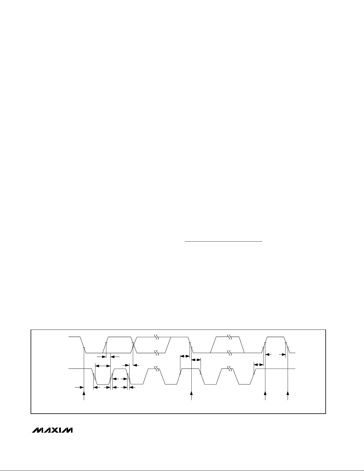
Serial Interface
Serial Addressing
The MAX7315 operates as a slave that sends and
receives data through an I2C-compatible 2-wire interface. The interface uses a serial data line (SDA) and a
serial clock line (SCL) to achieve bidirectional communication between master(s) and slave(s). A master (typically a microcontroller) initiates all data transfers to and
from the MAX7315 and generates the SCL clock that
synchronizes the data transfer (Figure 2).
The MAX7315 SDA line operates as both an input and
an open-drain output. A pullup resistor, typically 4.7kΩ,
is required on SDA. The MAX7315 SCL line operates
MAX7315
8-Port I/O Expander with LED Intensity
Control and Interrupt
_______________________________________________________________________________________ 7
Figure 2. 2-Wire Serial Interface Timing Details
SDA
t
SU,DAT
t
LOW
SCL
t
HD,STA
START CONDITION
t
HIGH
t
t
R
F
t
HD,DAT
t
SU,STA
REPEATED START CONDITION
t
HD,STA
t
SU,STO
STOP
CONDITION
t
BUF
START
CONDITION
Page 8
MAX7315
only as an input. A pullup resistor, typically 4.7kΩ, is
required on SCL if there are multiple masters on the 2wire interface, or if the master in a single-master system
has an open-drain SCL output.
Each transmission consists of a START condition
(Figure 3) sent by a master, followed by the MAX7315
7-bit slave address plus R/W bit, a register address
byte, one or more data bytes, and finally a STOP condition (Figure 3).
Start and Stop Conditions
Both SCL and SDA remain high when the interface is
not busy. A master signals the beginning of a transmission with a START (S) condition by transitioning SDA
from high to low while SCL is high. When the master
has finished communicating with the slave, it issues a
STOP (P) condition by transitioning SDA from low to
high while SCL is high. The bus is then free for another
transmission (Figure 3).
Bit Transfer
One data bit is transferred during each clock pulse.
The data on SDA must remain stable while SCL is high
(Figure 4).
Acknowledge
The acknowledge bit is a clocked 9th bit that the recipient uses to handshake receipt of each byte of data
(Figure 5). Thus, each byte transferred effectively
requires 9 bits. The master generates the 9th clock
pulse, and the recipient pulls down SDA during the
acknowledge clock pulse so the SDA line is stable low
during the high period of the clock pulse. When the
master is transmitting to the MAX7315, the device generates the acknowledge bit because the MAX7315 is
the recipient. When the MAX7315 is transmitting to the
master, the master generates the acknowledge bit
because the master is the recipient.
Slave Address
The MAX7315 has a 7-bit long slave address (Figure 6).
The eighth bit following the 7-bit slave address is the
R/W bit. The R/W bit is low for a write command, high
for a read command.
The slave address bits A6 through A0 are selected by
the address inputs AD0, AD1, and AD2. These pins can
be connected to GND, V+, SDA, or SCL. The MAX7315
has 64 possible slave addresses (Table 1) and, therefore, a maximum of 64 MAX7315 devices can be controlled independently from the same interface.
Message Format for Writing the MAX7315
A write to the MAX7315 comprises the transmission of
the MAX7315’s slave address with the R/W bit set to
zero, followed by at least 1 byte of information. The first
byte of information is the command byte. The command
byte determines which register of the MAX7315 is to be
written to by the next byte, if received (Table 2). If a
STOP condition is detected after the command byte is
received, then the MAX7315 takes no further action
beyond storing the command byte.
8-Port I/O Expander with LED Intensity
Control and Interrupt
8 _______________________________________________________________________________________
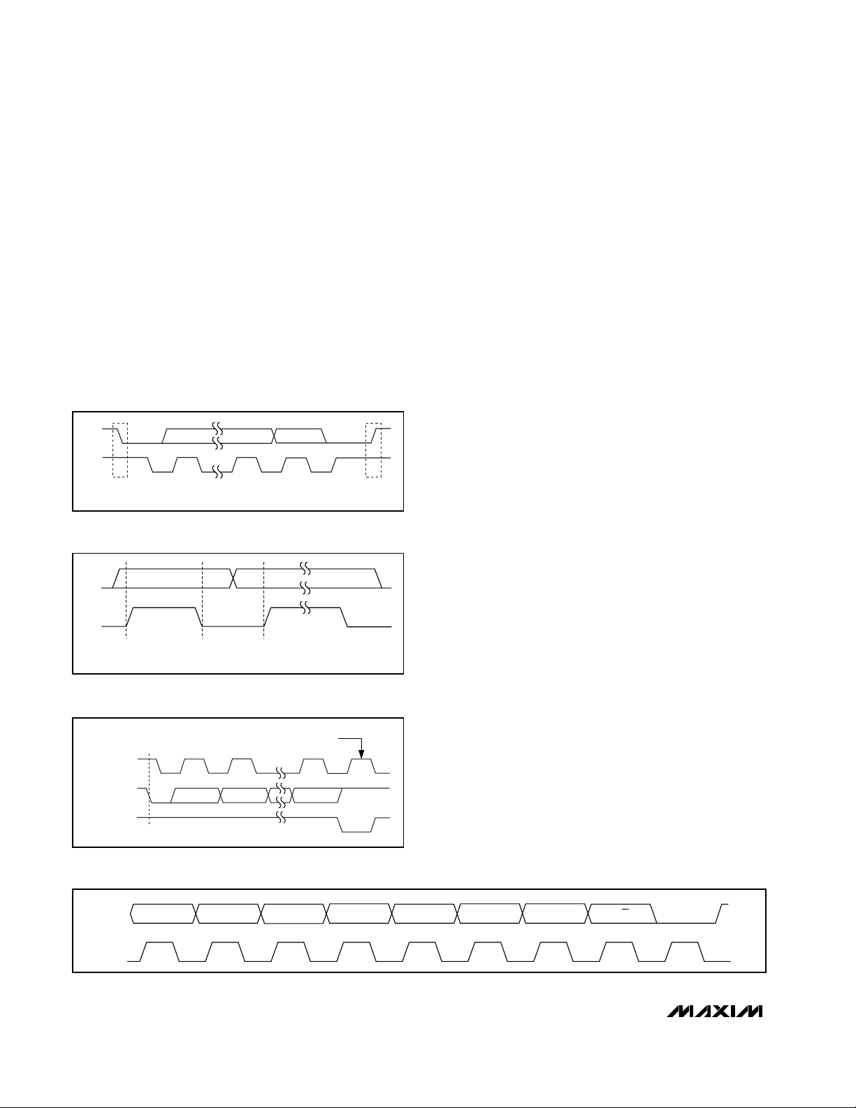
Figure 3. Start and Stop Conditions
Figure 4. Bit Transfer
Figure 5. Acknowledge
Figure 6. Slave Address
SDA
SCL
SP
START
CONDITION
SDA
SCL
DATA LINE STABLE;
DATA VALID
START
CONDITION
SCL
SDA BY
TRANSMITTER
SDA BY
RECEIVER
S
CHANGE OF DATA
ALLOWED
CLOCK PULSE
FOR ACKNOWLEDGE
12 89
STOP
CONDITION
SDA
MSB
SCL
A5
LSB
ACKA4 A1A6 A3 A0A2 R/W
Page 9
MAX7315
8-Port I/O Expander with LED Intensity
Control and Interrupt
_______________________________________________________________________________________ 9
Table 1. MAX7315 I2C Slave Address Map
PIN AD2 PIN AD1 PIN AD0
A6 A5 A4 A3 A2 A1 A0
GND SCL GND0010000
GND SCL V+ 0010001
GNDSDAGND0010010
GNDSDA V+ 0010011
V+ SCL GND0010100
V+ SCL V+ 0010101
V+ SDAGND0010110
V+ SDA V+ 0010111
GND SCL SCL0011000
GND SCL SDA 0011001
GNDSDA SCL 0011010
GNDSDA SDA0011011
V+ SCL SCL 0011100
V+ SCL SDA0011101
V+ SDA SCL 0011110
V+ SDA SDA0011111
GNDGNDGND0100000
GNDGND V+ 0100001
GND V+ GND0100010
GND V+ V+ 0100011
V+ GNDGND0100100
V+ GND V+ 0100101
V+ V+ GND0100110
V+ V+ V+ 0100111
DEVICE ADDRESS
GNDGND SCL 0101000
GNDGNDSDA0101001
GND V+ SCL 0101010
GND V+ SDA0101011
V+ GND SCL 0101100
V+ GNDSDA0101101
V+ V+ SCL 0101110
V+ V+ SDA0101111
Page 10

MAX7315
8-Port I/O Expander with LED Intensity
Control and Interrupt
10 ______________________________________________________________________________________
Table 1. MAX7315 I2C Slave Address Map (continued)
PIN AD2 PIN AD1 PIN AD0
SCL SCL GND1010000
SCL SCL V+ 1010001
SCL SDA GND1010010
SCL SDA V+ 1010011
SDA SCL GND1010100
SDA SCL V+ 1010101
SDA SDA GND1010110
SDA SDA V+ 1010111
SCL SCL SCL1011000
SCL SCL SDA 1011001
SCL SDA SCL 1011010
SCL SDA SDA1011011
SDA SCL SCL 1011100
SDA SCL SDA 1011101
SDA SDA SCL 1011110
SDA SDA SDA 1011111
SCL GNDGND1100000
SCL GND V+ 1100001
SCL V+ GND1100010
SCL V+ V+ 1100011
SDAGNDGND1100100
SDAGND V+ 1100101
SDA V+ GND1100110
SDA V+ V+ 1100111
A6 A5 A4 A3 A2 A1 A0
DEVICE ADDRESS
SCL GND SCL 1101000
SCL GNDSDA1101001
SCL V+ SCL 1101010
SCL V+ SDA1101011
SDAGND SCL 1101100
SDAGNDSDA1101101
SDA V+ SCL 1101110
SDA V+ SDA 1101111
Page 11

Any bytes received after the command byte are data
bytes. The first data byte goes into the internal register
of the MAX7315 selected by the command byte (Figure
8). If multiple data bytes are transmitted before a STOP
condition is detected, these bytes are generally stored
in subsequent MAX7315 internal registers because the
command byte address autoincrements (Table 2). A
diagram of a write to the output ports registers (blink
phase 0 register or blink phase 1 register) is given in
Figure 10.
Message Format for Reading
The MAX7315 is read using the MAX7315’s internally
stored command byte as an address pointer the same
way the stored command byte is used as an address
pointer for a write. The pointer autoincrements after
each data byte is read using the same rules as for a
write (Table 2). Thus, a read is initiated by first configuring the MAX7315’s command byte by performing a
write (Figure 7). The master can now read n consecu-
tive bytes from the MAX7315 with the first data byte
being read from the register addressed by the initialized command byte. When performing read-after-write
verification, remember to reset the command byte’s
address because the stored command byte address
has been autoincremented after the write (Table 2). A
diagram of a read from the input ports register is shown
in Figure 10 reflecting the states of the ports.
Operation with Multiple Masters
If the MAX7315 is operated on a 2-wire interface with
multiple masters, a master reading the MAX7315 should
use a repeated start between the write, which sets the
MAX7315’s address pointer, and the read(s) that takes
the data from the location(s) (Table 2). This is because it
is possible for master 2 to take over the bus after master
1 has set up the MAX7315’s address pointer but before
master 1 has read the data. If master 2 subsequently
changes the MAX7315’s address pointer, then master
1’s delayed read can be from an unexpected location.
MAX7315
8-Port I/O Expander with LED Intensity
Control and Interrupt
______________________________________________________________________________________ 11
Figure 8. Command and Single Data Byte Received
Figure 9. n Data Bytes Received
Figure 7. Command Byte Received
COMMAND BYTE IS STORED ON RECEIPT OF
ACKNOWLEDGE FROM MAX7315
SAA
HOW COMMAND BYTE AND DATA BYTE MAP INTO
SAAAP0SLAVE ADDRESS COMMAND BYTE DATA BYTE
HOW COMMAND BYTE AND DATA BYTE MAP INTO
SAAAP0SLAVE ADDRESS COMMAND BYTE DATA BYTE
MAX7315'S REGISTERS
ACKNOWLEDGE FROM MAX7315
R/W
MAX7315'S REGISTERS
ACKNOWLEDGE FROM MAX7315
R/W
STOP CONDITION
0SLAVE ADDRESS COMMAND BYTE
R/W
ACKNOWLEDGE FROM MAX7315 ACKNOWLEDGE FROM MAX7315
D15 D14 D13 D12 D11 D10 D9 D8 D1 D0D3 D2D5 D4D7 D6
ACKNOWLEDGE FROM MAX7315 ACKNOWLEDGE FROM MAX7315
D15 D14 D13 D12 D11 D10 D9 D8 D1 D0D3 D2D5 D4D7 D6
D15 D14 D13 D12 D11 D10 D9 D8
ACKNOWLEDGE FROM MAX7315
1
AUTOINCREMENT MEMORY ADDRESS
AUTOINCREMENT MEMORY ADDRESS
BYTE
N
BYTES
P
Page 12
MAX7315
Command Address Autoincrementing
The command address stored in the MAX7315 circulates around grouped register functions after each data
byte is written or read (Table 2).
Device Reset
If a device reset input is needed, consider the
MAX7316. The MAX7316 includes a RST input, which
clears any transaction to or from the MAX7316 on the
serial interface and configures the internal registers to
the same state as a power-up reset.
Detailed Description
Initial Power-Up
On power-up all control registers are reset and the
MAX7315 enters standby mode (Table 3). Power-up
status makes all ports into inputs and disables both the
PWM oscillator and blink functionality.
Configuration Register
The configuration register is used to configure the PWM
intensity mode, interrupt, and blink behavior, operate
the INT/O8 output, and read back the interrupt status
(Table 4).
8-Port I/O Expander with LED Intensity
Control and Interrupt
12 ______________________________________________________________________________________
Figure 10. Read, Write, and Interrupt Timing Diagrams
WRITE TO OUTPUT PORTS REGISTERS (BLINK PHASE 0 REGISTERS/BLINK PHASE 1 REGISTERS)
SCL
123456789
SLAVE ADDRESS
SDA
SA6A5A4A3A2A1A00 A0000000
COMMAND BYTE
1A A AP
MSB LSBDATA1
MSB LSBDATA2
START CONDITION
P7–P0
READ FROM INPUT PORTS REGISTERS
SCL
123456789
SLAVE ADDRESS
SDA
SA6A5A4A3A2A1A0 1 A
START CONDITION
P7–P0
INTERRUPT VALID/RESET
SCL
123456789
SLAVE ADDRESS
SDA
S A6A5A4A3A2A1A0 1 A
START CONDITION
P7–P0
INT
DATA 1
ACKNOWLEDGE FROM SLAVE
R/W
COMMAND BYTE
MSB LSBDATA1
ACKNOWLEDGE FROM SLAVE
R/W
DATA 1 DATA 2 D ATA3 DATA 4
R/W
t
IV
t
DH
COMMAND BYTE
MSB LSBDATA2 MSB LSBDATA4
ACKNOWLEDGE FROM SLAVE
DATA 2
t
t
IV
IR
ACKNOWLEDGE FROM SLAVE ACKNOWLEDGE FROM SLAVE STOP
ANA
MSB LSBDATA4
ACKNOWLEDGE FROM MASTER
t
DS
ANA
ACKNOWLEDGE FROM MASTER
DATA 3
t
IR
DATA1 VALID
t
DV
P
STOP CONDITION
NO ACKNOWLEDGE FROM
MASTER
P
STOP CONDITION
NO ACKNOWLEDGE FROM
MASTER
CONDITION
t
DV
DATA2 VALID
Page 13
Ports Configuration
The 8 I/O ports P0 through P7 can be configured to any
combination of inputs and outputs using the ports configuration register (Table 5). The INT/O8 output can
also be configured as an extra general-purpose output
using the configuration register (Table 4).
Input Ports
The input ports register is read only (Table 6). It reflect
the incoming logic levels of the ports, regardless of
whether the port is defined as an input or an output by
the ports configuration register. Reading the input ports
register latches the current-input logic level of the
affected eight ports. A write to the input ports register is
ignored.
Transition Detection
All ports configured as inputs are always monitored for
changes in their logic status. The action of reading the
input ports register or writing to the configuration register samples the corresponding 8 port bits’ input condition (Tables 4, 6). This sample is continuously
compared with the actual input conditions. A detected
change in input condition causes an interrupt condition.
The interrupt is cleared either automatically if the
changed input returns to its original state, or when the
input ports register is read, updating the compared
data (Figure 10). Randomly changing a port from an
output to an input may cause a false interrupt to occur
if the state of the input does not match the content of
the input ports register. The interrupt status is available
as the interrupt flag INT in the configuration register
(Table 4).
The input status of all ports is sampled immediately
after power-up as part of the MAX7315’s internal initial-
ization, so if all the ports are pulled to valid logic levels
at that time an interrupt does not occur at power-up.
INT
/O8 Output
The INT/O8 output pin can be configured as either the
INT output that reflects the interrupt flag logic state or as
a general-purpose output O8. When used as a generalpurpose output, the INT/O8 pin has the same blink and
PWM intensity control capabilities as the other ports.
Set the interrupt enable I bit in the configuration register
to configure INT/O8 as the INT output (Table 4). Clear
interrupt enable to configure INT/O8 as the O8. O8
logic state is set by the 2 bits O1 and O0 in the configuration register. O8 follows the rules for blinking selected
by the blink enable flag E in the configuration register.
If blinking is disabled, then interrupt output control O0
alone sets the logic state of the INT/O8 pin. If blinking is
enabled, then both interrupt output controls O0 and O1
set the logic state of the INT/O8 pin according to the
blink phase. PWM intensity control for O8 is set by the 4
global intensity bits in the master, O8 intensity register
(Table 13).
Blink Mode
In blink mode, the output ports can be flipped between
using either the blink phase 0 register or the blink phase
1 register. Flip control is by software control (the blink flip
flag B in the configuration register) (Table 4). If hardware
flip control is needed, consider the MAX7316, which
includes a BLINK input, as well as software control.
The blink function can be used for LED effects by programming different display patterns in the two sets of
MAX7315
8-Port I/O Expander with LED Intensity
Control and Interrupt
______________________________________________________________________________________ 13
Table 2. Register Address Map
REGISTER
Read input ports 0x00 0x00 (no change)
Blink phase 0 outputs 0x01 0x01 (no change)
Ports configuration 0x03 0x03 (no change)
Blink phase 1 outputs 0x09 0x09 (no change)
Master, O8 intensity 0x0E 0x0E (no change)
Configuration 0x0F 0x0F (no change)
Outputs intensity P1, P0 0x10 0x11
Outputs intensity P3, P2 0x11 0x12
Outputs intensity P5, P4 0x12 0x13
Outputs intensity P7, P6 0x13 0x10
ADDRESS CODE
(HEX)
AUTOINCREMENT
ADDRESS
Page 14

MAX7315
8-Port I/O Expander with LED Intensity
Control and Interrupt
14 ______________________________________________________________________________________
Table 3. Power-Up Configuration
Table 4. Configuration Register
REGISTER DATA
REGISTER
ADDRESS
CODE
(HEX)
D7 D6 D5 D4 D3 D2 D1 D0
CONFIGURATION
R/W
INTERRUPT
STATUS
—
INTERRUPT
OUTPUT
CONTROL
AS GPO
INTERRUPT
ENABLE
GLOBAL
INTENSITY
BLINK FLIP
BLINK
ENABLE
Write device configuration
X
Read-back device configuration
O
O0 I G B E
Disable blink
XXXXXXX0
Enable blink
XXXXXXX1
XXXXXX01
Flip blink register (see text)
XXXXXX11
Disable global intensity control—intensity
is set by registers 0x10–0x13 for ports P0
through P7 when configured as outputs,
and by D3–D7 of register 0x0E for INT/O8
when INT/O8 pin is configured as an
output port
XXXXX0 XX
Enable global intensity control—intensity
for all ports configured as outputs is set
by D3–D0 of register 0x0E
0x0F
XXXXX1 XX
REGISTER FUNCTION POWER-UP CONDITION
Blink phase 0 outputs P7–P0 High-impedance outputs 0x01 1 1 1 1 1 1 1 1
Ports configuration P7–P0 Ports P7–P0 are inputs 0x03 1 1 1 1 1 1 1 1
Blink phase 1 outputs P7–P0 High-impedance outputs 0x09 1 1 1 1 1 1 1 1
Master, O8 intensity
Configuration
Outputs intensity P1, P0 P1, P0 are static logic outputs 0x10 1 1 1 1 1 1 1 1
Outputs Intensity P3, P2 P3, P2 are static logic outputs 0x11 1 1 1 1 1 1 1 1
Outputs intensity P5, P4 P5, P4 are static logic outputs 0x12 1 1 1 1 1 1 1 1
Outputs intensity P7, P6 P7, P6 are static logic outputs 0x13 1 1 1 1 1 1 1 1
PWM oscillator is disabled;
O8 is static logic output
INT/O8 is interrupt output;
blink is disabled;
global intensity is enabled
ADDRESS
CODE
(HEX)
0x0E 0 0 0 0 1 1 1 1
0x0F 0 0 0 0 1 1 0 0
D7 D6 D5 D4 D3 D2 D1 D0
REGISTER DATA
0
1
—
—
—
—
—
—
INT
O1
Page 15
output port registers, and using the software or hardware controls to flip between the patterns.
If the blink phase 1 register is written with 0xFF, then
the BLINK input can be used as a hardware disable to,
for example, instantly turn off an LED pattern programmed into the blink phase 0 register. This technique can be further extended by driving the BLINK
input with a PWM signal to modulate the LED current to
provide fading effects.
The blink mode is enabled by setting the blink enable
flag E in the configuration register (Table 4). When blink
mode is enabled, the state of the blink flip flag sets the
phase, and the output ports are set by either the blink
phase 0 register or the blink phase 1 register (Table 7).
The blink mode is disabled by clearing the blink enable
flag E in the configuration register (Table 4). When blink
mode is disabled, the blink phase 0 register alone controls the output ports.
Blink Phase Registers
When the blink function is disabled, the blink phase 0
register sets the logic levels of the 8 ports (P0 through
P7) when configured as outputs (Table 8). A duplicate
register called the blink phase 1 register is also used if
the blink function is enabled (Table 9). A logic high sets
the appropriate output port high impedance, while a
logic low makes the port go low.
MAX7315
8-Port I/O Expander with LED Intensity
Control and Interrupt
______________________________________________________________________________________ 15
Table 4. Configuration register (continued)
REGISTER DATA
REGISTER
ADDRESS
CODE
(HEX)
D7 D6 D5 D4 D3 D2 D1 D0
CONFIGURATION
R/W
INTERRUPT
STATUS
—
INTERRUPT
OUTPUT
CONTROL
AS GPO
INTERRUPT
ENABLE
GLOBAL
INTENSITY
BLINK FLIP
BLINK
ENABLE
X
Disable data change interrupt—INT/O8
output is controlled by the O0 and O1 bits
O
O0 I G B E
Enable data change interrupt—INT/O8
output is controlled by port input data
change
XXXX1 XXX
INT/O8 output is low (blink is disabled)
XXX00XX0
INT/O8 output is high impedance (blink is
disabled)
XXX10XX0
INT/O8 outp ut i s l ow d ur i ng b l i nk p hase 0
XXX00XX1
INT/O8 output is high impedance during
blink phase 0
XXX10XX1
INT/O8 outp ut i s l ow d ur i ng b l i nk p hase 1
XX0 X 0 XX1
INT/O8 output is high impedance during
blink phase 1
XX1 X 0 XX1
Read-back data change interrupt status
—data change is not detected, and
INT/O8 output is high when interrupt
enable (I bit) is set
0 0XXXXXX
Read-back data change interrupt status
—data change is detected, and INT/O8
output is low when interrupt enable (I bit)
is set
0x0F
1 0XXXXXX
— INT
—
—
—
—
—
—
—
O1
1
1
Page 16
MAX7315
Reading a blink phase register reads the value stored
in the register, not the actual port condition. The port
output itself may or may not be at a valid logic level,
depending on the external load connected.
The 9th output, O8, is controlled through 2 bits in the
configuration register, which provide the same static or
blink control as the other 8 output ports.
PWM Intensity Control
The MAX7315 includes an internal oscillator, nominally
32kHz, to generate PWM timing for LED intensity control or other applications such as PWM trim DACs. PWM
can be disabled entirely for all the outputs. In this case,
all outputs are static and the MAX7315 operating current is lowest because the internal PWM oscillator is
turned off.
The MAX7315 can be configured to provide any combination of PWM outputs and glitch-free logic outputs.
Each PWM output has an individual 4-bit intensity control (Table 14). When all outputs are to be used with the
same PWM setting, the outputs can be controlled
together instead using the global intensity control
(Table 13). Table 10 shows how to set up the MAX7315
to suit a particular application.
PWM Timing
The PWM control uses a 240-step PWM period, divided
into 15 master intensity timeslots. Each master intensity
timeslot is divided further into 16 PWM cycles (Figure 11).
The master intensity operates as a gate, allowing the individual output settings to be enabled from 1 to 15 timeslots
per PWM period (Figures 12, 13, 14) (Table 13).
Each output’s individual 4-bit intensity control only
operates during the number of timeslots gated by the
master intensity. The individual controls provide 16
intensity settings from 1/16 through 16/16 (Table 14).
Figures 15, 16, and 17 show examples of individual
intensity control settings. The highest value an individual or global setting can be set to is 16/16. This setting
forces the output to ignore the master control, and follow the logic level set by the appropriate blink phase
register bit. The output becomes a glitch-free static output with no PWM.
Using PWM Intensity Controls with Blink Disabled
When blink is disabled (Table 7), the blink phase 0 register specifies each output’s logic level during the PWM
on-time (Table 8). The effect of setting an output’s blink
phase 0 register bit to 0 or 1 is shown in Table 11. With
its output bit set to zero, an LED can be controlled with
16 intensity settings from 1/16th duty through fully on,
but cannot be turned fully off using the PWM intensity
control. With its output bit set to 1, an LED can be controlled with 16 intensity settings from fully off through
15/16th duty.
8-Port I/O Expander with LED Intensity
Control and Interrupt
16 ______________________________________________________________________________________
Table 5. Ports Configuration Register
Table 6. Input Ports Register
Table 7. Blink Controls
REGISTER R/W
Ports configuration
(1 = input, 0 = output)
Read-back ports configuration 1
ADDRESS
0
REGISTER R/W
Read input ports 1 0x00 IP7 IP6 IP5 IP4 IP3 IP2 IP1 IP0
ADDRESS
CODE
(HEX)
0x03 OP7 OP6 OP5 OP4 OP3 OP2 OP1 OP0
CODE
(HEX)
D7 D6 D5 D4 D3 D2 D1 D0
D7 D6 D5 D4 D3 D2 D1 D0
REGISTER DATA
REGISTER DATA
BLINK
ENABLE
FLAG E
0 X Disabled
1
BLINK
FLIP
FLAG B
0
1
BLINK
FUNCTION
Enabled
OUTPUT
REGISTERS
USED
Blink phase 0
register
Blink phase 0
register
Blink phase 1
register
Page 17
Using PWM Intensity Controls with Blink Enabled
When blink is enabled (Table 7), the blink phase 0 register and blink phase 1 register specify each output’s logic
level during the PWM on-time during the respective blink
phases (Tables 8 and 9). The effect of setting an output’s
blink phase X register bit to 0 or 1 is shown in Table 12.
LEDs can be flipped between either directly on and off,
or between a variety of high/low PWM intensities.
Global/O8 Intensity Control
The 4 bits used for output O8’s PWM individual intensity
setting also double as the global intensity control
(Table 13). Global intensity simplifies the PWM settings
when the application requires them all to be the same,
such as for backlight applications, by replacing the 9
individual settings with 1 setting. Global intensity is
enabled with the global intensity flag G in the configuration register (Table 4). When global PWM control is
used, the 4 bits of master intensity and 4 bits of O8
intensity effectively combine to provide an 8 bit, 240step intensity control applying to all outputs.
It is not possible to apply global PWM control to a subset of the ports, and use the others as logic outputs. To
mix static logic outputs and PWM outputs, individual
PWM control must be selected (Table 10).
Applications Information
Output Level Translation
The open-drain output architecture allows the ports to
level translate the outputs to higher or lower voltages
than the MAX7315 supply. An external pullup resistor
can be used on any output to convert the high-impedance logic-high condition to a positive voltage level.
The resistor can be connected to any voltage up to
5.5V. For interfacing CMOS inputs, a pullup resistor
value of 220kΩ is a good starting point. Use a lower
resistance to improve noise immunity, in applications
where power consumption is less critical, or where a
faster rise time is needed for a given capacitive load.
Compatibility with PCA9534 and
PCA9554(A)
The MAX7315 is pin compatible and software compatible
with PCA9534, and its variants PCA9554 and
PCA9554A. However, some PCA9534 and PCA9554(A)
functions are not implemented in the MAX7315, and the
MAX7315's PWM and blink functionality is not supported
in the PCA9534 and PCA9554(A). Software compatibility
is clearly not 100%, but the MAX7315 was designed so
the subset (omitted) features default to the same powerup behavior as the PCA9534 and PCA9554(A), and the
superset features do not use existing registers in a different way. In practice, many applications can use the
MAX7315 as a drop-in replacement for the PCA9534 or
PCA9554(A) with no software change.
Driving LED Loads
When driving LEDs, a resistor in series with the LED
must be used to limit the LED current to no more than
50mA. Choose the resistor value according to the following formula:
R
LED
= (V
SUPPLY
- V
LED
- VOL) / I
LED
where:
R
LED
is the resistance of the resistor in series with the
LED (Ω).
V
SUPPLY
is the supply voltage used to drive the LED (V).
V
LED
is the forward voltage of the LED (V).
MAX7315
8-Port I/O Expander with LED Intensity
Control and Interrupt
______________________________________________________________________________________ 17
Table 8. Blink Phase 0 Register
Table 9. Blink Phase 1 Register
REGISTER R/W
Write outputs phase 0 0
Read-back outputs phase 0 1
REGISTER R/W
Write outputs phase 1 0
Read-back outputs phase 1 1
ADDRESS
CODE
(HEX)
0x01 OP7 OP6 OP5 OP4 OP3 OP2 OP1 OP0
ADDRESS
CODE
(HEX)
0x09 OP7 OP6 OP5 OP4 OP3 OP2 OP1 OP0
D7 D6 D5 D4 D3 D2 D1 D0
D7 D6 D5 D4 D3 D2 D1 D0
REGISTER DATA
REGISTER DATA
Page 18

MAX7315
8-Port I/O Expander with LED Intensity
Control and Interrupt
18 ______________________________________________________________________________________
Table 10. PWM Application Scenarios
Figure 11. PWM Timing
Figure 12. Master Set to 1/15
Figure 14. Master Set to 15/15
Figure 13. Master Set to 14/15
APPLICATION RECOMMENDED CONFIGURATION
All outputs static without PWM
A mix of static and PWM outputs, with PWM
outputs using different PWM settings
A mix of static and PWM outputs, with PWM
outputs all using the same PWM setting
All outputs PWM using the same PWM
setting
1 2 3 4 5 6 7 8 9 10 11 12 13 14 15 14 15 1 2
Set the master, O8 intensity register 0x0E to any value from 0x00 to 0x0F.
The global intensity G bit in the configuration register is don't care.
The output intensity registers 0x10 through 0x13 are don't care.
Set the master, O8 intensity register 0x0E to any value from 0x10 to 0xFF.
Clear global intensity G bit to 0 in the configuration register to disable global intensity
control.
For the static outputs, set the output intensity value to 0xF.
For the PWM outputs, set the output intensity value in the range 0x0 to 0xE.
As above. Global intensity control cannot be used with a mix of static and PWM
outputs, so write the individual intensity registers with the same PWM value.
Set the master, O8 intensity register 0x0E to any value from 0x10 to 0xFF.
Set global intensity G bit to 1 in the configuration register to enable global intensity
control.
The master, O8 intensity register 0x0E is the only intensity register used.
The output intensity registers 0x10 through 0x13 are don't care.
ONE PWM PERIOD IS 240 CYCLES OF THE 32kHz PWM
OSCILLATOR. A PWM PERIOD CONTAINS 15 MASTER
INTENSITY TIMESLOTS
1 2 3 4 5 6 7 8 9 10 11 12 13 14 15 16 15 16 1 2
EACH MASTER INTENSITY
TIMESLOT CONTAINS 16
PWM CYCLES
1 2 3 4 5 6 7 8 9 10 11 12 13 14 15 14 15 2 1
.
.
1 2 3 4 5 6 7 8 9 10 11 12 13 14 15 14 15 2 1
.
.
1 2 3 4 5 6 7 8 9 10 11 12 13 14 15 14 15 2 1
.
Page 19

MAX7315
8-Port I/O Expander with LED Intensity
Control and Interrupt
______________________________________________________________________________________ 19
Figure 16. Individual (or Global) Set to 15/16
Figure 15. Individual (or Global) Set to 1/16
Figure 17. Individual (or Global) Set to 16/16
Table 11. PWM Intensity Settings (Blink Disabled)
MASTER INTENSITY TIMESLOT
1 2 3 4 5 6 7 8 9 10 11 12 13 14 15 16
MASTER INTENSITY TIMESLOT
1 2 3 4 5 6 7 8 9 10 11 12 13 14 15 16
MASTER INTENSITY TIMESLOT CONTROL IS IGNORED
1 2 3 4 5 6 7 8 9 10 11 12 13 14 15 16 1 2 3 4 5 6 7 8 9 10 11 12 13 14 15 16
OUTPUT
(OR
GLOBAL)
INTENSITY
SETTING
0x0 1/16 15/16 Lowest PWM intensity 15/16 1/16 Highest PWM intensity
0x1 2/16 14/16 14/16 2/16
0x2 3/16 13/16 13/16 3/16
0x3 4/16 12/16 12/16 4/16
0x4 5/16 11/16 11/16 5/16
0x5 6/16 10/16 10/16 6/16
0x6 7/16 9/16 9/16 7/16
0x7 8/16 8/16 8/16 8/16
0x8 9/16 7/16 7/16 9/16
0x9 10/16 6/16 6/16 10/16
0xA 11/16 5/16 5/16 11/16
0xB 12/16 4/16 4/16 12/16
0xC 13/16 3/16 3/16 13/16
0xD 14/16 2/16
0xE 15/16 1/16 Highest PWM intensity 1/16 15/16 Lowest PWM intensity
0xF Static low Static low
PWM DUTY CYCLE
OUTPUT BLINK PHASE 0
REGISTER BIT = 0
LOW TIME HIGH TIME
LED BEHAVIOR WHEN
OUTPUT BLINK PHASE 0
REGISTER BIT = 0
(LED IS ON WHEN
OUTPUT IS LOW)
Increasing PWM intensity
Full intensity, no PWM
(LED on continuously)
1 2 3 4 5 6 7 8 9 10 11 12 13 14 15 16
1 2 3 4 5 6 7 8 9 10 11 12 13 14 15 16
NEXT MASTER INTENSITY TIMESLOT
NEXT MASTER INTENSITY TIMESLOT
PWM DUTY CYCLE
OUTPUT BLINK PHASE 0
REGISTER BIT = 1
LOW TIME HIGH TIME
2/16 14/16
Static high
impedance
Static high
impedance
LED BEHAVIOR WHEN
OUTPUT BLINK PHASE 0
REGISTER BIT = 1
(LED IS ON WHEN
OUTPUT IS LOW)
LED off continuously
Increasing PWM intensity
Page 20
MAX7315
VOLis the output low voltage of the MAX7313 when
sinking I
LED
(V).
I
LED
is the desired operating current of the LED (A).
For example, to operate a 2.2V red LED at 14mA from a
5V supply, R
LED
= (5 - 2.2 - 0.25) / 0.014 = 182Ω.
Driving Load Currents Higher than 50mA
The MAX7315 can be used to drive loads drawing more
than 50mA, like relays and high-current white LEDs, by
paralleling outputs. Use at least one output per 50mA of
load current; for example, a 5V 330mW relay draws
66mA and needs two paralleled outputs to drive it.
Ensure that the paralleled outputs chosen are controlled
by the same blink phase register, i.e., select outputs
from the P0 through P7 range. This way, the paralleled
outputs are turned on and off together. Do not use output O8 as part of a load-sharing design. O8 cannot be
switched at the same time as any of the other outputs
because it is controlled by a different register.
The MAX7315 must be protected from the negative
voltage transient generated when switching off induc-
tive loads, such as relays, by connecting a reversebiased diode across the inductive load (Figure 18). The
peak current through the diode is the inductive load’s
operating current.
Power-Supply Considerations
The MAX7315 operates with a power-supply voltage of
2V to 3.6V. Bypass the power supply to GND with at
least 0.047µF as close to the device as possible.
Chip Information
TRANSISTOR COUNT: 17,611
PROCESS: BiCMOS
8-Port I/O Expander with LED Intensity
Control and Interrupt
20 ______________________________________________________________________________________
Table 12. PWM Intensity Settings (Blink Enabled)
OUTPUT
(OR
GLOBAL)
INTENSITY
SETTING
0x0 1/16 15/16 15/16 1/16
0x1 2/16 14/16 14/16 2/16
0x2 3/16 13/16 13/16 3/16
0x3 4/16 12/16 12/16 4/16
0x4 5/16 11/16 11/16 5/16
0x5 6/16 10/16 10/16 6/16
0x6 7/16 9/16 9/16 7/16
0x7 8/16 8/16 8/16 8/16 Output is half intensity during both blink phases
0x8 9/16 7/16 7/16 9/16
0x9 10/16 6/16 6/16 10/16
0xA 11/16 5/16 5/16 11/16
0xB 12/16 4/16 4/16 12/16
0xC 13/16 3/16 3/16 13/16
0xD 14/16 2/16 2/16 14/16
0xE 15/16 1/16 1/16 15/16
0xF Static low Static low
PWM DUTY CYCLE
OUTPUT BLINK
PHASE X
REGISTER BIT = 0
LOW
TIME
HIGH
TIME
PWM DUTY CYCLE
OUTPUT BLINK
PHASE X
REGISTER BIT = 1
LOW
TIME
Static high
impedance
HIGH
TIME
Static high
impedance
EXAMPLES OF LED BLINK BEHAVIOR
(LED IS ON WHEN OUTPUT IS LOW)
BLINK PHASE 0
REGISTER BIT = 0
BLINK PHASE 1
REGISTER BIT = 1
P hase 0: LE D on at l ow i ntensi ty
P hase 1: LE D on at hi g h i ntensi ty
P hase 0: LE D on at hi g h i ntensi ty
P hase 1: LE D on at l ow i ntensi ty
Phase 0: LED on continuously
Phase 1: LED off continuously
BLINK PHASE 0
REGISTER BIT = 1
BLINK PHASE 1
REGISTER BIT = 0
P hase 0: LE D on at hi g h i ntensi ty
P hase 1: LE D on at l ow i ntensi ty
P hase 0: LE D on at l ow i ntensi ty
P hase 1: LE D on at hi g h i ntensi ty
Phase 0: LED off continuously
Phase 1: LED on continuously
Page 21

MAX7315
8-Port I/O Expander with LED Intensity
Control and Interrupt
______________________________________________________________________________________________________ 21
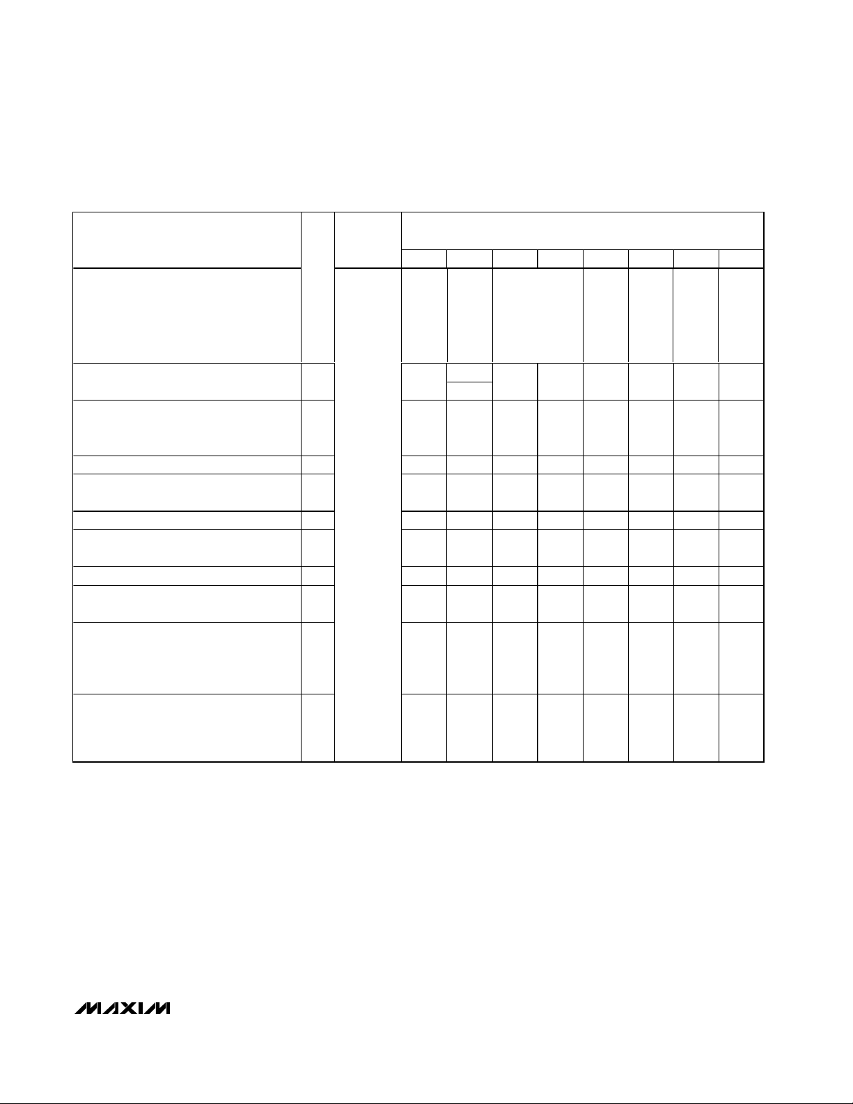
Table 13. Master, O8 Intensity Register
REGISTER
MASTER AND GLOBAL INTENSITY
Write master and global intensity 0
Read back master and global intensity 1
Master intensity duty cycle is 0/15 (off);
internal oscillator is disabled;
all outputs will be static with no PWM
Master intensity duty cycle is 1/15 — 0001————
Master intensity duty cycle is 2/15 — 0010————
Master intensity duty cycle is 3/15 — 0011————
— — ————————
Master intensity duty cycle is 13/15 — 1101————
Master intensity duty cycle is 14/15 — 1110————
Master intensity duty cycle is 15/15 (full) — 1111————
O8 intensity duty cycle is 1/16 — ———— 0000
O8 intensity duty cycle is 2/16 — ———— 0001
O8 intensity duty cycle is 3/16 — ———— 0010
— — ————————
O8 intensity duty cycle is 14/16 — ———— 1101
O8 intensity duty cycle is 15/16 — ———— 1110
O8 intensity duty cycle is 16/16
(static output, no PWM)
ADDRESS
CODE
R/W
(HEX)
— 0000————
0X0E
—
D7 D6 D5 D4 D3 D2 D1 D0
MSB LSB MSB LSB
MASTER INTENSITY O8 INTENSITY
M3 M2 M1 M0 G3 G2 G1 G0
———— 1111
REGISTER DATA
Page 22

MAX7315
8-Port I/O Expander with LED Intensity
Control and Interrupt
22 ______________________________________________________________________________________
Table 14. Output Intensity Registers
REGISTER DATA
REGISTER
ADDRESS
CODE
(HEX)
D7 D6 D5 D4 D3 D2 D1 D0
LSB
OUTPUTS P1, P0 INTENSITY
R/W
OUTPUT P1 INTENSITY OUTPUT P0 INTENSITY
Write output P1, P0 intensity
Read back output P1, P0 intensity
P0I0
Output P1 intensity duty cycle is 1/16
0000————
Output P1 intensity duty cycle is 2/16
0001————
Output P1 intensity duty cycle is 3/16
0010————
—
————————
Output P1 intensity duty cycle is 14/16
1101————
Output P1 intensity duty cycle is 15/16
1110————
Output P1 intensity duty cycle is 16/16
(static logic level, no PWM)
1111————
Output P0 intensity duty cycle is 1/16
———— 0000
Output P0 intensity duty cycle is 2/16
———— 0001
Output P0 intensity duty cycle is 3/16
———— 0010
—
————————
Output P0 intensity duty cycle is 14/16
———— 1101
Output P0 intensity duty cycle is 15/16
———— 1110
Output P0 intensity duty cycle is 16/16
(static logic level, no PWM)
0X10
———— 1111
LSB
OUTPUTS P3, P2 INTENSITY
OUTPUT P3 INTENSITY OUTPUT P2 INTENSITY
Write output P3, P2 intensity
Read back output P3, P2 intensity
0x11
P2I0
LSB
OUTPUTS P5, P4 INTENSITY
OUTPUT P5 INTENSITY OUTPUT P4 INTENSITY
Write output P5, P4 intensity
Read back output P5, P4 intensity
0x12
P4I0
LSB
OUTPUTS P7, P6 INTENSITY
OUTPUT P7 INTENSITY OUTPUT P6 INTENSITY
Write output P7, P6 intensity
Read back output P7, P6 intensity
0x13
P6I0
OUTPUT O8 INTENSITY See the master, O8 intensity register (Table 13).
MSB LSB MSB
0
1
—
—
—
—
—
—
—
—
—
—
—
—
—
—
0
1
P1I3 P1I2 P1I1 P1I0 P0I3 P0I2 P0I1
MSB LSB MSB
P3I3 P3I2 P3I1 P3I0 P2I3 P2I2 P2I1
MSB LSB MSB
0
1
0
1
P5I3 P5I2 P5I1 P5I0 P4I3 P4I2 P4I1
MSB LSB MSB
P7I3 P7I2 P7I1 P7I0 P6I3 P6I2 P6I1
Page 23

MAX7315
8-Port I/O Expander with LED Intensity
Control and Interrupt
______________________________________________________________________________________ 23
Table 15. MAX7311, PCA9535, and PCA9555 Register Compatibility
Figure 18. Diode-Protected Switching Inductive Load
Pin Configurations (continued)
PCA9534,
PCA9554(A)
ADDRESS MAX7313 IMPLEMENTATION
REGISTER
Inputs 0x00 Inputs registers Implemented Same functionality
Outputs 0x01 Blink phase 0 registers Implemented Same functionality
Polarity inversion 0x02
Not implemented; register writes are
ignored; register reads return 0x00
Configuration 0x03 Ports configuration registers Not implemented Same functionality
No registers 0x0B Blink phase 1 registers Not implemented
No register 0x0E Master and global/O8 intensity register Not implemented
No register 0x0F Configuration register Not implemented
No registers 0x10–0x13 Outputs intensity registers Not implemented
2V TO 3.6V
0.047µF
µC
SDA
SCL
5V
V+
SDA
MAX7315
SCL
I/O
INT/O8
AD0
AD1
AD2
GND
P0
P1
BAS16
P2
P3
P4
P5
P6
P7
TOP VIEW
MAX7311, PCA9535,
PCA9555
COMMENTS
IMPLEMENTATION
Implemented;
power-up default is
0x00
If polarity inversion feature
is unused, MAX7313
defaults to correct state
Power-up default disables
the blink and intensity
(PWM) features
AD0
AD1
AD2
P0
P1
P2
P3
GND
1
2
3
MAX7315AEE
4
MAX7315AUE
5
6
7
8
QSOP/TSSOP
16
V+
15
SDA
14
SCL
INT/O8
13
12
P7
P6
11
10
P5
9
P4
Page 24

MAX7315
8-Port I/O Expander with LED Intensity
Control and Interrupt
24 ______________________________________________________________________________________
Package Information
(The package drawing(s) in this data sheet may not reflect the most current specifications. For the latest package outline information,
go to www.maxim-ic.com/packages
.)
QSOP.EPS
PACKAGE OUTLINE, QSOP .150", .025" LEAD PITCH
21-0055
1
E
1
Page 25

MAX7315
8-Port I/O Expander with LED Intensity
Control and Interrupt
______________________________________________________________________________________ 25
Package Information (continued)
(The package drawing(s) in this data sheet may not reflect the most current specifications. For the latest package outline information,
go to www.maxim-ic.com/packages
.)
- A -
C
L
0.10
C
D2
D
D/2
E/2
E
- B -
C
L
0.08
C
A
A2
A1
L
(NE - 1) X e
C
L
e
D2/2
e
b
0.10 M C A B
k
(ND - 1) X e
C
L
e
E2/2
E2
L
L
12x16L QFN THIN.EPS
PROPRIETARY INFORMATION
TITLE:
PACKAGE OUTLINE
12 & 16L, QFN THIN, 3x3x0.8 mm
21-0136
REV.DOCUMENT CONTROL NO.APPROVAL
1
C
2
Page 26

MAX7315
8-Port I/O Expander with LED Intensity
Control and Interrupt
26 ______________________________________________________________________________________
Package Information (continued)
(The package drawing(s) in this data sheet may not reflect the most current specifications. For the latest package outline information,
go to www.maxim-ic.com/packages
.)
EXPOSED PAD VARIATIONS
NOTES:
1. DIMENSIONING & TOLERANCING CONFORM TO ASME Y14.5M-1994.
2. ALL DIMENSIONS ARE IN MILLIMETERS. ANGLES ARE IN DEGREES.
3. N IS THE TOTAL NUMBER OF TERMINALS.
4. THE TERMINAL #1 IDENTIFIER AND TERMINAL NUMBERING CONVENTION SHALL CONFORM TO
JESD 95-1 SPP-012. DETAILS OF TERMINAL #1 IDENTIFIER ARE OPTIONAL, BUT MUST BE LOCATED
WITHIN THE ZONE INDICATED. THE TERMINAL #1 IDENTIFIER MAY BE EITHER A MOLD OR
MARKED FEATURE.
5. DIMENSION b APPLIES TO METALLIZED TERMINAL AND IS MEASURED BETWEEN 0.20 mm AND 0.25 mm
FROM TERMINAL TIP.
6. ND AND NE REFER TO THE NUMBER OF TERMINALS ON EACH D AND E SIDE RESPECTIVELY.
7. DEPOPULATION IS POSSIBLE IN A SYMMETRICAL FASHION.
8. COPLANARITY APPLIES TO THE EXPOSED HEAT SINK SLUG AS WELL AS THE TERMINALS.
9. DRAWING CONFORMS TO JEDEC MO220 REVISION C.
PROPRIETARY INFORMATION
TITLE:
PACKAGE OUTLINE
12 & 16L, QFN THIN, 3x3x0.8 mm
APPROVAL
DOCUMENT CONTROL NO.
21-0136
REV.
2
C
2
Page 27

MAX7315
8-Port I/O Expander with LED Intensity
Control and Interrupt
Maxim cannot assume responsibility for use of any circuitry other than circuitry entirely embodied in a Maxim product. No circuit patent licenses are
implied. Maxim reserves the right to change the circuitry and specifications without notice at any time.
Maxim Integrated Products, 120 San Gabriel Drive, Sunnyvale, CA 94086 408-737-7600 ____________________ 27
© 2003 Maxim Integrated Products Printed USA is a registered trademark of Maxim Integrated Products.
Package Information (continued)
(The package drawing(s) in this data sheet may not reflect the most current specifications. For the latest package outline information,
go to www.maxim-ic.com/packages
.)
TSSOP4.40mm.EPS
 Loading...