

Page 1
General Description
The MAX7311 2-wire-interfaced expander provides 16bit parallel input/output (I/O) port expansion for
SMBus™-compatible and I2C-compatible applications.
The MAX7311 consists of input port registers, output
port registers, polarity inversion registers, configuration
registers, a bus timeout register, and an SMBus/I2Ccompatible serial interface. The system master can
invert the MAX7311 input data by writing to the activehigh polarity inversion register. The system master can
enable or disable bus timeout by writing to the bus
timeout register.
Any of the 16 I/O ports can be configured as an input or
output. A power-on reset (POR) initializes the 16 I/Os
as inputs. Three address select pins configure one of
64 slave ID addresses.
The MAX7311 is available in 24-pin SO, SSOP, TSSOP,
and thin QFN packages and is specified over the -40°C
to +125°C automotive temperature range.
Applications
Servers
RAID Systems
Industrial Control
Medical Equipment
PLCs
Instrumentation and Test Measurement
Features
♦ 400kbps I2C-Compatible Serial Interface
♦ 2V to 5.5V Operation
♦ 5V Overvoltage Tolerant I/Os
♦ 16 I/O Pins that Default to Inputs on Power-Up
♦ Open-Drain Interrupt Output (INT)
♦ Bus Timeout for Lock-Up-Free Operation
♦ 64 Slave ID Addresses Available
♦ Low Standby Current (2.9µA typ)
♦ Polarity Inversion
♦ 4mm
✕ 4mm, 0.8mm Thin QFN Package
♦ -40°C to +125°C Operation
MAX7311
2-Wire-Interfaced 16-Bit I/O Port Expander
with Interrupt
________________________________________________________________ Maxim Integrated Products 1
Ordering Information
19-2747; Rev 0; 1/03
For pricing, delivery, and ordering information, please contact Maxim/Dallas Direct! at
1-888-629-4642, or visit Maxim’s website at www.maxim-ic.com.
SMBus is a trademark of Intel Corp.
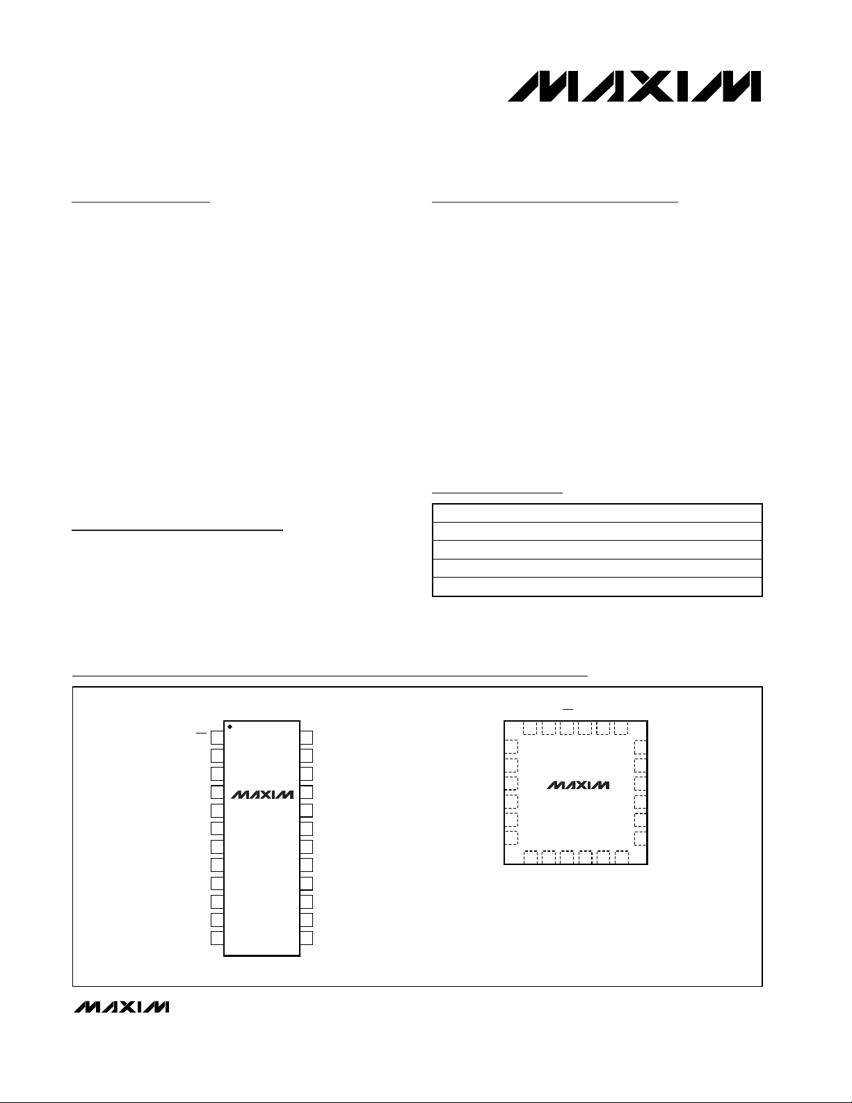
Pin Configurations
+
V
24
SDA
23
SCL
22
AD0I/O0
21
I/O15
20
I/O14
19
I/O13
18
I/O12I/O4
17
16
I/O11
15
I/O10
14
I/O9
13
I/O8GND
AD1
AD2
I/O1
I/O2
I/O3
I/O5
I/O6
I/O7
1
INT
2
3
4
MAX7311
5
6
7
8
9
10
11
12
PART TEMP RANGE PIN-PACKAGE
MAX7311AWG -40°C to +125°C 24 Wide SO
MAX7311AAG -40°C to +125°C 24 SSOP
MAX7311ATG -40°C to +125°C 24 Thin QFN (4mm ✕ 4mm)
MAX7311AUG -40°C to +125°C 24 TSSOP
TOP VIEW
AD2 AD1 V
24 23 22 21 20 19
1
I/O0
2
I/O1
3
I/O2
I/O3
4
I/O4
5
I/O5
6
78 9101112
I/O6 I/O7 GND I/O8 I/O9 I/O10
+
INT
MAX7311
THIN QFN
SDA SCL
18
AD0
17
I/O15
16
I/O14
I/O13
15
I/O12
14
I/O11
13
TSSOP/SSOP/SO
Page 2
MAX7311
2-Wire-Interfaced 16-Bit I/O Port Expander
with Interrupt
2 _______________________________________________________________________________________
ABSOLUTE MAXIMUM RATINGS
DC ELECTRICAL CHARACTERISTICS
(V+= 2V to 5.5V, TA= -40°C to +125°C, unless otherwise noted. Typical values are at V+= 3.3V, TA= +25°C.) (Note 1)
Stresses beyond those listed under “Absolute Maximum Ratings” may cause permanent damage to the device. These are stress ratings only, and functional
operation of the device at these or any other conditions beyond those indicated in the operational sections of the specifications is not implied. Exposure to
absolute maximum rating conditions for extended periods may affect device reliability.
V+to GND ................................................................-0.3V to +6V
I/O0–I/O15 as Inputs ....................................(GND - 0.3V) to +6V
SCL, SDA, AD0, AD1, AD2, INT...................(GND - 0.3V) to +6V
Maximum V
+
Current ......................................................+250mA
Maximum GND Current ...................................................-250mA
DC Input Current on I/O0–I/O15 .......................................±20mA
DC Output Current on I/O0–I/O15 ....................................±80mA
Continuous Power Dissipation (T
A
= +70°C)
24-Pin Wide SO (derate 11.8mW/°C above +70°C) ....941mW
24-Pin SSOP (derate 8.0mW/°C above +70°C) ...........640mW
24-Pin TSSOP (derate 12.2mW/°C above +70°C) .......975mW
24-Pin Thin QFN (derate 20.8mW/°C above +70°C) .1668mW
Operating Temperature Range .........................-40°C to +125°C
Junction Temperature......................................................+150°C
Storage Temperature Range .............................-65°C to +150°C
Lead Temperature (soldering, 10s) .................................+300°C
Supply Voltage V
Power-On Reset Voltage V
SCL, SDA
Input Voltage Low V
Input Voltage High
Low-Level Output Voltage V
Leakage Current I
Input Capacitance 10 pF
I/O_
Input Voltage Low V
Input Voltage High V
Input Leakage Current
Internal Pullup Current TA = -40°C to +85°C, VIO = 0 34 100 µA
Low-Level Output Current I
High Output Current I
AD0, AD1, AD2
Input Voltage Low V
Input Voltage High V
PARAMETER SYM B O L CONDITIONS MIN TYP MAX UNITS
+
+
STBY
POR
IL
V
IH
OL
L
IL
IH
SINK
SOURCE
IL
IH
All I/Os unloaded,
= 400kHz
f
SCL
All I/Os unloaded,
= 0
f
SCL
I
= 6mA 0.4 V
SINK
T
= -40°C to +85°C; includes internal
A
pullup current, V
V+ = 2V, VOL = 0.5V 8.5 17
V+ = 3.3V, VOL = 0.5V 17 32
V+ = 5V, VOL = 0.5V 43
V+ = 3.3V, VOH = 2.4V 29 41
V+ = 5V, VOH = 4.5V 31
= V
IO
V+ = 2V 23 35
V+ = 3.3V 43 60Supply Current I
+
V
= 5.5V 80 120
V+ = 2V 2.3 11
V+ = 3.3V 2.9 12Standby Current I
+
V
= 5.5V 3.8 15.5
+
2 5.5 V
1.4 1.7 V
+
0.3 ✕ V
+
0.7 ✕ V
-1 +1 µA
0.8 V
1.8 V
1µA
+
0.3 ✕ V
0.7 ✕ V
+
µA
µA
V
V
mA
mA
V
V
Page 3
MAX7311
2-Wire-Interfaced 16-Bit I/O Port Expander
with Interrupt
_______________________________________________________________________________________ 3
Note 1: All parameters are 100% production tested at TA= +25°C. Specifications over temperature are guaranteed by design.
Note 2: Minimum SCL clock frequency is limited by the MAX7311 bus timeout feature, which resets the serial bus interface if either
SDA or SCL is held low for a minimum of 25ms. Disable bus timeout feature for DC operation.
Note 3: A master device must internally provide a hold time of at least 300ns for the SDA signal (referred to the V
IL
of the SCL
signal) in order to bridge the undefined region SCL’s falling edge.
Note 4: C
B
= total capacitance of one bus line in pF.
Note 5: The maximum t
F
for the SDA and SCL bus lines is specified at 300ns. The maximum fall time for the SDA output stage tFis
specified at 250ns. This allows series protection resistors to be connected between the SDA and SCL pins and the
SDA/SCL bus lines without exceeding the maximum specified t
F
.
Note 6: Input filters on the SDA and SCL inputs suppress noise spikes less than 50ns.
DC ELECTRICAL CHARACTERISTICS (continued)
(V+= 2V to 5.5V, TA= -40°C to +125°C, unless otherwise noted. Typical values are at V+= 3.3V, TA= +25°C.) (Note 1)
AC ELECTRICAL CHARACTERISTICS
(V+= 2V to 5.5V, TA= -40°C to +125°C, unless otherwise noted.) (Note 1)
Leakage Current -1 +1 µA
Input Capacitance 4pF
INT
Low-Level Output Current I
PARAMETER SYM B O L CONDITIONS MIN TYP MAX UNITS
V
OL
= 0.4V 6 mA
OL
SCL Clock Frequency f
Bus Timeout t
Bus Free Time Between STOP
and START Conditions
Hold Time (Repeated) START
Condition
Repeated START Condition
Setup Time
STOP Condition Setup Time t
Data Hold Time t
Data Setup Time t
SCL Low Period t
SCL High Period t
SDA Fall Time t
Pulse Width of Spike Suppressed t
PORT TIMING
Output Data Valid t
Input Data Setup Time 27 µs
Input Data Hold Time 0µs
INTERRUPT TIMING
Interrupt Valid t
Interrupt Reset t
PARAMETER SYM B O L CONDITIONS MIN TYP MAX UNITS
SCL
TIMEOUT
t
BUF
t
HD,STA
t
SU,STA
SU,STO
HD,DAT
SU,DAT
LOW
HIGH
SP
PV
IR
(Note 2) 400 kHz
29 61 ms
Figure 2 1.3 µs
Figure 2 0.6 µs
Figure 2 0.6 µs
Figure 2 0.6 µs
Figure 2 (Note 3) 0.9 µs
Figure 2 100 ns
Figure 2 1.3 µs
Figure 2 0.7 µs
Figure 2 (Notes 4, 5)
F
(Note 6) 50 ns
Figure 7 3 µs
Figure 9 30.5 µs
IV
Figure 9 2 µs
V+ < 3.3V 500
V+ ≥ 3.3V 250
ns
Page 4
MAX7311
2-Wire-Interfaced 16-Bit I/O Port Expander
with Interrupt
4 _______________________________________________________________________________________
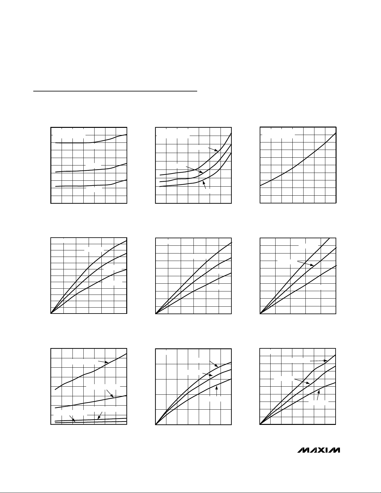
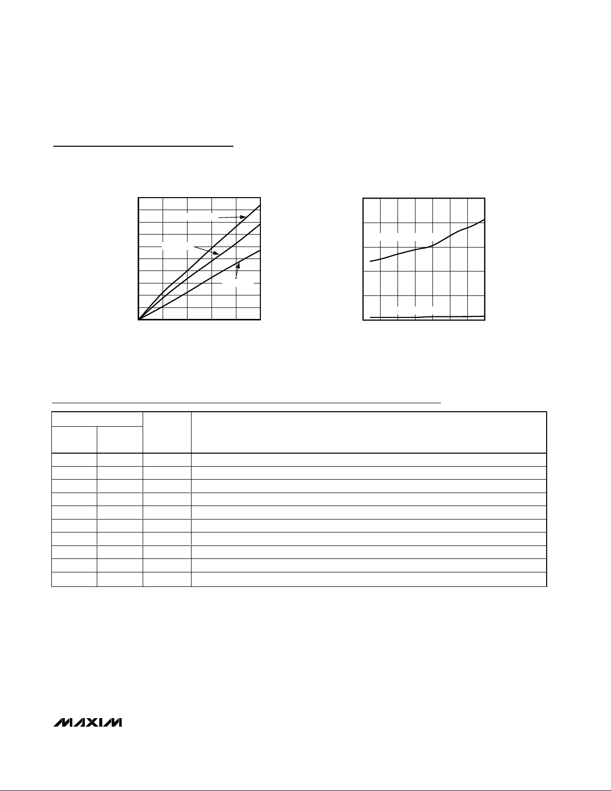
Typical Operating Characteristics
(TA = +25°C, unless otherwise noted.)
SUPPLY CURRENT
vs. TEMPERATURE
MAX7311 toc01
TEMPERATURE (°C)
SUPPLY CURRENT (µA)
1007525 500-25
10
20
30
40
50
60
70
80
90
100
0
-50 125
f
SCL
= 400kHz
ALL I/Os UNLOADED
V+ = 3.3V
V+ = 5V
V+ = 2V
STANDBY SUPPLY CURRENT
vs. TEMPERATURE
MAX7311 toc02
TEMPERATURE (°C)
SUPPLY CURRENT (µA)
1007525 500-25
1
2
3
4
5
6
7
8
9
0
-50 125
SCL = V
+
ALL I/Os UNLOADED
V+ = 3.3V
V+ = 5V
V+ = 2V
SUPPLY CURRENT
vs. SUPPLY VOLTAGE
MAX7311 toc03
SUPPLY VOLTAGE (V)
SUPPLY CURRENT (µA)
5.04.53.5 4.03.02.5
10
20
30
40
50
60
70
80
90
100
0
2.0 5.5
f
SCL
= 400kHz
ALL I/Os UNLOADED
I/O SINK CURRENT
vs. OUTPUT LOW VOLTAGE
MAX7311 toc04
VOL (V)
I
SINK
(mA)
0.50.40.30.20.1
2
4
6
8
10
12
14
16
18
20
22
24
0
0 0.6
V+ = 2V
TA = +125°C
TA = +25°C
TA = -40°C
I/O SINK CURRENT
vs. OUTPUT LOW VOLTAGE
MAX7311 toc05
VOL (V)
I
SINK
(mA)
0.50.40.30.20.1
5
10
15
20
25
30
35
40
45
50
0
0 0.6
V+ = 3.3V
TA = +125°C
TA = -40°C
TA = +25°C
I/O SINK CURRENT
vs. OUTPUT LOW VOLTAGE
MAX7311 toc06
VOL (V)
I
SINK
(mA)
0.40.30.20.1
5
10
15
20
25
30
35
40
45
50
0
0 0.5
V+ = 5V
TA = +125°C
TA = -40°C
TA = +25°C
I/O OUTPUT LOW VOLTAGE
vs. TEMPERATURE
MAX7311 toc07
TEMPERATURE (°C)
V
OL
(mV)
10075-25 0 25 50
50
100
150
200
250
300
350
400
0
-50 125
V+ = 5V, I
SINK
= 10mA
V+ = 2V, I
SINK
= 10mA
V+ = 2V, I
SINK
= 1mA
V+ = 5V, I
SINK
= 1mA
I/O SOURCE CURRENT
vs. OUTPUT HIGH VOLTAGE
MAX7311 toc08
V+ - VOH (V)
I
SOURCE
(mA)
0.60.50.40.30.20.1
5
10
15
20
25
0
0 0.7
V+ = 2V
TA = +125°C
TA = +25°C
TA = -40°C
I/O SOURCE CURRENT
vs. OUTPUT HIGH VOLTAGE
MAX7311 toc09
V+ - VOH (V)
I
SOURCE
(mA)
0.60.50.3 0.40.20.1
5
10
15
20
25
30
35
40
45
50
0
0 0.7
V+ = 3.3V
TA = +125°C
TA = +25°C
TA = -40°C
Page 5
MAX7311
2-Wire-Interfaced 16-Bit I/O Port Expander
with Interrupt
_______________________________________________________________________________________ 5
Pin Description
Typical Operating Characteristics (continued)
(TA = +25°C, unless otherwise noted.)
I/O SOURCE CURRENT
vs. OUTPUT HIGH VOLTAGE
MAX7311 toc10
V+ - VOH (V)
I
SOURCE
(mA)
0.60.50.3 0.40.20.1
5
10
15
20
25
30
35
40
45
50
0
0
V+ = 5V
TA = +125°C
TA = +25°C
TA = -40°C
I/O HIGH VOLTAGE vs. TEMPERATURE
MAX7311 toc11
TEMPERATURE (°C)
V
+
- V
OH
(V)
1007550250-25
100
200
300
400
500
0
-50 125
V+ = 5V, I
SOURCE
= 10mA
V+ = 2V, I
SOURCE
= 10mA
PIN
TSSOP/
SSOP/SO
THIN
QFN
122INT Interrupt Output (Open Drain)
2 23 AD1 Address Input 1
3 24 AD2 Address Input 2
4–11 1–8 I/O0–I/O7 Input/Output Port 1
12 9 GND Supply Ground
13–20 10–17 I/O8–I/O15 Input/Output Port 2
21 18 AD0 Address Input 0
22 19 SCL Serial Clock Line
23 20 SDA Serial Data Line
24 21 V
NAME FUNCTION
+
Supply Voltage. Bypass with a 0.047µF capacitor to GND.
Page 6
MAX7311
Detailed Description
The MAX7311 general-purpose input/output (GPIO)
peripheral provides up to 16 I/O ports, controlled
through an I2C-compatible serial interface. The
MAX7311 consists of input port registers, output port
registers, polarity inversion registers, configuration registers, and a bus-timeout register. Upon power-on, all
I/O lines are set as inputs. Three slave ID address select
pins, AD0, AD1, and AD2, choose one of 64 slave ID
addresses, including the eight addresses supported by
the Phillips PCA9555. Table 1 is the register address
table. Tables 2–6 show detailed register information.
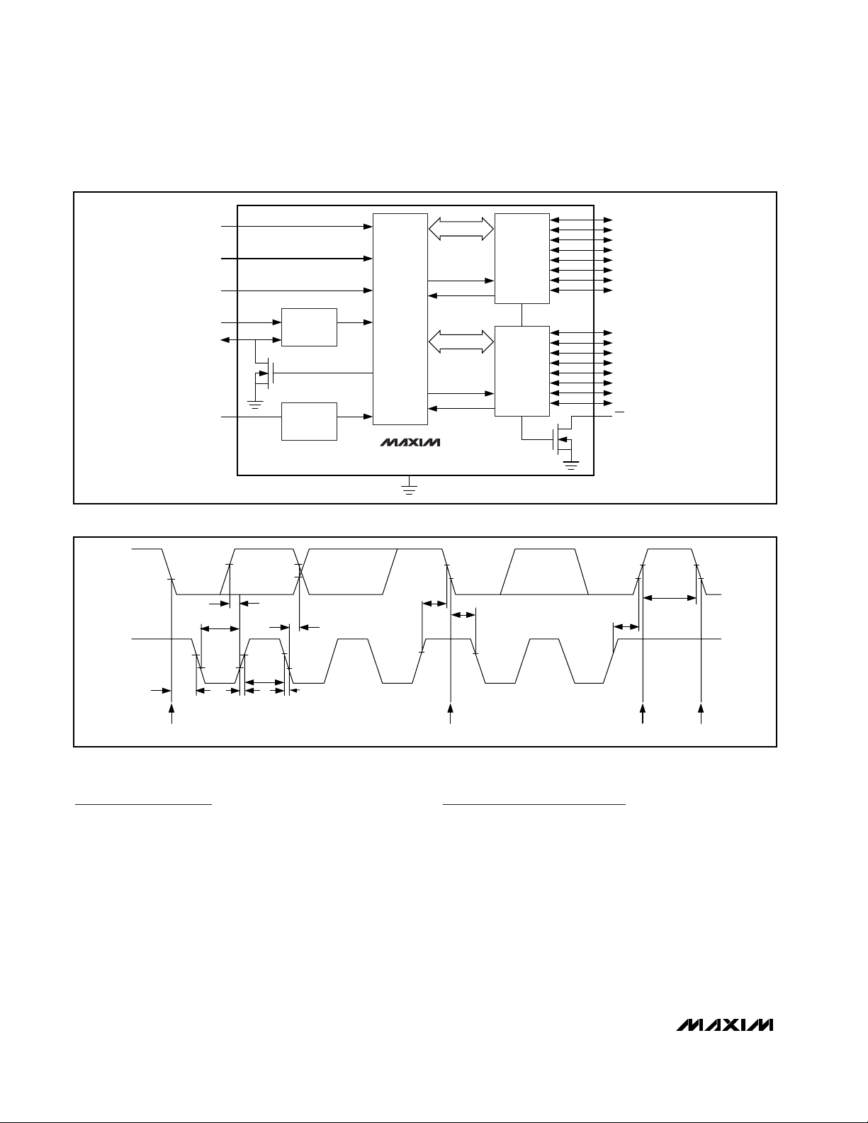
Serial Interface
Serial Addressing
The MAX7311 operates as a slave that sends and
receives data through a 2-wire interface. The interface
uses a serial data line (SDA) and a serial clock line
(SCL) to achieve bidirectional communication between
master(s) and slave(s). A master, typically a microcontroller, initiates all data transfers to and from the
MAX7311, and generates the SCL clock that synchronizes the data transfer (Figure 2).
2-Wire-Interfaced 16-Bit I/O Port Expander
with Interrupt
6 _______________________________________________________________________________________
Figure 1. MAX7311 Block Diagram
Figure 2. 2-Wire Serial Interface Timing Diagram
SDA
SCL
t
SU, STO
I/O0
I/O1
I/O2
I/O3
I/O4
I/O5
I/O6
I/O7
I/O8
I/O9
I/O10
I/O11
I/O12
I/O13
I/O14
I/O15
INT
t
BUF
AD0
AD1
AD2
SCL
SDA
N
+
V
t
LOW
t
SU, DAT
INPUT
FILTER
POWER-ON
RESET
t
HD, DAT
SMBus
CONTROL
MAX7311
t
SU, STA
GND
8 BIT
WRITE PULSE
READ PULSE
8 BIT
WRITE PULSE
READ PULSE
t
HD, STA
INPUT/OUTPUT
PORT 1
INPUT/OUTPUT
PORT 2
t
t
HD, STA
START CONDITION
HIGH
t
R
t
F
REPEATED START CONDITION
START CONDITIONSTOP CONDITION
Page 7

Each transmission consists of a START condition sent by
a master, followed by the MAX7311 7-bit slave address
plus R/W bit, a register address byte, 1 or more data
bytes, and finally a STOP condition (Figure 3).
START and STOP Conditions
Both SCL and SDA remain high when the interface is
not busy. A master signals the beginning of a transmission with a START (S) condition by transitioning SDA
from high to low while SCL is high. When the master
has finished communicating with the slave, it issues a
STOP (P) condition by transitioning SDA from low to
high while SCL is high. The bus is then free for another
transmission (Figure 3).
Bit Transfer
One data bit is transferred during each clock pulse.
The data on SDA must remain stable while SCL is high
(Figure 4).
Acknowledge
The acknowledge bit is a clocked 9th bit, which the
recipient uses as a handshake receipt of each byte of
data (Figure 5). Thus, each byte transferred effectively
requires 9 bits. The master generates the 9th clock
pulse, and the recipient pulls down SDA during the
acknowledge clock pulse, such that the SDA line is stable low during the high period of the clock pulse. When
the master is transmitting to the MAX7311, the
MAX7311
2-Wire-Interfaced 16-Bit I/O Port Expander
with Interrupt
_______________________________________________________________________________________ 7
Figure 3. START and STOP Conditions
Figure 4. Bit Transfer
Figure 5. Acknowledge
SDA
SCL
START CONDITION
SCL
BY TRANSMITTER
SDA
S
START
CONDITION
SDA
SCL
P
STOP
CONDITION
DATA LINE STABLE; DATA VALID
12 89
CHANGE OF DATA ALLOWED
CLOCK PULSE FOR ACKNOWLEDGMENT
S
SDA
BY RECEIVER
Page 8

MAX7311
MAX7311 generates the acknowledge bit since the
MAX7311 is the recipient. When the MAX7311 is transmitting to the master, the master generates the
acknowledge bit.
Slave Address
The MAX7311 has a 7-bit-long slave address (Figure 6).
The 8th bit following the 7-bit slave address is the R/W
bit. Set this bit low for a write command and high for a
read command.
Slave address pins AD2, AD1, and AD0 choose 1 of 64
slave ID addresses (Table 7).
Data Bus Transaction
The command byte is the first byte to follow the 8-bit
device slave address during a write transmission
(Table 1, Figure 7). The command byte is used to determine which of the following registers are written or read.
Writing to Port Registers
Transmit data to the MAX7311 by sending the device
slave address and setting the LSB to a logic zero. The
command byte is sent after the address and determines which registers receive the data following the
command byte (Figure 7).
2-Wire-Interfaced 16-Bit I/O Port Expander
with Interrupt
8 _______________________________________________________________________________________
Figure 6. Slave Address
Table 1. Command Byte Register
Figure 7. Writes to Output Registers Through Write Byte Protocol
SDA
A6 A5 A4 A3 A2 A1 A0
MSB LSB
SDA
COMMAND BYTE
ADDRESS (HEX)
0x00 Input port 1 Read byte XXXX XXXX
0x01 Input port 2 Read byte XXXX XXXX
0x02 Output port 1 Read/write byte 1111 1111
0x03 Output port 2 Read/write byte 1111 1111
0x04 Port 1 polarity inversion Read/write byte 0000 0000
0x05 Port 2 polarity inversion Read/write byte 0000 0000
0x06 Port 1 configuration Read/write byte 1111 1111
0x07 Port 2 configuration Read/write byte 1111 1111
0x08 Timeout register Read/write byte 0000 0001
0xFF Factory reserved. (Do not write to this register.) ——
PROGRAMMABLE
ACKR/W
FUNCTION PROTOCOL
POWER-UP
DEFAULT
SCL
123456789
COMMAND BYTE PORT 1 DATA PORT 2 DATA
SDA
S A0000001 76543210A76543210A0A
SLAVE ADDRESS
START
CONDITION
WRITE TO PORT
DATA OUT PORT 1
READ FROM PORT 2
R/W
ACKNOWLEDGE
FROM SLAVE
ACKNOWLEDGE
FROM SLAVE
ACKNOWLEDGE
FROM SLAVE
t
PV
ACKNOWLEDGE
FROM SLAVE
t
PV
Page 9

Eight of the MAX7311’s nine registers are configured to
operate as four register pairs: input ports, output ports,
polarity inversion ports, and configuration ports. After
sending 1 byte of data to one register, the next byte is
sent to the other register in the pair. For example, if the
first byte of data is sent to output port 2, then the next
byte of data is stored in output port 1. An unlimited
number of data bytes can be sent in one write transmission. This allows each 8-bit register to be updated independently of the other registers.
Reading Port Registers
To read the device data, the bus master must first send
the MAX7311 address with the R/W bit set to zero, followed by the command byte, which determines which
register is accessed. After a restart, the bus master
must then send the MAX7311 address with the R/W bit
set to 1. Data from the register defined by the command byte is then sent from the MAX7311 to the master
(Figures 8, 9).
MAX7311
2-Wire-Interfaced 16-Bit I/O Port Expander
with Interrupt
_______________________________________________________________________________________ 9
Figure 8. Read from Register
Figure 9. Read from Input Registers
ACKNOWLEDGE
FROM SLAVE
SLAVE ADDRESS SLAVE ADDRESS MSB DATA LSB MSB DATA LSBCOMMAND BYTE
S 0 A A S 1 A A NA P
R/W
TRANSFER OF DATA CAN BE STOPPED AT ANY TIME BY A STOP CONDITION.
ACKNOWLEDGE
FROM SLAVE
MASTER TRANSMITTER BECOMES
MASTER RECEIVER AND SLAVE
RECEIVER BECOMES SLAVE TRANSMITTER
SCL
123456789
DATA FROM LOWER OR
UPPER BYTE OF REGISTER
R/W
DATA FROM LOWER OR
UPPER BYTE OF REGISTER
ACKNOWLEDGE
FROM SLAVE
SLAVE ADDRESS PORT 1 DATA PORT 2 DATA PORT 1 DATA PORT 2 DATAS1777700001PA A A A
R/W
ACKNOWLEDGE
FROM SLAVE
READ FROM PORT 1
DATA INTO PORT 1
READ FROM PORT 2
DATA INTO PORT 2
INT
t
IV
TRANSFER OF DATA CAN BE STOPPED ANYTIME BY A STOP CONDITION. WHEN THE
STOP CONDITION OCCURS, DATA PRESENT AT THE LAST ACKNOWLEDGE PHASE IS
VALID (OUTPUT MODE) AND COMMAND BYTE HAS PREVIOUSLY BEEN SET TO REGISTER 00.
t
IR
ACKNOWLEDGE
FROM MASTER
ACKNOWLEDGE
FROM MASTER
ACKNOWLEDGE
FROM MASTER
NONACKNOWLEDGE
FROM MASTER
Page 10
MAX7311
Data is clocked into a register on the falling edge of the
acknowledge clock pulse. After reading the first byte,
additional bytes may be read and reflect the content in
the other register in the pair. For example, if input port 1
is read, the next byte read is input port 2. An unlimited
number of data bytes can be read in one read transmission, but the final byte received must not be
acknowledged by the bus master.
Interrupt (
INT
)
The open-drain interrupt output, INT, activates when
one of the port pins changes states and only when the
pin is configured as an input. The interrupt deactivates
when the input returns to its previous state or the input
register is read (Figure 9). A pin configured as an output does not cause an interrupt. Each 8-bit port register
is read independently; therefore, an interrupt caused
by port 1 is not cleared by a read of port 2’s register.
Changing an I/O from an output to an input may cause
a false interrupt to occur if the state of that I/O does not
match the content of the input port register.
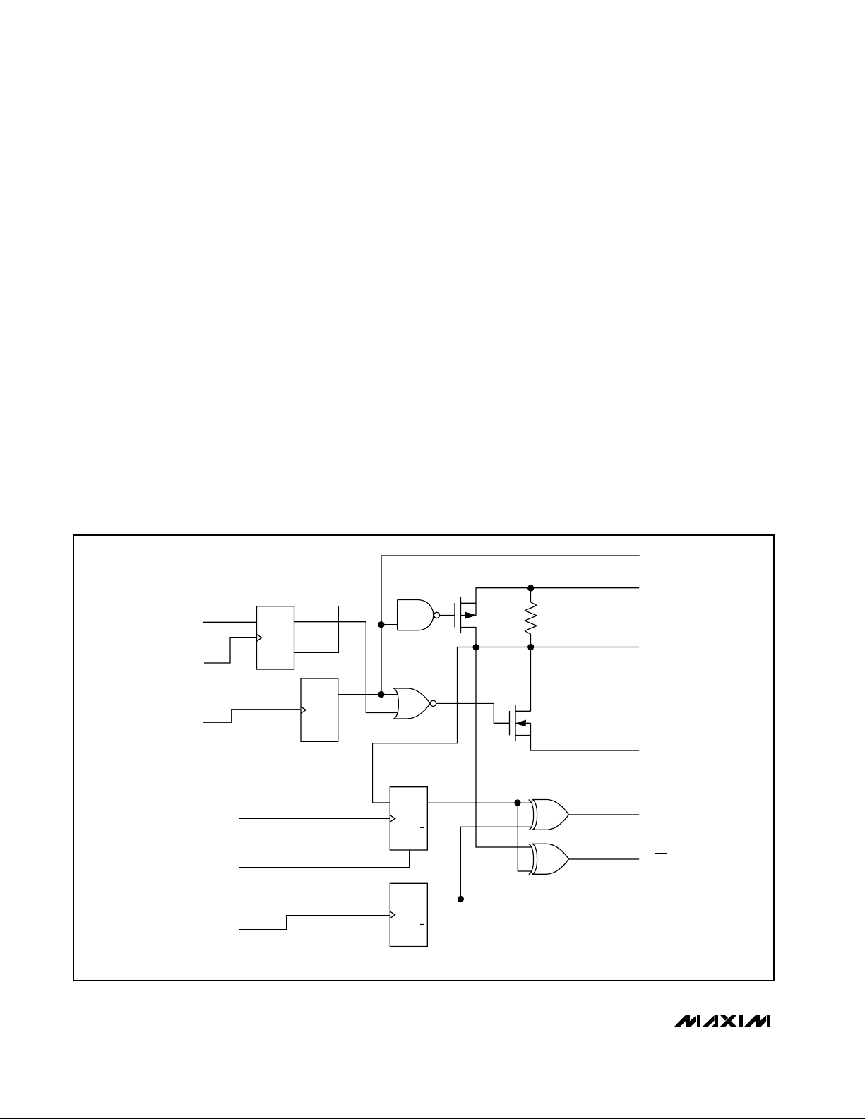
Input/Output Port
When an I/O is configured as an input, FETs Q1 and Q2
are off (Figure 10), creating a high-impedance input with
a nominal 100kΩ pullup to V+. All inputs are overvoltage
protected to 5.5V, independent of supply voltage. When
a port is configured as an output, either Q1 or Q2 is on,
depending on the state of the output port register. When
V+powers up, an internal power-on reset sets all registers to their respective defaults (Table 1).
Input Port Registers
The input port registers (Table 2) are read-only ports.
They reflect the incoming logic levels of the pins,
regardless of whether the pin is defined as an input or
an output by the respective configuration register. A
read of the input port 1 register latches the current
value of I/O0–I/O7. A read of the input port 2 register
latches the current value of I/O8–I/O15. Writes to the
input port registers are ignored.
2-Wire-Interfaced 16-Bit I/O Port Expander
with Interrupt
10 ______________________________________________________________________________________
Figure 10. Simplified Schematic of I/Os
CONFIGURATION
REGISTER
DATA FROM
SHIFT REGISTER
WRITE
CONFIGURATION
PULSE
DATA FROM
SHIFT REGISTER
WRITE PULSE
READ PULSE
POWER-ON
RESET
DATA FROM
SHIFT REGISTER
WRITE POLARITY
PULSE
D
SET
CLR
Q
Q
SET
D
CLR
OUTPUT PORT
REGISTER
Q
Q
INPUT PORT
REGISTER
SET
D
Q
Q
CLR
SET
D
Q
Q
CLR
POLARITY INVERSION
REGISTER
OUTPUT PORT
REGISTER DATA
V
DD
Q1
Q2
100kΩ
POLARITY
REGISTER
DATA
I/O PIN
V
SS
INPUT PORT
REGISTER DATA
TO INT
Page 11
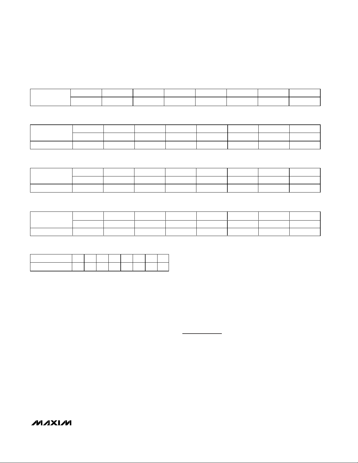
Output Port Registers
The output port registers (Table 3) set the outgoing
logic levels of the I/Os defined as outputs by the
respective configuration register. Reads from the output port registers reflect the value that is in the flip-flop
controlling the output selection, not the actual I/O value.
Polarity Inversion Registers
The polarity inversion registers (Table 4) enable polarity
inversion of pins defined as inputs by the respective
port configuration registers. Set the bit in the polarity
inversion register to invert the corresponding port pin’s
polarity. Clear the bit in the polarity inversion register to
retain the corresponding port pin’s original polarity.
Configuration Registers
The configuration registers (Table 5) configure the
directions of the I/O pins. Set the bit in the respective
configuration register to enable the corresponding port
as an input. Clear the bit in the configuration register to
enable the corresponding port as an output.
Bus Timeout
Set register 0x08 LSB (bit 0) to enable the bus timeout
function (Table 6) or clear it to disable the bus timeout
function. Enabling the timeout feature resets the
MAX7311 serial bus interface when SCL stops either high
or low during a read or write. If either SCL or SDA is low
for more than 29ms after the start of a valid serial transfer,
the interface resets itself and sets up SDA as an input.
The MAX7311 then waits for another START condition.
Standby
The MAX7311 goes into standby when the I2C bus is
idle. Standby supply current is typically 2.9µA.
Applications Information
Power-Supply Consideration
The MAX7311 operates from a supply voltage of 2V to
5.5V. Bypass the power supply to GND with a 0.047µF
capacitor as close to the device as possible.
MAX7311
2-Wire-Interfaced 16-Bit I/O Port Expander
with Interrupt
______________________________________________________________________________________ 11
Table 2. Registers 0x00, 0x01—Input Port Registers
Table 3. Registers 0x02, 0x03—Output Port Registers
Table 4. Registers 0x04, 0x05—Polarity Inversion Registers
Table 5. Registers 0x06, 0x07—Configuration Registers
Table 6. Register 0x08—Timeout Register
BIT
BIT
Power-up default 1 1111111
BIT
Power-up default 0 0000000
BIT
Power-up default 1 1 1 1 1 1 1 1
I7 I6 I5 I4 I3 I2 I1 I0
I15 I14 I13 I12 I11 I10 I9 I8
O7 O6 O5 O4 O3 O2 O1 O0
O15 O14 O13 O12 O11 O10 O9 O8
I/O7 I/O6 I/O5 I/O4 I/O3 I/O2 I/O1 I/O0
I/O15 I/O14 I/O13 I/O12 I/O11 I/O10 I/O9 I/O8
I/O7 I/O6 I/O5 I/O4 I/O3 I/O2 I/O1 I/O0
I/O15 I/O14 I/O13 I/O12 I/O11 I/O10 I/O9 I/O8
BIT 76543210
Power-up default 00000001
Page 12
MAX7311
2-Wire-Interfaced 16-Bit I/O Port Expander
with Interrupt
12 ______________________________________________________________________________________
Table 7. MAX7311 Address Map
AD2 AD1 AD0 A6 A5 A4 A3 A2 A1 A0 ADDRESS (HEX)
GNDSCLGND0010000 0x20
GND SCL V
GNDSDAGND0010010 0x24
GND SDA V
+
V
+
V
+
V
+
V
SCLGND0010100 0x28
SCL V
SDAGND0010110 0x2C
SDA V
GNDSCLSCL0011000 0x30
GNDSCLSDA0011001 0x32
GNDSDASCL0011010 0x34
GNDSDASDA0011011 0x36
+
V
+
V
+
V
+
V
SCLSCL0011100 0x38
SCLSDA0011101 0x3A
SDASCL0011110 0x3C
SDASDA0011111 0x3E
GNDGNDGND0100000 0x40
GND GND V
GND V
GND V
+
V
+
V
+
V
+
V
+
+
GNDGND0100100 0x48
GND V
+
V
+
V
GNDGNDSCL0101000 0x50
GNDGNDSDA0101001 0x52
GND V
GND V
+
V
+
V
+
V
+
V
+
+
GNDSCL0101100 0x58
GNDSDA0101101 0x5A
+
V
+
V
+
+
+
+
+
0010001 0x22
0010011 0x26
0010101 0x2A
0010111 0x2E
0100001 0x42
GND0100010 0x44
+
V
+
0100011 0x46
0100101 0x4A
GND0100110 0x4C
+
V
0100111 0x4E
SCL0101010 0x54
SDA0101011 0x56
SCL0101110 0x5C
SDA0101111 0x5E
Page 13
MAX7311
2-Wire-Interfaced 16-Bit I/O Port Expander
with Interrupt
______________________________________________________________________________________ 13
Table 7. MAX7311 Address Map (continued)
Chip Information
TRANSISTOR COUNT: 12,994
PROCESS: BiCMOS
AD2 AD1 AD0 A6 A5 A4 A3 A2 A1 A0 ADDRESS (HEX)
SCLSCLGND1010000 0xA0
SCL SCL V
+
1010001 0xA2
SCLSDAGND1010010 0xA4
SCL SDA V
+
1010011 0xA6
SDASCLGND1010100 0xA8
SDA SCL V
+
1010101 0xAA
SDASDAGND1010110 0xAC
SDA SDA V
+
1010111 0xAE
SCLSCLSCL1011000 0xB0
SCLSCLSDA1011001 0xB2
SCLSDASCL1011010 0xB4
SCLSDASDA1011011 0xB6
SDASCLSCL1011100 0xB8
SDASCLSDA1011101 0xBA
SDASDASCL1011110 0xBC
SDASDASDA1011111 0xBE
SCLGNDGND1100000 0xC0
SCL GND V
SCL V
SCL V
+
+
+
1100001 0xC2
GND1100010 0xC4
+
V
1100011 0xC6
SDAGNDGND1100100 0xC8
SDA GND V
SDA V
SDA V
+
+
+
1100101 0xCA
GND1100110 0xCC
+
V
1100111 0xCE
SCLGNDSCL1101000 0xD0
SCLGNDSDA1101001 0xD2
SCL V
SCL V
+
+
SCL1101010 0xD4
SDA1101011 0xD6
SDAGNDSCL1101100 0xD8
SDAGNDSDA1101101 0xDA
SDA V
SDA V
+
+
SCL1101110 0xDC
SDA1101111 0xDE
Page 14

MAX7311
2-Wire-Interfaced 16-Bit I/O Port Expander
with Interrupt
14 ______________________________________________________________________________________
Package Information
(The package drawing(s) in this data sheet may not reflect the most current specifications. For the latest package outline information,
go to www.maxim-ic.com/packages
.)
N
1
TOP VIEW
e
FRONT VIEW
INCHES
MIN
DIM
0.093A
0.004
A1
0.014
B
0.009
C
H
E
D
A
B
A1
C
L
e 0.050 1.27
0.291
E
H 0.4190.394 10.00 10.65
0.016L
VARIATIONS:
INCHES
MINDIM
D
0.398 0.413 AA10.5010.10 16
D
0.447 0.463 AB11.7511.35 18
D 0.6140.598 15.20 2415.60 AD
D 0.7130.697 17.70 2818.10 AE
0∞-8∞
MAX
0.104
0.012
0.019
0.013
0.299
0.050
MAX
0.5120.496D
MILLIMETERS
MAX
MIN
2.65
2.35
0.30
0.10
0.49
0.35
0.23
0.32
7.40 7.60
0.40 1.27
MILLIMETERS
MAX
MIN
12.60 13.00
N MS013
20
AC
SOICW.EPS
SIDE VIEW
PROPRIETARY INFORMATION
TITLE:
PACKAGE OUTLINE, .300" SOIC
REV.DOCUMENT CONTROL NO.APPROVAL
21-0042
1
B
1
Page 15

MAX7311
2-Wire-Interfaced 16-Bit I/O Port Expander
with Interrupt
______________________________________________________________________________________ 15
Package Information (continued)
(The package drawing(s) in this data sheet may not reflect the most current specifications. For the latest package outline information,
go to www.maxim-ic.com/packages
.)
e
D
12
MAX
0.078
0.008
0.015
0.008
0.212
0.311
0.037
8∞
MILLIMETERS
MAX
MIN
1.73 1.99
0.21
0.05
0.38
0.25
0.20
0.09
5.38
5.20
0.65 BSC
7.65
7.90
0.63
0.95
0∞
8∞
MAX
0.249
0.249
0.289
0.328
0.407
MILLIMETERS
MAX
MIN
6.07
6.33
6.07
6.33
7.07
7.33
8.07
8.33
10.07
10.33
N
14L
16L
20L
24L
28L
C
INCHES
MIN
D
0.239
D
0.239
D
0.278
D
0.317
0.397
D
INCHES
DIM
MIN
A
0.068
A1
0.002
B
0.010
C
HE
N
A
B
A1
D
E
e
H
L
0.004
SEE VARIATIONS
0.205
0.0256 BSC
0.301
0.025
0∞
L
SSOP.EPS
NOTES:
1. D&E DO NOT INCLUDE MOLD FLASH.
2. MOLD FLASH OR PROTRUSIONS NOT TO EXCEED .15 MM (.006").
3. CONTROLLING DIMENSION: MILLIMETERS.
4. MEETS JEDEC MO150.
5. LEADS TO BE COPLANAR WITHIN 0.10 MM.
PROPRIETARY INFORMATION
TITLE:
PACKAGE OUTLINE, SSOP, 5.3 MM
21-0056
REV.DOCUMENT CONTROL NO.APPROVAL
1
C
1
Page 16

MAX7311
2-Wire-Interfaced 16-Bit I/O Port Expander
with Interrupt
16 ______________________________________________________________________________________
Package Information (continued)
(The package drawing(s) in this data sheet may not reflect the most current specifications. For the latest package outline information,
go to www.maxim-ic.com/packages
.)
TSSOP4.40mm.EPS
Page 17

MAX7311
2-Wire-Interfaced 16-Bit I/O Port Expander
with Interrupt
Maxim cannot assume responsibility for use of any circuitry other than circuitry entirely embodied in a Maxim product. No circuit patent licenses are
implied. Maxim reserves the right to change the circuitry and specifications without notice at any time.
Maxim Integrated Products, 120 San Gabriel Drive, Sunnyvale, CA 94086 408-737-7600 ____________________ 17
© 2003 Maxim Integrated Products Printed USA is a registered trademark of Maxim Integrated Products.
Package Information (continued)
(The package drawing(s) in this data sheet may not reflect the most current specifications. For the latest package outline information,
go to www.maxim-ic.com/packages
.)
24L QFN THIN.EPS
PACKAGE OUTLINE
12,16,20,24L QFN THIN, 4x4x0.8 mm
21-0139 A
PACKAGE OUTLINE
12,16,20,24L QFN THIN, 4x4x0.8 mm
A21-0139
 Loading...