

Page 1
19-0107; Rev 3; 9/95
Switch-Mode DC-DC Regulators
_______________General Description
The MAX724/MAX726 are monolithic, bipolar, pulsewidth modulation (PWM), switch-mode DC-DC regulators optimized for step-down applications. The
MAX724 is rated at 5A, and the MAX726 at 2A. Few
external components are needed for standard operation because the power switch, oscillator, and control
circuitry are all on-chip. Employing a classic buck
topology, these regulators perform high-current stepdown functions, but can also be configured as inverters, negative boost converters, or flyback converters.
These regulators have excellent dynamic and transient
response characteristics, while featuring cycle-by-cycle
current limiting to protect against overcurrent faults and
short-circuit output faults. The MAX724/MAX726 also
have a wide 8V to 40V input range in the buck stepdown configuration. In inverting and boost configurations, the input can be as low as 5V.
The MAX724/MAX726 are available in a 5-pin TO-220
package. The devices have a preset 100kHz oscillator
frequency and a preset current limit of 6.5A (MAX724)
or 2.6A (MAX726).
_______________________Applications
Distributed Power from High-Voltage Buses
High-Current, High-Voltage Step-Down Applications
High-Current Inverter
Negative Boost Converter
Multiple-Output Buck Converter
Isolated DC-DC Conversion
5A/2A Step-Down, PWM,
___________________________Features
♦ Input Range: Up to 40V
♦ 5A On-Chip Power Switch (MAX724)
2A On-Chip Power Switch (MAX726)
♦ Adjustable Output: 2.5V to 35V
♦ 100kHz Switching Frequency
♦ Excellent Dynamic Characteristics
♦ Few External Components
♦ 8.5mA Quiescent Current
♦ TO-220 Package
______________Ordering Information
PART TEMP. RANGE PIN-PACKAGE
MAX724CCK
MAX724ECK -40°C to+85°C 5 TO-220
MAX726CCK
MAX726ECK -40°C to+85°C 5 TO-220
0°C to+70°C 5 TO-220
0°C to+70°C 5 TO-220
MAX724/MAX726
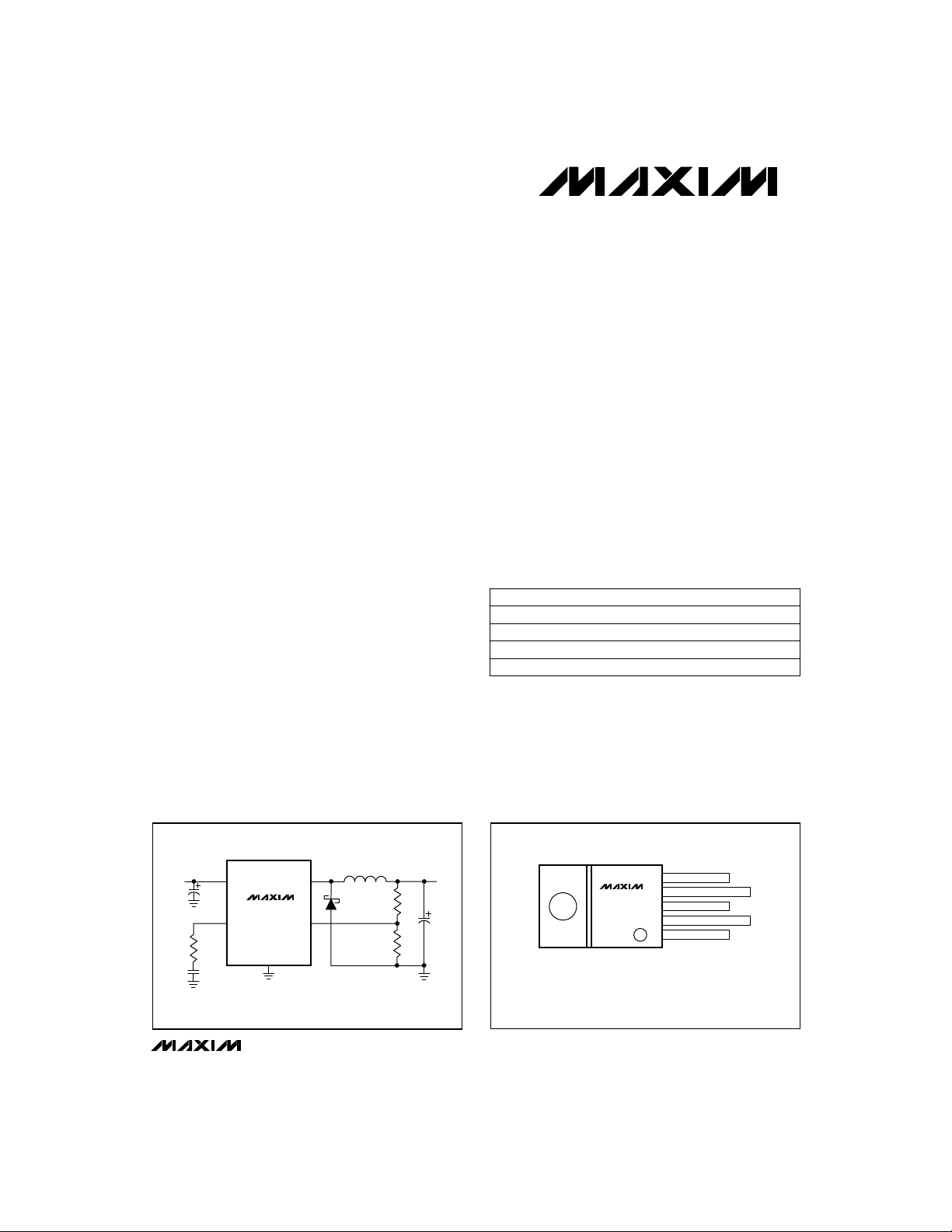
__________Typical Operating Circuit
INPUT
8V TO 40V
220µF
2.7k
V
IN
V
C
0.01µF
5A STEP-DOWN CONVERTER
V
SW
MAX724
FB
GND
________________________________________________________________
50µH
MBR745
2.21k
2.8k
OUTPUT
5V AT 5A
470µF
__________________Pin Configuration
FRONT VIEW
MAX724
MAX726
5-PIN TO-220
CASE IS CONNECTED TO GROUND.
STANDARD PACKAGE HAS STAGGERED LEADS.
CONTACT FACTORY FOR STRAIGHT LEADS.
Maxim Integrated Products
Call toll free 1-800-998-8800 for free samples or literature.
V
GND
FB
IN
V
SW
V
C
1
5
4
3
2
1
Page 2
5A/2A Step-Down, PWM,
Switch-Mode DC-DC Regulators
ABSOLUTE MAXIMUM RATINGS
Input Voltage..................................................45V
Switch Voltage with Respect to Input Voltage................50V
Switch Voltage with Respect to Ground Pin (V
(Note 1) .....................................................35V
Feedback Pin Voltage................................-0.3V, +10V
Operating Temperature Ranges
MAX72_CCK .....................................0°C to +70°C
MAX72_ECK....................................-40°C to +85°C
Stresses beyond those listed under “Absolute Maximum Ratings” may cause permanent damage to the device. These are stress ratings only, and functional
operation of the device at these or any other conditions beyond those indicated in the operational sections of the specifications is not implied. Exposure to
absolute maximum rating conditions for extended periods may affect device reliability.
Negative)
SW
ELECTRICAL CHARACTERISTICS
(VIN= 25V, Tj= T
MAX724/MAX726
Input Supply Voltage Range 8.0 40.0 V
Switch-On Voltage (Note 2)
Switch-Off Leakage
Minimum Supply Voltage
Switch-Current Limit (Note 5) A
Switching Frequency kHz
to T
MIN
PARAMETER CONDITIONS MIN TYP MAX UNITS
, unless otherwise noted.)
MAX
MAX724
MAX726
MAX724
MAX726
VFB= 2.5V, VIN≤ 40V 8.5 11Supply Current (Note 3) mA
Normal Mode 7.3 8.0
Start-Up Mode (Note 4)
MAX724 5.5 6.5 8.5
MAX726 2.0 2.6 3.2
VFB= grounded through 2kΩ (Note 5)
8V ≤ VIN≤ 40V
ISW= 1A
ISW= 5A
ISW= 0.5A
ISW= 2A
VIN≤ 25V, VSW= 0V
VIN= 40V, VSW= 0V
VIN≤ 25V, VSW= 0V
VIN= 40V, VSW= 0V
Junction Temperature Ranges
MAX72_CCK ....................................0°C to +125°C
MAX72_ECK..................................-40°C to +125°C
Storage Temperature Range ...................-65°C to +160°C
Lead Temperature (soldering, 10sec)....................+300°C
Tj≥ 0°C
Tj< 0°C
Tj≥ 0°C
Tj< 0°C
Tj= +25°C
Tj= +25°C
Tj= +25°C
Tj= +25°C
Tj≥ 0°C
Tj< 0°C
Tj= +25°C
Tj≤ +125°C
Tj= +25°C
85 90Maximum Duty Cycle %
90 100 110
85 120
1.85
2.10
2.30
2.50
1.2
1.7
5 300
10 500
150
250
3.5 4.8
3.5 5.0
20
0.03 0.1Switching Frequency Line Regulation %/V
V
µA
V
V
2 _______________________________________________________________________________________
Page 3
5A/2A Step-Down, PWM,
Switch-Mode DC-DC Regulators
ELECTRICAL CHARACTERISTICS (continued)
(VIN= 25V, Tj= T
Error-Amplifier Voltage Gain
Error-Amplifier Transconductance
Error-Amplifier Source Current
Error-Amplifier Sink Current
Feedback Pin Bias Current
Reference Voltage
Reference Voltage Tolerance
Reference Voltage Line Regulation
VC Voltage at 0% Duty Cycle
Thermal Resistance,
Junction to Case (Note 6)
Note 1: Do not exceed switch-to-input voltage limitation.
Note 2: For switch currents between 1A and 5A (2A for MAX726), maximum switch-on voltage can be calculated via linear
interpolation.
Note 3: By setting the feedback pin (FB) to 2.5V, the V
zero, approximating the zero load condition.
Note 4: For proper regulation, total voltage from V
Note 5: To avoid extremely short switch-on times, the switch frequency is internally scaled down when V
current limit is tested with V
Note 6: Guaranteed, not production tested.
to T
MIN
, unless otherwise noted.)
MAX
PARAMETER CONDITIONS MIN TYP MAX UNITS
1V ≤ VC≤ 4V Tj= +25°C
Tj= +25°C
VFB= 2V
VFB= 2.5V
Tj= +25°C
Tj= +25°C
VFB= VREF
VC= 2V
VREF (nominal) = 2.21V
Tj= +25°C
All conditions of input voltage, output voltage,
temperature and load current
8V ≤ VIN≤ 40V
Tj= +25°C
Tj= T
MIN
to T
MAX
2000 V/V
3000 5000 9000 µmho
100 140 225 µA
0.6 1.0 1.7 mA
0.5 2 µA
2.155 2.210 2.265 V
±0.5 ±1.5
±1.0 ±2.5
0.005 0.02 %/V
1.5 V
-4 mV/°C
MAX724 2.5
MAX726 4.0
pin is forced to its low clamp level and the switch duty cycle is forced to
C
to GND must be ≥ 8V after start-up.
IN
adjusted to give a 1µs minimum switch-on time.
FB
is less than 1.3V. Switch-
FB
MAX724/MAX726
%
°C/W
__________________________________________Typical Operating Characteristics
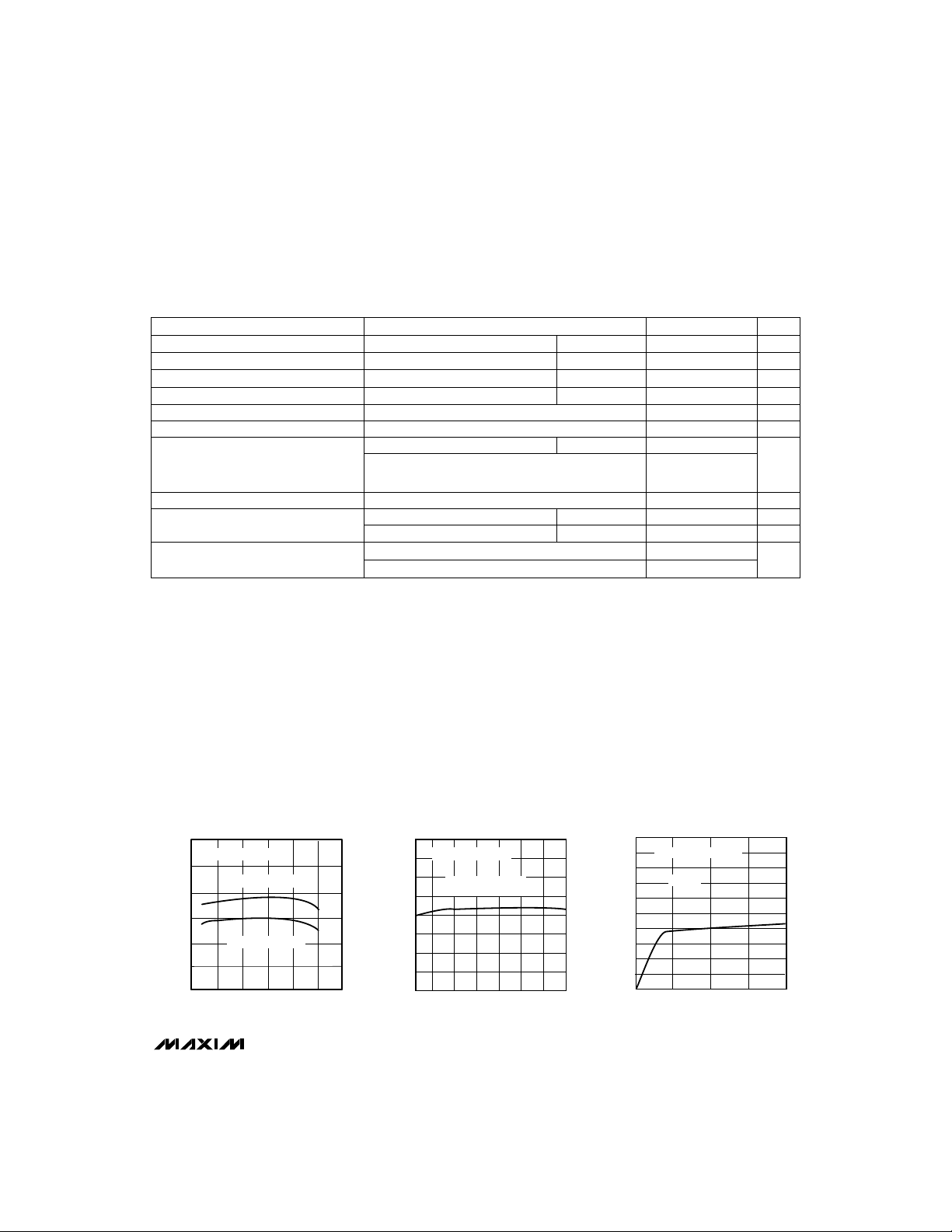
STEP-DOWN CONVERTER EFFICIENCY
110
100
90
80
EFFICIENCY (%)
70
60
50
06
MAX724
vs. OUTPUT CURRENT
CIRCUIT OF FIGURE 2
V
= 12V, VIN = 20V
OUT
V
= 5V, VIN = 15V
OUT
135
2
OUTPUT CURRENT (A)
4
16
14
12
10
8
6
SUPPLY CURRENT (mA)
4
2
0
-40 100
_______________________________________________________________________________________ 3
SUPPLY CURRENT
vs. JUNCTION TEMPERATURE
CIRCUIT OF FIGURE 2
VIN = 25V, V
I
OUT
-25 25 75
0
JUNCTION TEMPERATURE (°C)
= 1mA
= 5V
OUT
50
QUIESCENT SUPPLY CURRENT (mA)
125
QUIESCENT SUPPLY CURRENT
20
18
16
14
12
10
8
6
4
2
0
vs. INPUT VOLTAGE
DEVICE NOT SWITCHING
VC = 1V
0
10 30
V
IN
20
INPUT VOLTAGE (V)
40
Page 4
5A/2A Step-Down, PWM,
Switch-Mode DC-DC Regulators
____________________________Typical Operating Characteristics (continued)
REFERENCE VOLTAGE
vs. JUNCTION TEMPERATURE
2.25
2.24
2.23
2.22
2.21
2.20
2.19
REFERENCE VOLTAGE (V)
2.18
MAX724/MAX726
2.17
-25 25 75
-40 100
JUNCTION TEMPERATURE (°C)
8000
7000
6000
5000
4000
3000
2000
TRANSCONDUCTANCE (µmho)
1000
0
50
0
ERROR-AMPLIFIER PHASE AND g
PHASE
1k
g
M
10k 1M
100k
FREQUENCY (Hz)
125
SWITCHING FREQUENCY
vs. JUNCTION TEMPERATURE
120
115
110
105
100
95
90
SWITCHING FREQUENCY (kHz)
85
80
-25 25 75
0
-40 100
JUNCTION TEMPERATURE (°C)
M
200
150
100
50
0
-50
PHASE (degrees)
-100
-150
-200
10M
50
SWITCHING FREQUENCY (kHz)
SWITCH-ON VOLTAGE (V)
125
SWITCHING FREQUENCY
vs. FEEDBACK PIN VOLTAGE
160
140
120
100
-40°C
80
60
40
20
0
0
0.5 1.5
SWITCH-ON VOLTAGE
3.0
2.5
2.0
1.5
1.0
0.5
1.0
vs. SWITCH CURRENT
Tj = +25°C
MAX724
MAX726
06
135
2
SWITCH CURRENT (A)
+125°C
+25°C
FB VOLTAGE (V)
2.0
4
2.5 3.0
FB CURRENT (µA)
500
400
300
200
100
0
-100
-200
-300
-400
-500
FEEDBACK PIN CURRENT
vs. FB VOLTAGE
START OF FREQUENCY
SHIFTING
0
13
2
FB VOLTAGE (V)
4
56
OUTPUT CURRENT LIMIT (A)
78910
OUTPUT CURRENT LIMIT
8
7
5
4
3
2
1
0
-40
-25 2560
JUNCTION TEMPERATURE (°C)
vs. TEMPERATURE
MAX724
MAX726
50
75
4 _______________________________________________________________________________________
100 125
Page 5

5A/2A Step-Down, PWM,
Switch-Mode DC-DC Regulators
______________________________________________________________Pin Description
MAX724/MAX726
PIN
Feedback Input is the error amplifier's inverting input, and controls output voltage by adjusting switch duty cycle.
FB1
Input bias current is typically 0.5µA when the error amplifier is balanced (I
by reducing the oscillator frequency when the output voltage is low. (See the
Error-Amplifier Output. A series RC network connected to this pin compensates the MAX724/MAX726. Output
V
2
4
5
swing is limited to about 5.8V in the positive direction and -0.7V in the negative direction. V
C
nize the MAX724/MAX726 to an external clock. (See the
Ground requires a short low-noise connection to ensure good load regulation. The internal reference is referred
GND3
to GND, so errors at this pin are multiplied by the error amplifier. See the
grounding details.
Internal Power Switch Output. The Switch output can swing 35V below ground and is rated for 5A (MAX724), 2A
V
SW
(MAX726).
VINsupplies power to the MAX724/MAX726's internal circuitry and also connects to the collector. VINmust be
V
IN
bypassed with a low-ESR capacitor, typically 200µF or 220µF.
_________________Detailed Description
The MAX724/MAX726 are complete, single-chip, pulsewidth modulation (PWM), step-down DC-DC converters
(Figure 1). All oscillator (100kHz), control, and currentlimit circuitry, including a 5A power switch (2A for
MAX726), are included on-chip. The oscillator turns on
the switch (VSW) at the beginning of each clock cycle.
The switch turns off at a point later in the clock cycle,
which is a function of the signal provided by the error
amplifier. The maximum switch duty cycle is approximately 93% at the MAX724/MAX726's 100kHz switching frequency.
Both the input (FB) and output (V
amplifier are brought out to simplify compensation.
Most applications require only a single series RC
network connected from VCto ground. The error
amplifier is a transconductance amplifier with a gMof
approximately 5000µmho. When slewing, VCcan
source about 140µA, and sink about 1.1mA. This
asymmetry helps minimize start-up overshoot by
allowing the amplifier output to slew more quickly in
the negative direction.
Current limiting is provided by the current-limit comparator. If the current-limit threshold is exceeded, the
switch cycle terminates within about 600ns. The current-limit threshold is internally set to approximately
) of the error
C
FUNCTIONNAME
= 0V). FB also aids current limiting
OUT
Applications Information
can also synchro-
Applications Information
Applications Information
6.5A (2.6A for MAX726). V
driven by the PWM controller circuitry. VSWcan swing
C
section).
is a power NPN, internally
SW
section.)
section for
35V below ground and is rated for 5A (2A for MAX726).
Basic Step-Down Application
Figure 2 shows the MAX724/MAX726 in a basic stepdown DC-DC converter. Typical MAX724 waveforms
are shown in Figure 3 for VIN= 20V, V
50µH, and I
forms are shown. One set shows high load current (3A)
= 3A and 0.16A. Two sets of wave-
OUT
OUT
= 5V, L =
where inductor current never falls to zero during the
switch "off-cycle" (continuous-conduction mode, CCM).
The second set of waveforms, at low output current
(0.16A), shows inductor current at zero during the latter
half of the switch off-cycle (discontinuous-conduction
mode, DCM). The transition from CCM to DCM occurs
at an output current (I
following equation:
(V
I
DCM
where V
voltage drop across the switch, and f
OUT
=
is the diode forward voltage drop, VSWis the
D
most applications, the distinction between CCM and
) that can be derived with the
DCM
+ VD) [(VIN- VSW) - (V
2 (V
- VSW) f
IN
OSC
L
OSC
OUT+VD
)]
= 100kHz. In
DCM is academic since actual performance differences
are minimal. All CCM designs can be expected to exhibit
DCM behavior at some level of reduced load current.
_______________________________________________________________________________________ 5
Page 6

5A/2A Step-Down, PWM,
Switch-Mode DC-DC Regulators
In DCM, ringing occurs at VSWin the latter part of the
switch off-cycle. This is due to the inductor resonating
with the parallel capacitance of the catch diode and the
VSWnode. This ringing is harmless and does not
appear at the output. Furthermore, attempts to damp
this ringing by adding circuitry will reduce efficiency
and are not advised. No off-state ringing occurs in
CCM because the diode always conducts during the
switch-off time and consequently damps any resonance at VSW.
MAX724/MAX726
FB
V
C
2.21V
REF
ERROR
AMPLIFIER
INTERNAL
BIAS
MAX724
Figure 1. MAX724 Block Diagram
INPUT
8V TO 40V
220µF
V
IN
MAX724
MAX726
V
C
R3
0.01µF
2.7k
C2
GND
Figure 2. Basic Step-Down Converter
100kHz
OSCILLATOR
GND
V
SW
FB
CURRENT-LIMIT
PWM
LOGIC
CONTROL
L
50µH (MAX724)
100µH (MAX726)
D
MBR745
COMPARATOR
SWITCH
5V at 5A (MAX724)
5V at 2A (MAX726)
R1
2.8k
R2
2.2k
OUTPUT
V
V
SW
C1
470µF
IN
_______________Component Selection
Table 1 lists component suppliers for inductors, capacitors, and diodes appropriate for use with the
MAX724/MAX726. Be sure to observe specified ratings
for all components.
Table 1. Component Suppliers
Surface-Mount Components (for designs typically below 2A)
Inductors: Sumida Electric - CDR125 Series
Capacitors: Matsuo - 267 series
Diodes: Motorola - MBRS series
Through-Hole Components
Inductors: Sumida - RCH-110 series
Capacitors: Nichicon - PL series low-ESR electrolytics
Diodes: General Purpose - 1N5820-1N5825
USA: Phone (708) 956-0666
Japan: Phone 81-3607-5111
Coiltronics - CTX series
Sprague - 595D series
Nihon - NSQ series
Cadell-Burns - 7070, 7300, 6860, and 7200 series
Renco - various series
Coiltronics - various series
United Chemi-Con - LXF series
Sanyo - OS-CON low-ESR organic semiconductor
Motorola - MBR and MBRD series
FAX 81-3607-5144
USA: Phone (305) 781-8900
FAX (305) 782-4163
USA: Phone (714) 969-2491
FAX (714) 960-6492
Japan: Phone 81-6337-6450
USA: Phone (603) 224-1961
FAX (603) 224-1430
USA: Phone (602) 244-5303
FAX (602) 244-4015
USA: Phone (805) 867-2555
FAX (805) 867-2556
Japan: Phone 81-3-3494-7411
FAX 81-3-3494-7414
(see above for phone number)
USA: Phone (516) 746-2310
FAX (516) 742-2416
USA: Phone (516) 586-5566
FAX (516) 586-5562
(see above for phone number)
USA: Phone (708) 843-7500
FAX (708) 843-2798
Japan: Phone 81-7-5231-8461
FAX 81-7-5256-4158
USA: Phone (714) 255-9500
FAX (714) 255-9400
USA: Phone (619) 661-6835
FAX (619) 661-1055
Japan: Phone 81-7-2070-6306
FAX 81-7-2070-1174
(see above for phone number)
6 _______________________________________________________________________________________
Page 7

Switch-Mode DC-DC Regulators
Inductor Selection
Although most MAX724 designs perform satisfactorily
with 50µH inductors (100µH for the MAX726), the
MAX724/MAX726 are able to operate with values ranging from 5µH to 200µH. In some cases, inductors other
than 50µH may be desired to minimize size (lower
inductance), or reduce ripple (higher inductance). In
any case, inductor current must at least be rated for the
desired output current.
In high-current applications, pay particular attention to
both the RMS and peak inductor ratings. The inductor's peak current is limited by core saturation.
Exceeding the saturation limit actually reduces the
coil's inductance and energy storage ability, and
increases power loss. Inductor RMS current ratings
depend on heating effects in the coil windings.
The following equation calculates maximum output current as a function of inductance and input conditions:
V
I
= ISW-
OUT
where I
MAX724), VINis the maximum input voltage, V
is the maximum switch current (5.5A for
SW
output voltage, and f
OUT(VIN
is the switching frequency.
OSC
For the MAX724 example in Figure 2, with L = 50µH
= 25V,
and V
IN
I
OUT
= 5.5A -
5V (25V - 5V)
2 (105Hz) 25V (50 x 10-6H)
Note that increasing or decreasing inductor value provides only small changes in maximum output current
(100µH = 5.3A, 20µH = 4.5A). The equation shows that
output current is mostly a function of the
MAX724/MAX726 current-limit value. Again, a 50µH
inductor works well in most applications and provides
5A with a wide range of input voltages.
D1 provides a path for inductor current when VSWturns
off. Under normal load conditions, the average diode
current may only be a fraction of load current; but during short-circuit or current-limit, diode current is higher.
Conservative design dictates that the diode average
current rating be 2 times the desired output current. If
operation with extended short-circuit or overload time is
expected, then the diode current rating must exceed
the current limit (6.5A = MAX724, 2.6A = MAX726), and
heat sinking may be necessary.
Under normal operating conditions (not shorted), power
dissipated in the diode P
is calculated by:
D
2 f
OSCVIN
- V
)
OUT
L
Catch Diode
OUT
is the
= 5.1A
5A/2A Step-Down, PWM,
PD= I
(VIN- V
OUT
where VDis forward drop of the diode at a current
equal to I
provide the best performance and are recommended
. In nearly all circuits, Schottky diodes
OUT
due to their fast switching times and low forward voltage
drop. Standard power rectifiers such as the 1N4000
series are too slow for DC-DC conversion circuits and are
not recommended.
Output Filter Capacitor
For most MAX724/MAX726 applications, a high-quality,
low-ESR, 470µF or 500µF output filter capacitor will suffice. To reduce ripple, minimize capacitor lead length
and connect the capacitor directly to the GND pin.
Capacitor suppliers are listed in Table 1. Output ripple
is a function of inductor value and output capacitor
effective series resistance (ESR). In continuous-conduction mode:
ESR (V
V
CR(p-p)
=
OUT
It is interesting to note that input voltage (VIN), and not
load current, affects output ripple in CCM. This is
because only the DC, and not the peak-to-peak, inductor current changes with load (see Figure 3).
In discontinuous-conduction mode, the equation is different because the peak-to-peak inductor current does
depend on load:
= ESR
√
V
DR(p-p)
2 I
OUTVOUT(VIN
where output ripple is proportional to the square root of
load current. Refer to the earlier equation for I
determine where DCM occurs and hence when the
DCM ripple equation should be used.
Input Bypass Capacitor
An input capacitor (200µF or 220µF) is required for stepdown converters because the input current, rather than
being continuous (like output current), is a square wave.
For this reason the capacitor must have low ESR and a
ripple-current rating sufficiently large so that its ESR and
the AC input current do not conspire to overheat the
capacitor. In CCM, the capacitor's RMS ripple current is:
= I
OUT
√
I
R(RMS)
V
The power dissipated in the input capacitor is then PC:
PC= I
R(RMS)
OUT
V
IN
) (1 - V
L f
OSC
L f
OUT(VIN
V
2
(ESR)
) V
D
OUT/VIN
OSCVIN
- V
OUT
2
IN
- V
)
OUT
)
)
to
DCM
MAX724/MAX726
_______________________________________________________________________________________ 7
Page 8

5A/2A Step-Down, PWM,
Switch-Mode DC-DC Regulators
CONTINUOUS-CURRENT MODE (I
V
D
0
-0.5
IP = 3.4A
MAX724/MAX726
I
SW
0
IP = 3.4A
I
= I
= 3A
AVG
OUT
0
IP = 3.4A
OUT
= 3A)
I
L
VSW VOLTAGE (TO GND)
(ALSO DIODE VOLTAGE)
5V/div
SWITCH CURRENT
1A/div
INDUCTOR CURRENT
1A/div
DISCONTINUOUS-CURRENT MODE
(I
= 0.16A)
OUT
IP = 0.5A
I
D
0
I
= 2.1A
AVG
DIODE CURRENT
1A/div
Figure 3. MAX724 Step-Down Converter Waveforms with VIN= 20V, L = 50µH (all waveforms 2µs/div)
8 _______________________________________________________________________________________
Page 9

Switch-Mode DC-DC Regulators
Be sure that the selected capacitor can handle the ripple
current over the required temperature range. Also locate
the input capacitor very close to the MAX724/MAX726 and
use minimum length leads (surface-mount or radial
through-hole types). In most applications, ESR is more
important than actual capacitance value since electrolytic
capacitors are mostly resistive at the MAX724/MAX726's
100kHz switching frequency.
__________Applications Information
Setting Output Voltage
R1 and R2 set output voltage as follows:
V
R2
OUT
R1 =
2.21V is the reference voltage, so setting R2 to 2.21kΩ
(standard 1% resistor value) results in 1mA flowing
through R1 and R2 and simplifies the above equation.
Other values will also work for R2, but should not
exceed 4kΩ.
Synchronizing the Oscillator
The MAX724/MAX726 can be synchronized to an external 110kHz to 160kHz source by pulsing the VCpin to
ground at the desired clock rate. This is conveniently
done with the collector of an external grounded-emitter
NPN transistor. VCshould be pulled low for 300ns.
Doing this may have some impact on output regulation,
but the effect should be minimal for compensation
resistor values between 1kΩ and 4kΩ.
The MAX724/MAX726 draw about 7.5mA operating current, which is largely independent of input voltage or
load current. They draw an additional 5mA during
switch on-time. Power dissipated in the internal V
transistor is proportional to load current and depends
on both conduction losses (product of switch on-voltage and switch current) and dynamic switching losses
(due to switch rise and fall times). Total MAX724 power
dissipation can be calculated as follows:
P = VIN[7.5mA + 5mA (DC) + 2 I
. . . DC [I
(1.8V) + 0.1Ω (I
OUT
DC = Duty Cycle =
= Overlap Time = 50ns + (3ns/A) I
t
SW
where tSWis "overlap" time. Switch dissipation is
momentarily high during overlap time because both cur-
-R2
2.21V
Power Dissipation
OUTtSWfOSC
)2]
OUT
V
+ 0.5V
OUT
- 2V
V
IN
OUT
SW
] + . . .
5A/2A Step-Down, PWM,
rent and voltage appear across the switch at the same
time. t
the MAX724.
Power dissipation in the MAX726 can be estimated in
exactly the same way as the MAX724, except that 1.1V
(and not 1.8V) is a more reasonable value for the nominal voltage drop across the on-board power switch.
GND demands a short low-noise connection to ensure
good load regulation. Since the internal reference is
referred to GND, errors in the GND pin voltage get multiplied by the error amplifier and appear at the output.
If the MAX724/MAX726 GND pin is separated from the
negative side of the load, then high load return current
can generate significant error across a seemingly small
ground resistance. Single-point grounding is the most
effective way to eliminate these errors. A recommended ground arrangement is shown in Figure 4.
The VSWcurrent is internally limited to about 6.5A in the
MAX724 and 2.6A in the MAX726. In addition, another
feature of the MAX724/MAX726's overload protection
scheme is that the oscillator frequency is reduced
when the output voltage falls below approximately half
its regulated value. This is the case during short-circuit
and heavy overload conditions.
Since the minimum on-time for the switch is about
0.6µs, frequency reduction during overload ensures
that switch duty cycle can fall to a low enough value to
maintain control of output current. At the normal
100kHz switching frequency, an on-time as short as
HIGH CURRENT
RETURN PATH
Figure 4. Recommended Ground Connection
is approximately: [50ns + (3ns/A) (I
SW
Ground Connections
Overload Protection
MAX724
MAX726
FB
GND
R1
R2
)] for
OUT
NEGATIVE OUTPUT
NODE WHERE LOAD
REGULATION WILL
BE MEASURED
MAX724/MAX726
_______________________________________________________________________________________ 9
Page 10

5A/2A Step-Down, PWM,
Switch-Mode DC-DC Regulators
A series RC network connected from VCto ground
compensates the MAX724/MAX726. Compensation
RCvalues are shown in the applications circuits. R
and CCshape error-amplifier gain as follows: At DC,
RCand CChave no effect, so the error-amplifier's
gain is the product of its transconductance (approximately 5000µmhos) and an internal 400kΩ load
impedance (r
approximately 2000µmhos. RCand CCthen add a
INT
low-frequency pole and a high-frequency zero, as
shown in Figure 5.
GAIN
A
V(DC)
90° PHASE SHIFT
= gM(400kΩ) ≈ 2000
f
= 1/[2π(400kΩ)]C
POLE
-A
= gM / (2π f CC)
V(MID)
C
f
= 1 / (2π RC CC)
ZERO
Compensation Network
) at VC. So at DC, A
V(DC)
= gM(r
INT
C
) =
A
= gMR
V(HI)
C
MAX724/MAX726
Figure 5. Error-Amplifier Gain as Set by RCand CCat VCPin
FEEDBACK RESISTOR
MAIN FILTER CAP
Figure 6. Optional LC Output Filter
FREQUENCY
L
F
C
F
0.2µs would be needed to provide a narrow enough
duty cycle that could control current when the output is
shorted. Since 0.6µs is too long (at 100kHz), the f
is lowered to 20kHz once FB (and hence the output)
drops below about 1.3V (see Frequency vs. VFBVoltage
graph in the
Typical Operating Characteristics
way, the MAX724/MAX726's 0.6µs minimum tONallows
a sufficiently small duty cycle (at the reduced f
that current can still be limited.
TO LOAD
OSC
). This
) so
OSC
Output Overshoot
The MAX724/MAX726 error-amplifier design minimizes
overshoot, but precautions against overshoot should
still be exercised in sensitive applications. Worst-case
overshoot typically occurs when recovering from an
output short because VCslews down from its highest
voltage. This can be checked by simply shorting and
releasing the output.
Reduce objectional overshoot by increasing the compensation resistor (to 3kΩ or 4kΩ) at V
the error-amplifier output, VC, to move more rapidly in
. This allows
C
the negative direction. In some cases, loop stability
may suffer with a high-value compensation resistor. An
option, then, is to add output filter capacitance, which
reduces short-circuit recovery overshoot by limiting output rise time. Lowering the compensation capacitor to
below 0.05µF may also help by allowing VCto slew further before the output rises too far.
Optional Output Filters
Though not shown in the application circuits in Figures
2, 7, and 8, additional filtering can easily be added to
reduce output ripple to levels below 2%. It is more
effective to add an LC type filter rather than additional
output capacitance alone. A small-value inductor (2µH
to 10µH) and between 47µF and 220µF of filter capacitance should suffice (Figure 6). Although the inductor
does not need to be of high quality (it is not switching),
it must still be rated for the full load current.
When an LC filter is added, do not move the connection
of the feedback resistor to the LC output. It should be left
connected to the main output filter capacitor (C1 in Figure
2). If the feedback connection is moved to the LC filter
point, the added phase shift may impact stability.
10 ______________________________________________________________________________________
Page 11

Switch-Mode DC-DC Regulators
___________________Typical Applications
Positive-to-Negative DC-DC Inverter
The MAX724/MAX726 can convert positive input voltages to negative outputs if the sum of input and output
voltage is greater than 8V, and the minimum positive
supply is 4.5V. The connection in Figure 7 shows the
MAX724 generating -5V. The device's GND pin is connected to the negative output, which allows the feedback divider, R3, and R4 to be connected normally. If
the GND pin were tied to circuit ground, a level shift
and inversion would be required to generate the proper
feedback signal.
Component values in Figure 8 are shown for input voltages up to 35V and for a 1A output. If the maximum
input voltage is lower, a Schottky diode with lower
reverse breakdown than the MBR745 (D1) may be
used. If lower output current is needed, then the current rating of both D1 and L1 may be reduced. In addition, if the minimum input voltage is higher than 4.5V,
then greater output current can be supplied.
R1, R2, and C4 provide compensation for low input
voltages, but R1 and R2 also figure in the output-voltage calculation because they are effectively connected
in parallel with R3. For larger negative outputs,
increase R1, R2, and R3 proportionally while maintain-
5A/2A Step-Down, PWM,
ing the following relationships. If V
2V
, then R1, R2, and C4 can be omitted and only R3
OUT
and R4 set the output voltage.
R4 = 1.82kΩ
R3 = |V
R1 = 1.86 (R3)
| - 2.37 (in kΩ)
OUT
R2 = 3.65 (R3)
Negative Boost DC-DC Converter
The MAX724/MAX726 can also work as a negative
boost converter (Figure 8) by tying the GND pin to the
negative output. This allows the regulator to operate
from input voltages as low as -4.5V. If the regulated
output is at least -8V, R1 and R2 set the output voltage as in a conventional connection, with R1 selected
from:
V
OUT
R1 =
2.21
L1 must be a low value to maintain stability, but if V
greater than -10V, L1 can be increased to 50µH. Since
this is a boost configuration, if the input voltage
exceeds the output voltage, D1 will pull the output more
negative and out of regulation. Also, if the output is
pulled toward ground, D1 will drag down the input supply. For this reason, this configuration is not short-circuit protected.
does not fall below
IN
R2
- R2
is
IN
MAX724/MAX726
VIN
+4.5V TO +35V
V
220µH
C1
50V
L1
50µH
IN
V
SW
5A
R1
5.1k
MAX724
R2
10k
D1
C4
0.01µF
C2 - NICHICON UPL1A102MRH6
L1 - COILTRONICS CTX25-5-52
V
C
C3
0.1µF
D1 - MOTOROLA MBR745
C1 - NICHICON UPL1C221MRH6
ALL RESISTORS HAVE 1% TOLERANCE
FB
GND
Figure 7. Positive-to-Negative DC-DC Inverter
______________________________________________________________________________________ 11
R3
2.74k
R4
1.82k
C2
1000µF
10V
-5V
1A
V
IN
1000pF
FB
MAX724
C3
100µF
25V
-V
IN
-4.5V TO -15V
GND
0.01µF
V
SW
V
C
C2
1µF
L1
25µH
R3
750Ω
Figure 8. Negative Step-Up DC-DC Converter
R2
2.21k
D1
MBR735
R1
12.7k
C1
1000µF
25V
V
-15V
OUT
Page 12

5A/2A Step-Down, PWM,
Switch-Mode DC-DC Regulators
________________________________________________________Package Information
INCHES MILLIMETERS
E
Q
H1
D
MAX724/MAX726
B
Q
H1
D
e
E
A
F
φP
L2
J1
L
L1
C1
J2
J3
A
F
φP
J1
DIM
A
B
C1
D
E
e
F
H1
J1
J2
J3
L
L1
L2
φP
Q
MIN
0.140
0.015
0.014
0.560
0.380
0.045
0.230
0.080
0.170
0.327
0.170
0.260
0.700
0.139
0.100
MAX
MIN
0.190
3.56
0.040
0.38
0.022
0.41
0.650
14.23
0.420
9.66
0.055
1.14
0.270
5.85
0.115
2.04
0.185
4.32
0.335
8.31
0.200
4.32
0.340
6.60
0.720
17.78
0.161
3.54
0.120
2.54
5-PIN TO-220
(STAGGERED LEAD)
PACKAGE
INCHES MILLIMETERS
DIM
A
B
C1
D
E
e
F
H1
J1
L
φP
Q
MIN
0.140
0.015
0.014
0.560
0.380
0.045
0.230
0.080
0.500
0.139
0.100
MAX
0.190
0.040
0.022
0.650
0.420
0.055
0.270
0.115
0.580
0.161
0.120
MIN
3.56
0.38
0.41
14.23
9.66
1.14
5.85
2.04
12.70
3.54
2.54
1.70 BSC0.067 BSC
1.70 BSC0.067 BSC
MAX
4.82
1.01
0.50
16.51
10.66
1.39
6.85
2.92
4.70
8.51
5.08
8.64
18.29
4.08
3.04
21-005-
MAX
4.82
1.01
0.50
16.51
10.66
1.39
6.85
2.92
14.73
4.08
3.04
21-4737-
L
5-PIN TO-220
(STRAIGHT LEAD)
B
Maxim cannot assume responsibility for use of any circuitry other than circuitry entirely embodied in a Maxim product. No circuit patent licenses are
Maxim cannot assume responsibility for use of any circuitry other than circuitry entirely embodied in a Maxim product. No circuit patent licenses are
implied. Maxim reserves the right to change the circuitry and specifications without notice at any time.
implied. Maxim reserves the right to change the circuitry and specifications without notice at any time.
12
__________________Maxim Integrated Products, 120 San Gabriel Drive, Sunnyvale, CA 94086 (408) 737-7600
12
__________________Maxim Integrated Products, 120 San Gabriel Drive, Sunnyvale, CA 94086 (408) 737-7600
© 1995 Maxim Integrated Products Printed USA is a registered trademark of Maxim Integrated Products.
© 1995 Maxim Integrated Products Printed USA is a registered trademark of Maxim Integrated Products.
e
C1
CONTACT FACTORY FOR AVAILABILITY
PACKAGE
 Loading...