

Page 1
_______________General Description
The MAX710/MAX711 integrate a step-up DC-DC converter with a linear regulator to provide step-up/down
voltage conversion. They are optimized for battery
applications where the input varies above and below
the regulated output voltage. They have an input range
from +1.8V to +11V. Typical efficiency when boosting
battery inputs is 85%.
The MAX710/MAX711 can be configured for minimum
noise or optimum efficiency. Shutdown control turns off
the part completely, disconnecting the input from the
output (I
SHDN
= 0.2µA). Standby control turns off only
the step-up converter and leaves the low-power linear
regulator active (IQ= 7µA).
The MAX710 has a preset 3.3V or 5V output voltage.
The MAX711 has an adjustable output that can be set
from +2.7V to +5.5V with two resistors. Both devices
come in 16-pin narrow SO packages.
________________________Applications
Single-Cell, Lithium-Powered Portable Devices
Digital Cameras
2- to 4-Cell AA Alkaline Hand-Held Equipment
3.3V and Other Low-Voltage Systems
2-, 3-, and 4-Cell Battery-Powered Equipment
Battery-Powered Devices with AC Input Adapters
____________________________Features
♦ Step-Up/Down Voltage Conversion
♦ +1.8V to +11V Input Range
♦ Output:
5V/250mA at V
IN
= 1.8V
5V/500mA at VIN= 3.6V
♦ No External FETs Required
♦ Load Disconnected from Input in Shutdown
♦ Battery Drain:
200µA No-Load (V
IN
= 4V)
7µA in Standby
0.2µA when Off
♦ Low-Noise and High-Efficiency Modes
MAX710/MAX711
3.3V/5V or Adjustable,
Step-Up/Down DC-DC Converters
________________________________________________________________
Maxim Integrated Products
1
16
15
14
13
12
11
10
9
1
2
3
4
5
6
7
8
LX LX
PGND
GND
REF
PS
LBI+
LBIOUT
TOP VIEW
MAX710
MAX711
SO
PGND
ILIM
3/5 (FB)
SHDN
STBY
N/E
LBO
( ) IS FOR THE MAX711.
__________________Pin Configuration
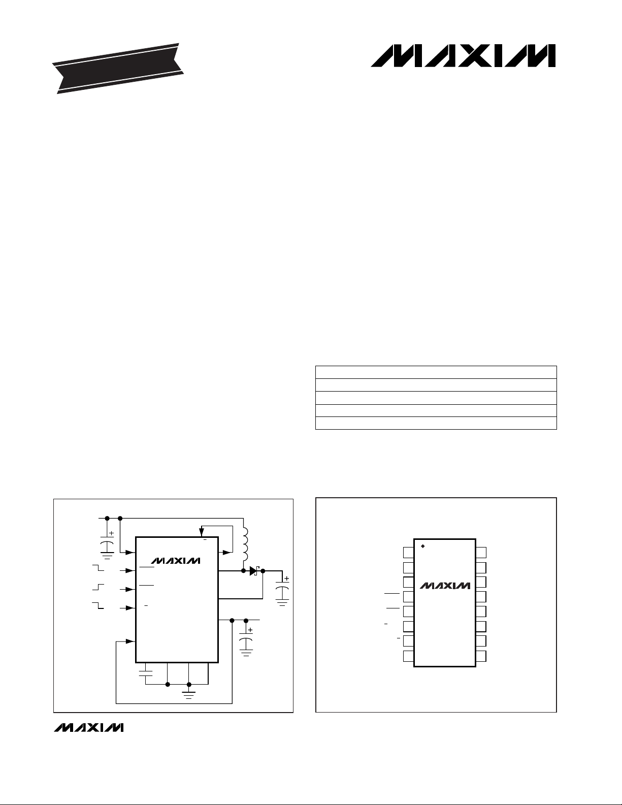
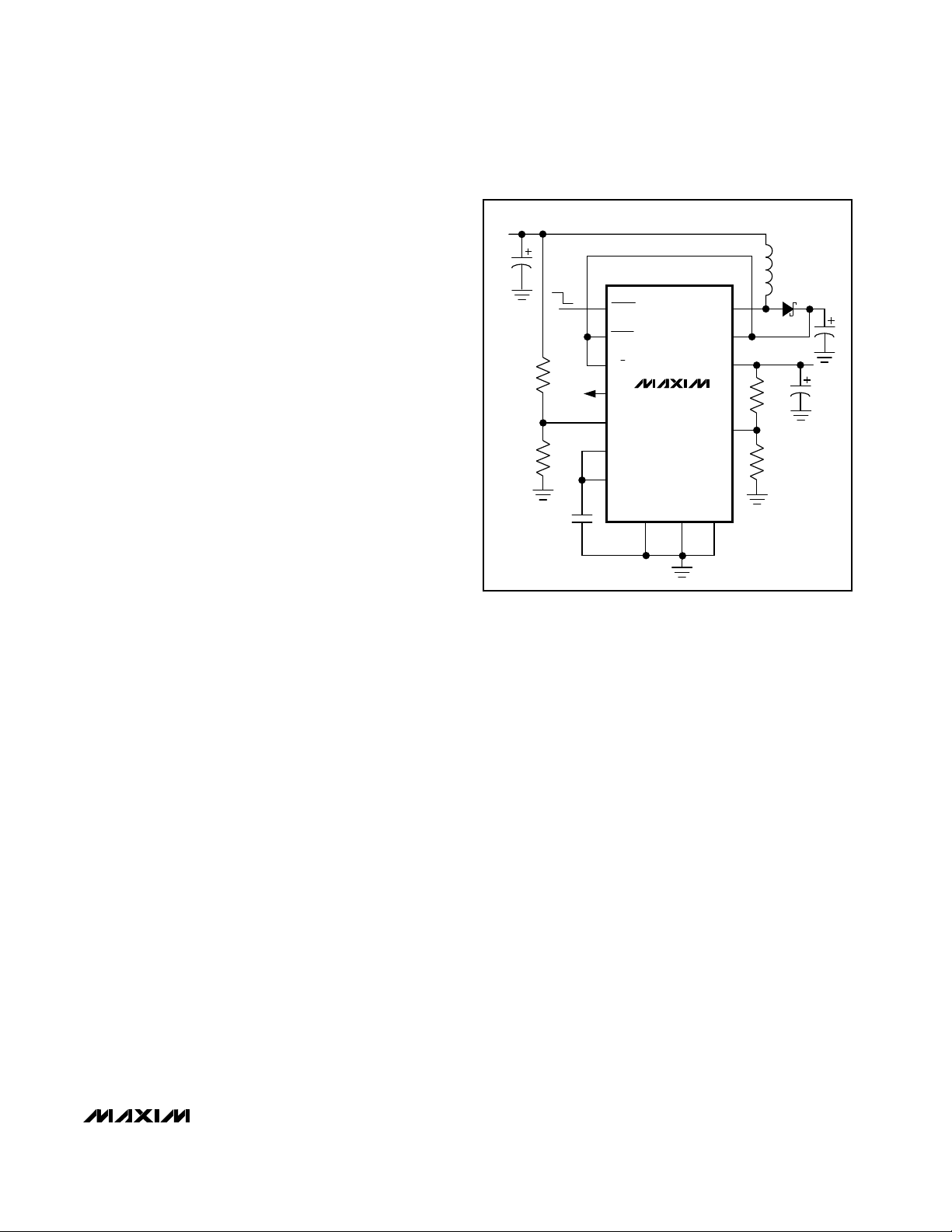
MAX710
LBI+ LBO
N/E
SHDN
OFF
ON
STBY
3/5
LBI-
REF PGND
C3
0.1µF
GND ILIM
LX
PS
C4
C1
C2
L1
OUTPUT
3.3V/5V
+1.8V TO +11V
INPUT
OUT
5V
3.3V
ON
STBY
__________Typical Operating Circuit
19-1254; Rev 0; 7/97
PART
MAX710C/D
MAX710ESE
MAX711C/D
0°C to +70°C
-40°C to +85°C
0°C to +70°C
TEMP. RANGE PIN-PACKAGE
Dice
16 Narrow SO
Dice
EVALUATION KIT MANUAL
FOLLOWS DATA SHEET
______________Ordering Information
MAX711ESE -40°C to +85°C 16 Narrow SO
For free samples & the latest literature: http://www.maxim-ic.com, or phone 1-800-998-8800.
For small orders, phone 408-737-7600 ext. 3468.
Page 2
MAX710/MAX711
3.3V/5V or Adjustable,
Step-Up/Down DC-DC Converters
2 _______________________________________________________________________________________
ABSOLUTE MAXIMUM RATINGS
ELECTRICAL CHARACTERISTICS
(VPS= 5.6V, STBY = PS, C
REF
= 0.1µF, C
OUT
= 4.7µF, TA= -40°C to +85°C, unless otherwise noted. Typical values are at
T
A
= +25°C.) (Note 1)
Stresses beyond those listed under “Absolute Maximum Ratings” may cause permanent damage to the device. These are stress ratings only, and functional
operation of the device at these or any other conditions beyond those indicated in the operational sections of the specifications is not implied. Exposure to
absolute maximum rating conditions for extended periods may affect device reliability.
PS, LX, OUT to GND............................................-0.3V to +11.5V
ILIM, SHDN, STBY, FB, 3/5, N/E, LBO,
LBI-, LBI+, REF to GND...........................-0.3V to (V
PS
+ 0.3V)
PGND to GND .......................................................-0.3V to +0.3V
REF Short Circuit to GND...........................................Continuous
I
OUT
...................................................................................700mA
Continuous Power Dissipation (T
A
= +70°C)
SO (derate 8.70mW/°C above +70°C)..........................696mW
Operating Temperature Range ...........................-40°C to +85°C
Storage Temperature Range.............................-65°C to +160°C
Junction Temperature......................................................+150°C
Lead Temperature (soldering, 10sec).............................+300°C
ILIM = GND
ILIM = PS
VLX= 5.6V
MAX711, VPS= 2.7V
MAX710, VPS= 3.7V
V
STBY
= 0V, linear regulator
VPS= 5.6V
FB = 1.25V
TA= -40°C to +85°C, I
REF
= 0
TA= 0°C to +85°C, I
REF
= 0
MAX711
V
STBY
= V
SHDN
= logic high, current measured
into PS pin; I
LOAD
= 0
V
STBY
= 0V
V
SHDN
= 0V
MAX711, OUT = FB
CONDITIONS
A
1.1 1.5 1.95
LX Current Limit
0.5 0.8 1.3
µA0.1 1LX Leakage Current
Ω
0.6 1.2
LX On-Resistance 0.3 0.9
0.2 0.6
nA1 50FB Input Current
mV
1.18 1.25 1.31
FB Voltage
V0.9Full Load Start-Up Voltage
1.20 1.25 1.29
mA10Standby Output Current
V
1.23 1.28 1.32
Reference Voltage
1.24 1.28 1.31
VFB 5.5Output Voltage-Adjustment Range
µA100 140Quiescent Current
µA7 16Standby Quiescent Current
µA0.1 5Shutdown Quiescent Current
UNITSMIN TYP MAXPARAMETER
TA= 0°C to +85°C
TA= -40°C to +85°C
0mA ≤ I
LOAD
≤ 250mA
MAX711, OUT = FB %0.1 1Load Regulation
3/5 = low,
I
OUT
= 0 to 250mA
V
4.8 5.0 5.2TA= 0°C to +85°C
4.6 5.0 5.3TA= -40°C to +85°C
3/5 = high, I
OUT
= 0 to
250mA, V
PS
= 4.7V
3.17 3.3 3.43TA= 0°C to +85°C
3.05 3.3 3.55TA= -40°C to +85°C
Output Voltage (MAX710)
0 < I
OUT
< 250mA, STBY = PS
%0.5Output Voltage Load Regulation
STBY = PS, 1.8V to 5V
%/V0.3Output Voltage Line Regulation
N/E = GND (Note 2)
N/E = PS
V
1.8 7.0
1.8 11.0
Input Voltage
Page 3
MAX710/MAX711
3.3V/5V or Adjustable,
Step-Up/Down DC-DC Converters
_______________________________________________________________________________________ 3
ELECTRICAL CHARACTERISTICS (continued)
(VPS= 5.6V, STBY = PS, C
REF
= 0.1µF, C
OUT
= 4.7µF, TA= -40°C to +85°C, unless otherwise noted. Typical values are at
T
A
= +25°C.) (Note 1)
Note 1: Specifications at -40°C are guaranteed by design, not production tested.
Note 2: Guaranteed by design (see Table 1).
Note 3: The LBO comparator provides the correct result as long as one input is within the specified input range.
STBY, SHDN, N/E, 3/5, ILIM
STBY = PS
CONDITIONS
V0.4Input Low Voltage
°C150Thermal Shutdown
UNITSMIN TYP MAXPARAMETER
STBY, SHDN, N/E, 3/5, ILIM
STBY, SHDN, N/E, 3/5, ILIM
(Note 3)
V
LBI-
, V
LBI+
= 1.25V
mV6 40 100Hysteresis
V1.6Input High Voltage
nA1 50Input Bias Current
V1.2 10Input Range LBI-, LBI+
nA1 50Input Bias Current LBI-, LBI+
V
LBI-
= 1.25V
I
LBO
= 2mA, V
LBI-
= 1.25V, V
LBI+
= 1V
I
LBO
= -300µA, V
LBI-
= 1.25V, V
LBI+
= 2V
mV-25 +25LBI/LBO Offset Voltage
0.4
V
VPS- 0.2V
LBO Output Voltage
V
OUT
= 5.0V
Ω
0.7 1.3
Output PFET Resistance
V
PS
= 3V, V
OUT
= 0V µA0.4 3Output PFET Leakage
MAX711, V
OUT
= 2.7V 1.6 3.0
MAX710, V
OUT
= 3.0V 1.3 2.4
STBY = PS
°C20Thermal Shutdown Hysteresis
LOGIC
LBI/LBO COMPARATOR
Page 4
__________________________________________Typical Operating Characteristics
(TA = +25°C, unless otherwise noted.)
MAX710/MAX711
3.3V/5V or Adjustable,
Step-Up/Down DC-DC Converters
4 _______________________________________________________________________________________
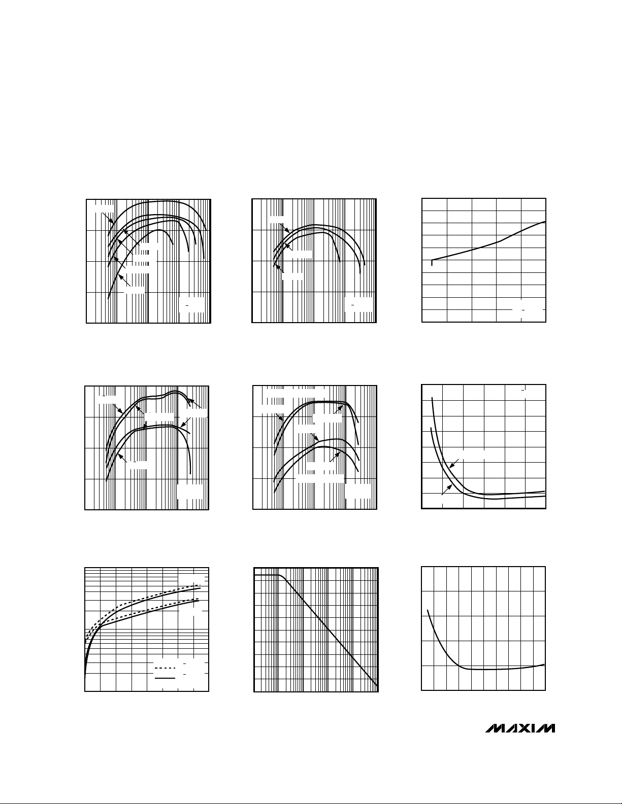
90
50
0.1 10 10001 100
EFFICIENCY vs. LOAD CURRENT—
HIGH-EFFICIENCY AND LOW-NOISE MODES
(V
OUT
= 5V)
60
MAX710/711 TOC04
LOAD CURRENT (mA)
EFFICIENCY (%)
70
80
V
OUT
= 5V
V
IN
= 2.5V
N/E = GND
N/E = PS
ILIM = 0.8A
ILIM = 1.5A
60
10
0.01 101 10000.1 100
LINEAR-REGULATOR POWER-SUPPLY
REJECTION RATIO vs. FREQUENCY
20
MAX710/711 TOC08
FREQUENCY (kHz)
PSRR (dB)
30
40
50
55
15
25
35
45
90
50
0.1 10 10001 100
EFFICIENCY vs. LOAD CURRENT—
HIGH-EFFICIENCY AND LOW-NOISE MODES
(V
OUT
= 3.3V)
60
MAX710/711 TOC05
LOAD CURRENT (mA)
EFFICIENCY (%)
70
80
V
OUT
= 3.3V
V
IN
= 2.5V
ILIM = 0.8A
ILIM = 0.8A
ILIM = 1.5A
LOW-NOISE MODE
HIGH-EFFICIENCY MODE
ILIM = 1.5A
0
200
600
800
400
1200
1400
1000
1600
0 42 6 8 10 12
NO-LOAD BATTERY CURRENT
vs. INPUT VOLTAGE
MAX710/711 TOC06
INPUT VOLTAGE (V)
SUPPLY CURRENT (µA)
N/E = GND
ILIM = GND (1.5A)
ILIM = PS (0.8A)
0
0.2
0.6
0.4
0.8
1.0
1 3 4 52 6 87 9 10 11
SHUTDOWN CURRENT
vs. INPUT VOLTAGE
MAX710/711 TOC09
INPUT VOLTAGE (V)
SHUTDOWN CURRENT (µA)
1000
10
1.0 1.4 2.2 2.6
MAXIMUM OUTPUT CURRENT
vs. INPUT VOLTAGE
100
MAX710/711 TOC07
INPUT VOLTAGE (V)
MAXIMUM OUTPUT CURRENT (mA)
1.81.2 2.01.6 2.4
ILIM = GND
ILIM = PS
N/E = GND
N/E = PS
90
50
0.1 10 10001 100
EFFICIENCY vs. OUTPUT CURRENT—
HIGH-EFFICIENCY MODE
(V
OUT
= 5V)
60
MAX710/711 TOC01
OUTPUT CURRENT (mA)
EFFICIENCY (%)
70
80
VIN = 1V
V
OUT
= 5V
N/E = GND
VIN = 3.6V
VIN = 2.5V
VIN = 5.6V
VIN = 1.8V
90
50
0.1 10 10001 100
EFFICIENCY vs. OUTPUT CURRENT—
HIGH-EFFICIENCY MODE
(V
OUT
= 3.3V)
60
MAX710/711 TOC02
OUTPUT CURRENT (mA)
EFFICIENCY (%)
70
80
V
OUT
= 3.3V
N/E = GND
VIN = 2.5V
VIN = 1V
VIN = 1.8V
0
0.6
0.4
0.2
0.8
1.0
1.2
1.4
1.6
1.8
2.0
0 10050 150 200 250
MINIMUM START-UP INPUT VOLTAGE
vs. LOAD CURRENT
MAX710/711 TOC03
LOAD CURRENT (mA)
INPUT VOLTAGE (V)
V
OUT
= 5V
N/E = PS
Page 5

MAX710/MAX711
3.3V/5V or Adjustable,
Step-Up/Down DC-DC Converters
_______________________________________________________________________________________
5
LINE-TRANSIENT RESPONSE
A
B
MAX710/711 TOC10
A: V
OUT
= 3.3V (100mV/div, AC COUPLED), N/E = GND
B: V
IN
= 2V TO 4V, I
OUT
= 100mA
2ms/div
A: V
OUT
= 3.3V (50mV/div, AC COUPLED), N/E = PS
B: I
OUT
= 10mA TO 100mA
LOAD-TRANSIENT RESPONSE
A
B
MAX710/711 TOC11
1ms/div
VIN = 2.5V, I
OUT
= 20mA, N/E = GND
V
OUT
= 5V (20mV/div, AC COUPLED), I
OUT
= 20mA
200µs/div
OUTPUT RIPPLE (HIGH-EFFICIENCY MODE)
MAX710/711 TOC12
VIN = 2.5V, I
OUT
= 20mA, N/E = PS
V
OUT
= 5V (20mV/div, AC COUPLED), I
OUT
= 20mA
OUTPUT RIPPLE (LOW-NOISE MODE)
MAX710/711 TOC13
200µs/div
A: V
OUT
(2V/div), I
OUT
= 100mA
B: V
SHDN
(2V/div)
START-UP DELAY
A
B
MAX710/711 TOC14
20µs/div
A: V
OUT
(2V/div), I
OUT
= 100mA
B: V
SHDN
(2V/div)
TURN-OFF DELAY
A
B
MAX710/711 TOC15
200µs/div
____________________________Typical Operating Characteristics (continued)
(TA = +25°C, unless otherwise noted.)
Page 6
_______________Detailed Description
The MAX710/MAX711 integrate a step-up DC-DC converter with a linear regulator to provide step-up/down
voltage conversion. The step-up switch-mode regulator
contains an N-channel power MOSFET switch. It also
shares a precision voltage reference with a linear regulator that contains a P-channel MOSFET pass element
(Figure 1).
Step-Up Operation
A pulse-frequency-modulation (PFM) control scheme
with a constant 1µs off-time and variable on-time controls the N-channel MOSFET switch. The N-channel
switch turns off when the part reaches the peak current
limit or the 4µs maximum on-time. The ripple frequency
is a function of load current and input voltage.
Step-Down Operation
The low-dropout linear regulator consists of a reference, an error amplifier, and a P-channel MOSFET. The
reference is connected to the error amplifier’s inverting
input. The error amplifier compares this reference with
the selected feedback voltage and amplifies the difference. The difference is conditioned and applied to the
P-channel pass transistor’s gate.
Operating Configurations
The MAX710/MAX711 have several operating configurations to minimize noise and optimize efficiency for different input voltage ranges. These configurations are
accomplished via the N/E input, which controls operation of the on-chip linear regulator.
With N/E low, the linear regulator behaves as a 0.7Ω (at
5V output) PFET switch when the IC is boosting, and as
a conventional linear regulator when VIN> V
OUT
. This
provides optimum boost efficiency, but the PFET does
little to reject boost-converter output ripple. With N/E
high, boost ripple rejection is optimized by maintaining
headroom (VFV, typically 0.5V at 5V output) across the
linear regulator. Boost mode efficiency is then about
10% lower than with N/E high.
MAX710/MAX711
3.3V/5V or Adjustable,
Step-Up/Down DC-DC Converters
6 _______________________________________________________________________________________
______________________________________________________________Pin Description
Drain Connection for internal N-channel power MOSFETLX1
Power GroundPGND2
Shutdown Input. When low, the entire circuit is off and OUT is actively pulled to GND.
SHDN
4
Inductor Current-Limit-Select Input. Connect to GND for 1.5A limit and to PS for 0.8A limit.ILIM3
Standby Input. Connect to GND to disable boost circuit. Connect to PS for normal operation.
STBY
5
Selects low-noise or high-efficiency mode. Connect to GND for high efficiency and to PS for
lowest noise. See
Operating Configurations
section.
N/E
7
Selects the output voltage. Connect to GND for 5V output and to OUT for 3.3V output.
3/5
6
2
4
3
5
7
—
1
Low-Battery Comparator OutputLBO8 8
Negative Input to Low-Battery ComparatorLBI-10
Source of internal PFET regulator. The IC is powered from PS.PS12
Positive Input to Low-Battery ComparatorLBI+11
1.28V Reference Voltage Output. Bypass with a 0.1µF capacitor to GND.REF13
Power GroundPGND15
Analog Ground. Must be low impedance. Solder directly to ground plane.GND14
10
12
11
13
15
14
9
Drain Connection for internal N-channel power MOSFETLX16 16
Linear-Regulator Output. Bypass with a 4.7µF capacitor to GND.OUT9
MAX711MAX710
FUNCTIONNAME
PIN
Feedback InputFB— 6
Page 7

MAX710/MAX711
3.3V/5V or Adjustable,
Step-Up/Down DC-DC Converters
_______________________________________________________________________________________ 7
∆t
ON
FIXED t
OFF
GENERATOR
DRV
PS
N/E
PS
OFF
REF2
REF1
CURRENTLIMIT COMPARATOR
100mV
V
OUT
ERROR
AMP2
ERROR
AMP1
REF1
V
FV
LX
ILIM
V
IN
PGND
PGND
PS
OUT
(FB)
3.3/5
GND
REFB
N
REFA
LBI-
LBI+
STBY
REF
SHDN
LBO
( ) IS FOR MAX711.
REF2
REF1
MAX710
Figure 1. Functional Diagram
Page 8

MAX710/MAX711
3.3V/5V or Adjustable,
Step-Up/Down DC-DC Converters
8 _______________________________________________________________________________________
MAX710
SHDN LX
STBY
N/E
LBO
LBI+
LBI-
REF
PGND
0.1µF
GND ILIM
PS
OUT
4.7µF
100µF
V
IN
= +1.8V TO +11V
100µF
L1
3/5
Figure 2a. High-Efficiency Operating Configuration for
V
BATT
< V
OUT
Figure 2b. High-Efficiency Operating Configuration for
V
BATT
< 6.5V
In high-efficiency mode (N/E = low), the maximum
input voltage is limited to 7V. This voltage limitation is
easily overcome, however, by configuring the LBO output to change modes based on input voltage, allowing
an 11V maximum input with high-efficiency configurations. Four operating configurations are described in
Table 1 and in the following subsections.
Configuration 1: High Efficiency, 7V Max V
IN
With N/E connected to GND, when the IC boosts, the
linear regulator operates only as a switch, with minimum forward drop, until VIN> V
OUT
(where linear regulation begins). This configuration is limited to no more
than 7V input, but provides best efficiency for batteryonly operation or low-voltage AC adapter usage.
Configuration 2: High Efficiency, V
BATT
< V
OUT
In this configuration, N/E is driven high by LBO when
VIN> V
OUT
(Figure 2a). When VIN< V
OUT
, the IC
boosts, and the linear regulator operates as a switch,
with minimum forward drop. When VIN> V
OUT
, the linear regulator operates with VFVforward drop, while V
PS
increases by VFVso that OUT maintains regulation. V
FV
is set inside the IC to approximately 0.5V (at 5V V
OUT
).
When VINis only slightly higher than V
OUT
, conversion
efficiency is poorer than in configuration 1, so configuration 2 is most suitable when the battery voltage is less
than V
OUT
, but the AC adapter output is greater than
V
OUT
.
Up to 11V2
Up to 11V4
Up to 11V3
High efficiency,
V
BATT
< V
OUT
(Figure 2a)
Low noise
High efficiency,
11V, V
BATT
< 6.5V
(Figure 2b)
DESCRIPTION
High efficiency,
7V max V
IN
INPUT
VOLTAGE
Up to 7V1
NO.
LBO = N/E
LBI- = V
OUT
LBI+ = V
IN
N/E = PS
LBO = N/E
LBI- = REF
LBI+ = R5, R6
CONNECTIONS
N/E = GND
Table 1. Operating Configurations
= +1.8V TO +11V
V
IN
100µF
SHDN LX
STBY
N/E
LBO
LBI+
LBI-
REF
MAX710
PGND
R5
R6
0.1µF
OUT
GND ILIM
3/5
L1
4.7µF
(V
REF
= 6.5V
IN
- V
IN
REF
= 1.28V
100µF
)
REF
PS
R5 = R6
V
R5 = R6 (4.08)
WHEN V
AND V
Page 9
MAX710/MAX711
3.3V/5V or Adjustable,
Step-Up/Down DC-DC Converters
_______________________________________________________________________________________ 9
Configuration 3: High Efficiency, 11V, V
BATT
< 6.5V
In this configuration, N/E is driven high by LBO when
VIN> 6.5V (Figure 2b). When VIN< V
OUT
, the IC
boosts, and the linear regulator operates as a switch,
with minimum forward drop. When VIN> V
OUT
, linear
regulation begins. When VIN> 6.5V (set by R5 and R6),
the linear regulator forces a minimum forward drop of
VFV(typically 0.5V at 5V V
OUT
) as LBO drives N/E high.
This transition is not seen at the output, since the linear
regulator already has an input-output voltage difference
of 6.5V - 5V. Efficiency with VINslightly higher than
V
OUT
is equal to that of configuration 1, so configuration 3 is most suitable when the battery voltage may be
near V
OUT
. This hookup has no functional shortcomings
compared with configuration 2, except that two additional resistors (R5 and R6) are needed.
Configuration 4: Low Noise
With N/E connected to PS, when the IC is boosting, the
linear regulator operates with VFVforward voltage (typically 0.5V at 5V V
OUT
) for optimum noise rejection.
Linear regulation occurs when VIN> V
OUT
+ VFV. The
VFVvoltage differential results in boost efficiency typically 10% lower than with the high-efficiency configurations.
ILIM
The current-limit-select input, ILIM, selects between the
two peak current limits: 1.5A (ILIM = GND) and 0.8A
(ILIM = PS). If the application requires 200mA or less
from the MAX710/MAX711, select 0.8A. The lower peak
current limit permits the use of smaller, low-cost inductors. The ILIM input is internally diode clamped to GND
and PS, and should not be connected to signals outside this range.
Shutdown and Standby Modes
Grounding SHDN turns off the MAX710/MAX711 completely, disconnecting the input from the output. Tie
SHDN to PS for normal operation.
The MAX710/MAX711 have a standby mode that shuts
down the step-up converter. The linear regulator
remains on with a 7µA (typ) LDO quiescent current.
Connect STBY to ground to enter standby mode; other-
wise, connect STBY to PS.
__________________Design Procedure
Output Voltage Selection
For the MAX710, you can obtain a 3.3V or 5V output
voltage by tying 3/5 to GND or PS. Efficiency is typically
85% over a 2mA to 250mA load range. The device is
bootstrapped, with power derived from the step-up
voltage output (at PS). Under all load conditions, the
MAX710/MAX711 typically start up with a 1V input. If
the battery voltage exceeds the programmed output
voltage, the output will linear regulate down to the
selected output voltage.
The MAX711’s adjustable output voltage is set by two
resistors, R1 and R2 (Figure 3), which form a voltage
divider between the output and FB. Use the following
equation to determine the resistor values:
R1 = R2 [(V
OUT
/ V
REF
) - 1]
where V
REF
= 1.25V.
Since the input bias current at FB has a maximum value
of 50nA, R1 and R2 can be large with no significant
accuracy loss. Choose R2 in the 100kΩ to 1MΩ range
and calculate R1 using the formula above. For 1%
error, the current through R1 should be at least 100
times FB’s bias current.
Low-Battery Comparator
The MAX710/MAX711 contain a comparator for lowbattery detection. If the voltage at LBI+ falls below that
at LBI- (typically connected to REF), LBO goes low.
Hysteresis is typically 50mV. Set the low-battery monitor’s threshold with two resistors, R3 and R4 (Figure 2),
using the following equation:
R3 = R4 [(V
LBT
/ V
LBI
-) - 1]
MAX711
SHDN LX
STBY
N/E
LBO
LBI+
LBI-
REF
PGND GND ILIM
PS
OUT
R4
R3
R2
R1
C4
C1
IN
C2
L1
FB
OFF
ON
Figure 3. MAX711 Adjustable Output Voltage
Page 10

MAX710/MAX711
3.3V/5V or Adjustable,
Step-Up/Down DC-DC Converters
10 ______________________________________________________________________________________
where V
LBT
is the desired threshold of the low-battery
detector and V
LBI-
is the voltage applied to the inverting input of the low-battery comparator. Since LBI current is less than 50nA, R3 and R4 can be large
(typically 100kΩ to 1MΩ), minimizing input supply loading. If the low-battery comparator is not used, connect
LBI+ to PS and LBI- to REF, leaving LBO unconnected.
Inductor Selection
A 22µH inductor value performs well in most
MAX710/MAX711 applications. The inductance value is
not critical, however, since the MAX710/MAX711 work
with inductors in the 18µH to 100µH range. Smaller
inductance values typically offer a smaller size for a
given series resistance, allowing the smallest overall
circuit dimensions. Circuits using larger inductance values exhibit higher output current capability and larger
physical dimensions for a given series resistance. The
inductor’s incremental saturation current rating should
be greater than the peak switch-current limit, which is
1.5A for ILIM = GND and 0.8A for ILIM = PS. However,
it is generally acceptable to bias most inductors into
saturation by as much as 20%, although this slightly
reduces efficiency. The inductor’s DC resistance significantly affects efficiency. See Tables 2 and 3 for a list of
suggested inductors and suppliers.
Capacitor Selection
A 100µF, 16V, 0.1Ω equivalent series resistance (ESR),
surface-mount tantalum (SMT) output filter capacitor,
C2, typically exhibits 50mV output ripple when stepping
up from 2V to 5V at 100mA. Smaller capacitors (down
to 10µF with higher ESRs) are acceptable for light loads
or in applications that can tolerate higher output ripple.
The ESR of both bypass and filter capacitors affects
efficiency and output ripple. Output voltage ripple is the
product of the peak inductor current and the output
capacitor’s ESR. Use low-ESR capacitors for best performance, or connect two or more filter capacitors in
parallel. Low-ESR, SMT capacitors are currently available from Sprague (595D series) and AVX (TPS series).
Sanyo OS-CON organic-semiconductor through-hole
capacitors also exhibit very low ESR and are especially
useful for operation at cold temperatures. The output
capacitor, C3, needs to be only 4.7µF to maintain linear
regulator stability. See Tables 2 and 3 for a list of suggested capacitors and suppliers.
Rectifier Diode
For optimum performance, use a switching Schottky
diode. Refer to Tables 2 and 3 for the suggested diode
and supplier.
__________Applications Information
The MAX710/MAX711 high-frequency operation makes
PC layout important for minimizing ground bounce and
noise. Keep the IC’s GND pin and the ground leads of
C1 and C2 (Figure 1) less than 0.2in. (5mm) apart. Also
keep all connections to the FB and LX pins as short as
possible. To maximize output power and efficiency and
minimize output ripple voltage, use a ground plane and
solder the IC’s GND pin directly to the ground plane.
4.7µF, 16V tantalum capacitor
Sprague 595D475X0016A2T
RECTIFIERS (D1)
Schottky diode
Motorola MBRS130T3
Coilcraft DO33-08P-223
INDUCTORS (L1)
Sumida CD75-220 (1.5A),
CDRH-74-220 (1.23A), or
CD54-220
CAPACITORS
100µF, 16V low-ESR tantalum capacitor
AVX TPSE107M016R0100 or
Sprague 593D107X0016E2W
Table 2. Component Selection
Table 3. Component Suppliers
(803) 626-3123(803) 946-0690
FAX
AVX
SUPPLIER PHONE
(847) 639-1469(847) 639-6400Coilcraft
(602) 994-6430(602) 303-5454
(603) 224-1430(603) 224-1961Sprague
Motorola
(847) 956-0702(847) 956-0666Sumida
___________________Chip Information
TRANSISTOR COUNT: 661
SUBSTRATE CONNECTED TO GND
(619) 661-1055(619) 661-6835Sanyo
Page 11

MAX710/MAX711
3.3V/5V or Adjustable,
Step-Up/Down DC-DC Converters
______________________________________________________________________________________ 11
________________________________________________________Package Information
SOICN.EPS
Page 12

MAX710/MAX711
3.3V/5V or Adjustable,
Step-Up/Down DC-DC Converters
12 ______________________________________________________________________________________
NOTES
 Loading...