

Page 1
General Description
The MAX7058 UHF transmitter alternately transmits
ASK/OOK data at 315MHz or 390MHz using a single
crystal. The MAX7058 has internal tuning capacitors at
the output of the power amplifier that can be programmed for matching to the antenna or load. The
MAX7058 can transmit at a data rate up to 100kbps
NRZ (50kbps Manchester coded). Typical transmitted
power into a 50Ω load is +10dBm. The MAX7058 operates from +2.1V to +3.6V and draws under 8.0mA of
current. The standby current is less than 1µA at room
temperature. A 15MHz crystal is used as the reference
for 315MHz and 390MHz operation by selecting synthesizer-divide ratios of 21 and 26, respectively.
The MAX7058 is available in a 4mm x 4mm, 24-pin thin
QFN package and is specified to operate in the -40°C
to +125°C automotive temperature range.
Applications
Garage Door Openers
RF Remote Controls
Home Automation
Wireless Sensors
Security Systems
Automotive
Features
♦ Switched 315MHz/390MHz Carrier Frequency
Using One Crystal
♦ +2.1V to +3.6V Single-Supply Operation
♦ ASK/OOK Modulation
♦ Internal Switched Capacitors for Optimum Dual-
Frequency Operation
♦ 8.0mA DC Current Drain (50% Duty Cycle OOK)
♦ 0.8µA Standby Current
♦ Small 4mm x 4mm, 24-Pin Thin QFN Package
MAX7058
315MHz/390MHz Dual-Frequency
ASK Transmitter
________________________________________________________________
Maxim Integrated Products
1
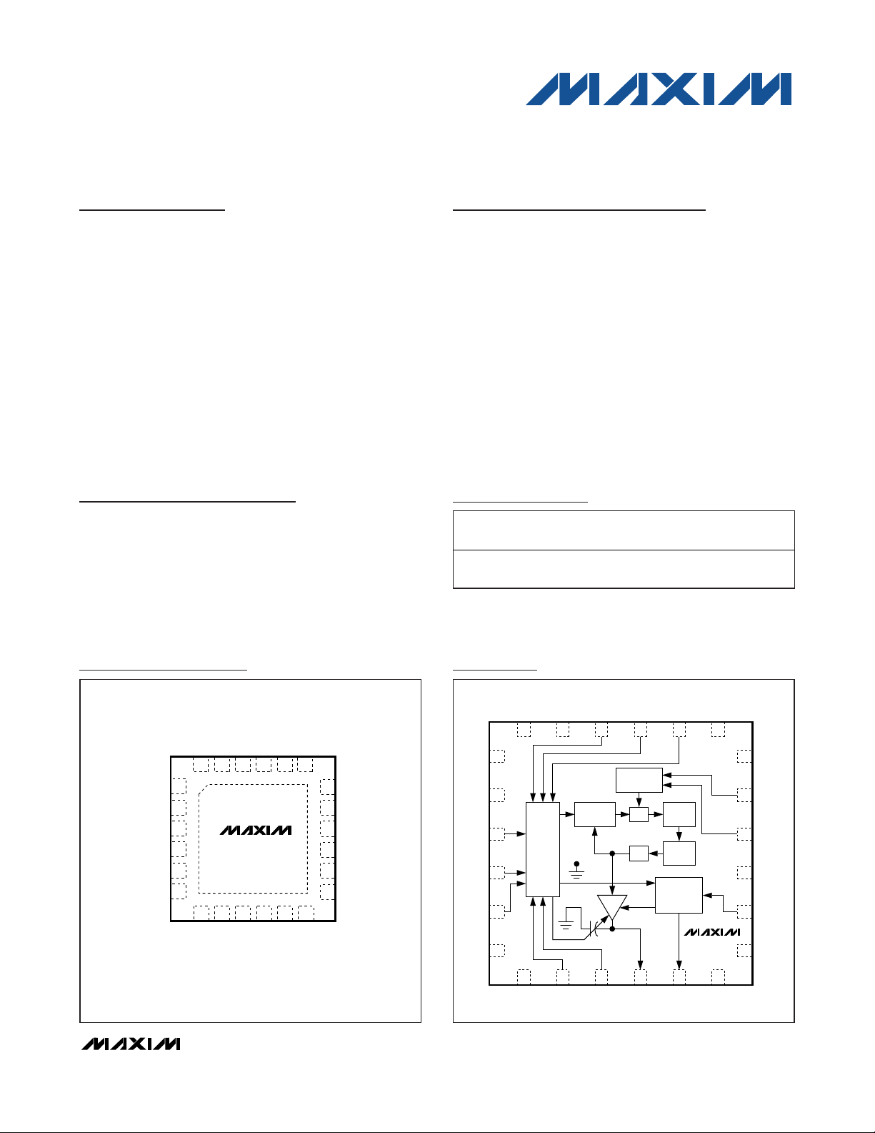
Pin Configuration
Ordering Information
5
6
4
3
14
13
15
CAP3
PAOUT
ROUT
N.C.
16
N.C.
N.C.
ENABLE
TOGGLE
N.C.
N.C.
78
CAP1
10 11 12
2324 22 20 19
CAP2
N.C.
XTAL2
AVDD
PAVDD
N.C.
MAX7058
CAP4
DIN
9
21
FSEL
2
17
XTAL1
DVDD
1
18
N.C.
N.C.
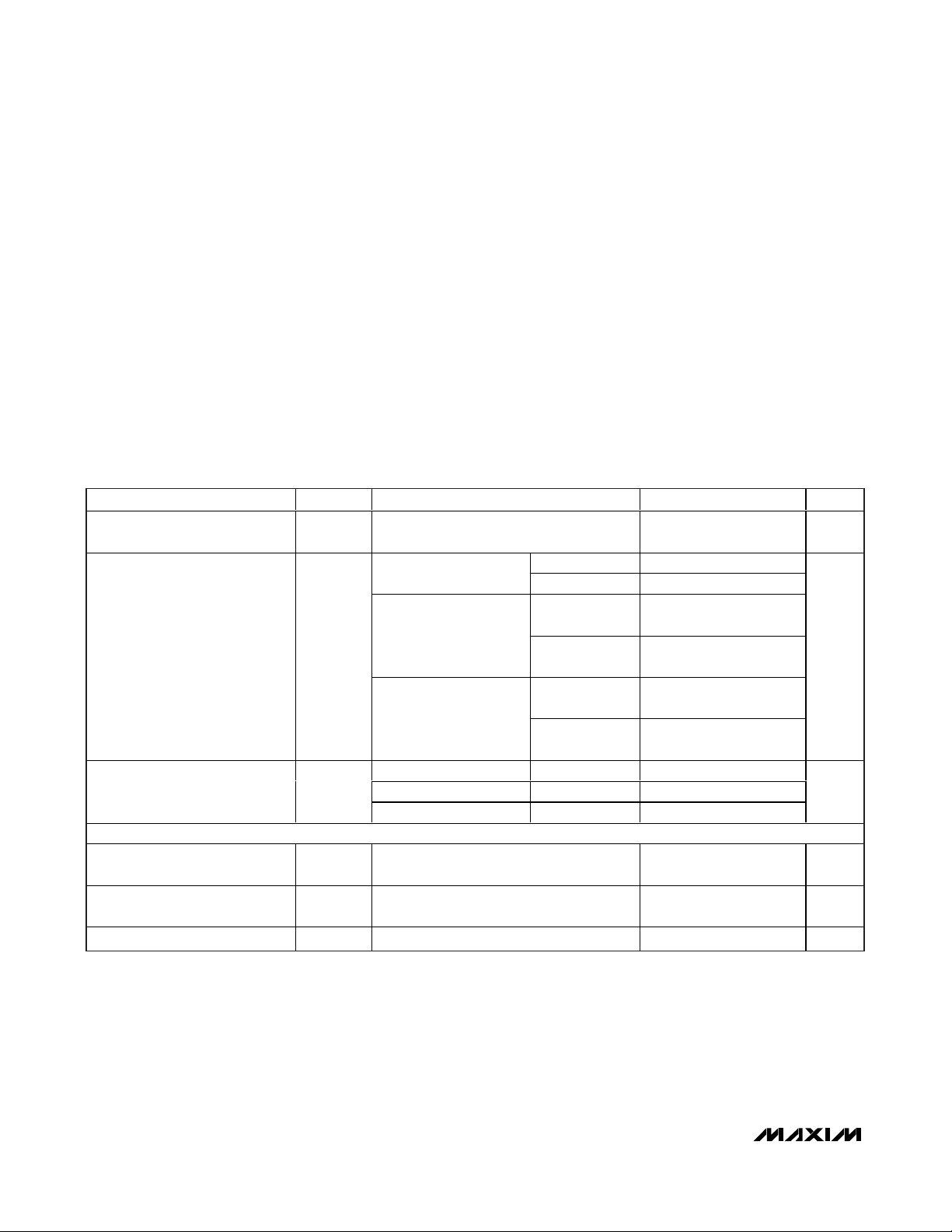
DIGITAL
CONTROL
FREQUENCY
÷21 OR ÷26
CRYSTAL
OSCILLATOR
CHARGE
PUMP
PFD
LOOP
FILTER
ENVELOPE
SHAPING
EXPOSED
PADDLE
(GND)
VCO
PA
MAX7058
1
2
3
4
78 910
TQFN
11 12
24 23 22 21 20 19
5
6
18
17
16
15
14
13
N.C.
FSEL
DVDD
CAP1
N.C.
N.C.
CAP3
CAP4
PAOUT
ROUT
N.C.
N.C.
N.C.
ENABLE
TOGGLE
N.C.
CAP2
N.C.
XTAL2
XTAL1
AVDD
N.C.
PAVDD
DIN
TOP VIEW
+
*EP = EXPOSED PADDLE.
EP*
Functional Block Diagram
19-3206; Rev 0; 1/08
For pricing, delivery, and ordering information, please contact Maxim Direct at 1-888-629-4642,
or visit Maxim’s website at www.maxim-ic.com.
+
Denotes a lead-free package.
*
EP = Exposed paddle.
PART TEMP RANGE PIN-PACKAGE
MAX7058ATG+ - 40°C to + 125°C
24 Thi n QFN - E P *
( 4m m x 4m m )
PKG
CODE
T2444+3
Page 2
MAX7058
315MHz/390MHz Dual-Frequency
ASK Transmitter
2 _______________________________________________________________________________________
ABSOLUTE MAXIMUM RATINGS
DC ELECTRICAL CHARACTERISTICS
(
Typical Operating Circuit
, 50Ω system impedance, AVDD = DVDD = PAVDD = +2.1V to +3.6V, fRF= 315MHz or 390MHz, TA=
-40°C to +125°C, unless otherwise noted. Typical values are at AVDD = DVDD = PAVDD = +2.7V, T
A
= +25°C, unless otherwise
noted. All min and max values are 100% tested at T
A
= +125°C, and guaranteed by design and characterization over temperature,
unless otherwise noted.)
Stresses beyond those listed under “Absolute Maximum Ratings” may cause permanent damage to the device. These are stress ratings only, and functional
operation of the device at these or any other conditions beyond those indicated in the operational sections of the specifications is not implied. Exposure to
absolute maximum rating conditions for extended periods may affect device reliability.
Supply Voltage, AVDD, DVDD, PAVDD to GND (Exposed
Paddle) ...................................………..……………-0.3V to +4V
All Other Pins ………..…Exposed Paddle - 0.3V to (VDD + 0.3V)
Continuous Power Dissipation (T
A
= +70°C)
24-Pin TQFN (derate 20.8mW/°C above +70°C) .....1666.7mW
Operating Temperature……………….………….-40°C to +125°C
Storage Temperature………………….……….…-65°C to +150°C
Lead Temperature (soldering, 10s) ......………………..…+300°C
PARAMETER SYMBOL CONDITIONS MIN TYP MAX UNITS
Supply Voltage V
DD
PAVDD, AVDD, and DVDD connected to
power supply, V
PA off, V
cycle
DIN
DD
at 0% duty
fRF = 315MHz 3.4 5.4
f
= 390MHz 3.8 6.3
RF
2.1 2.7 3.6 V
V
at 50%, duty cycle
DIN
IH
IL
(Notes 1, 2, 3)
V
at 100%, duty cycle
DIN
(Note 1)
V
(Note 3) TA < +85°C 1.0 4.0Standby Current I
ENABLE
< V
IL
Supply Current I
DIGITAL I/O
Input High Threshold V
Input Low Threshold V
Pulldown Sink Current 13 µA
DD
STDBY
fRF = 315MHz 8.0 13.7
f
= 390MHz 8.3 14.2
RF
fRF = 315MHz 12.6 21.9
f
= 390MHz 12.9 22.1
RF
TA = +25°C 0.8
TA < +125°C 6.2 16.1
0.9 x
DV
DD
0.1 x
DV
mA
µA
DD
V
V
Page 3
MAX7058
315MHz/390MHz Dual-Frequency
ASK Transmitter
_______________________________________________________________________________________ 3
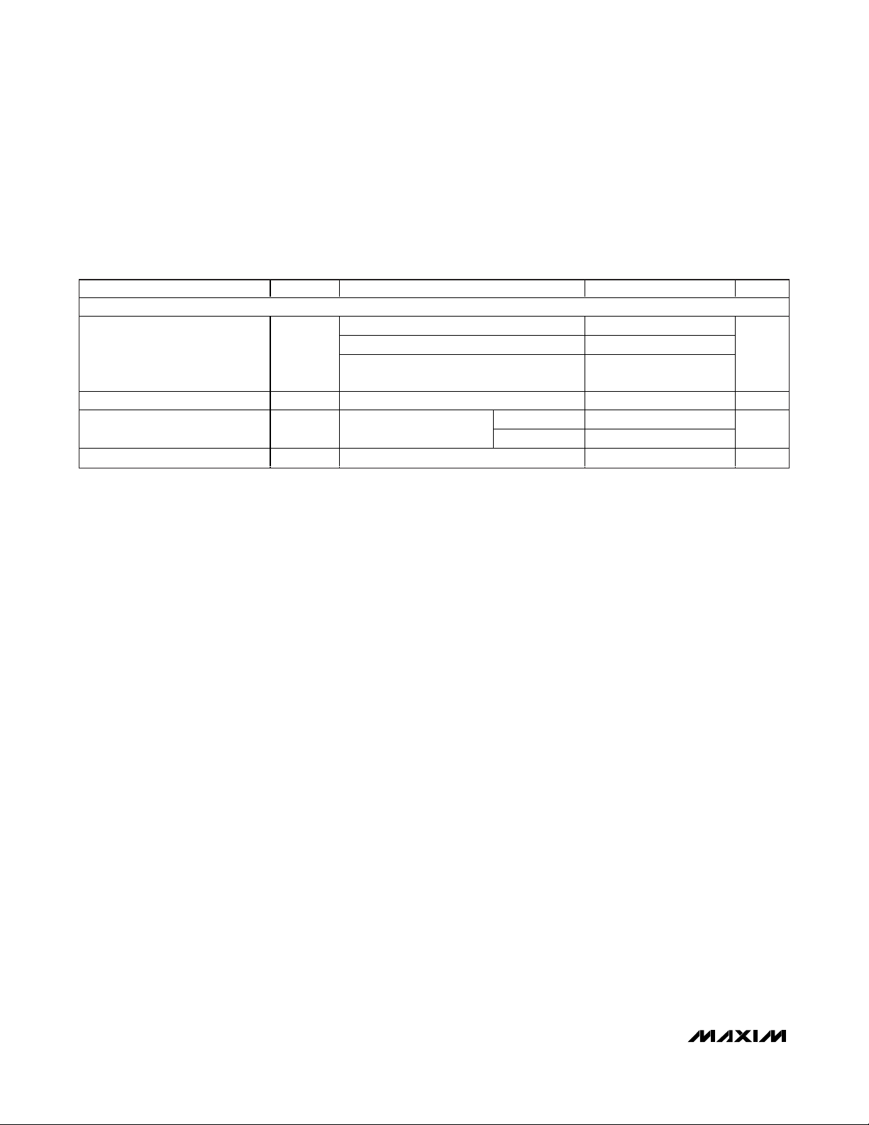
AC ELECTRICAL CHARACTERISTICS
(
Typical Operating Circuit
, 50Ω system impedance, AVDD = DVDD = PAVDD = +2.1V to +3.6V, fRF= 315MHz or 390MHz, TA=
-40°C to +125°C, unless otherwise noted. Typical values are at AVDD = DVDD = PAVDD = +2.7V, T
A
= +25°C, unless otherwise
noted. All min and max values are 100% tested at T
A
= +125°C, and guaranteed by design and characterization over temperature,
unless otherwise noted.)
PARAMETER SYMBOL CONDITIONS MIN TYP MAX UNITS
GENERAL CHARACTERISTICS
Frequency Range 300 315/390 450 MHz
Power-On Time t
Maximum Data Rate
Frequency Switching Time
PHASE-LOCKED LOOP (PLL)
VCO Gain K
PLL Phase Noise
Loop Bandwidth 600 kHz
Reference Frequency Input Level 500 mV
Fr eq uency- D i vi d er Rang e 21 26
CRYSTAL OSCILLATOR
Crystal Frequency f
Frequency Pulling by V
C r ystal Load C ap aci tance (Note 4) 10 pF
ENABLE transition low-to-high, frequency
ON
VCO
XTAL
DD
settled to within 50kHz of the desired carrier
ENABLE transition low-to-high, frequency
settled to within 5kHz of the desired carrier
Manchester encoded 50
Nonreturn to zero (NRZ) 100
Time from low-to-high or high-to-low
transition of FSEL to frequency settled to
within 5kHz of the desired carrier
fRF = 315MHz
f
= 390MHz
RF
10kHz offset -87
1MHz offset -98
10kHz offset -84
1MHz offset -98
110
250
30 µs
320 MHz/V
dBc/Hz
15 MHz
4 ppm/V
µs
kbps
P-P
Page 4
MAX7058
315MHz/390MHz Dual-Frequency
ASK Transmitter
4 _______________________________________________________________________________________
AC ELECTRICAL CHARACTERISTICS (continued)
(
Typical Operating Circuit
, 50Ω system impedance, AVDD = DVDD = PAVDD = +2.1V to +3.6V, fRF= 315MHz or 390MHz, TA=
-40°C to +125°C, unless otherwise noted. Typical values are at AVDD = DVDD = PAVDD = +2.7V, T
A
= +25°C, unless otherwise
noted. All min and max values are 100% tested at T
A
= +125°C, and guaranteed by design and characterization over temperature,
unless otherwise noted.)
Note 1: Supply current and output power are greatly dependent on board layout and PAOUT match.
Note 2: 50% duty cycle at 10kHz ASK data (Manchester coded).
Note 3: Guaranteed by design and characterization, not production tested.
Note 4: Dependent on PCB trace capacitance.
PARAMETER SYMBOL CONDITIONS MIN TYP MAX UNITS
POWER AMPLIFIER
Output Power (Note 1) P
Modulation Depth 80 dB
Maximum Carrier Harmonics
Reference Spur -48 dBc
TA = +25°C (Note 3) 4.2 10 15.5
OUT
TA = +125°C , P AV DD = AVD D = D VD D = +2.1V 3.0 5.9
TA = - 40°C , P AV D D = AV D D = D V D D = + 3.6V
( N ote 3)
With output matching
network
fRF = 315MHz -28
f
= 390MHz -32
RF
13.3 16.4
dBm
dBc
Page 5
MAX7058
315MHz/390MHz Dual-Frequency
ASK Transmitter
_______________________________________________________________________________________
5
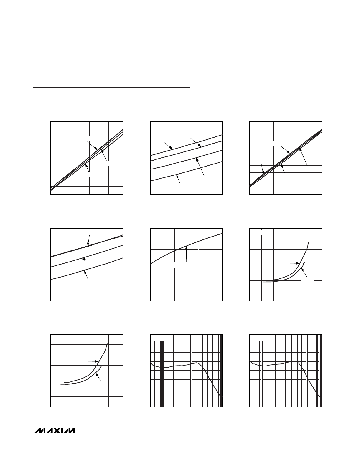
Typical Operating Characteristics
(TA = +25°C, unless otherwise noted.)
SUPPLY CURRENT
vs. SUPPLY VOLTAGE
18
fRF = 315MHz
17
PA ON
16
15
14
13
12
SUPPLY CURRENT (mA)
11
10
9
2.1
TA = +85°C and +125°C
TA = +25°C
TA = -40°C
SUPPLY VOLTAGE (V)
SUPPLY CURRENT
vs. SUPPLY VOLTAGE
5.0
fRF = 390MHz
PA OFF
4.5
4.0
3.5
3.0
SUPPLY CURRENT (mA)
2.5
2.0
2.1
TA = +85°C and +125°C
TA = +25°C
TA = -40°C
SUPPLY VOLTAGE (V)
SUPPLY CURRENT
vs. SUPPLY VOLTAGE
5.0
fRF = 315MHz
PA OFF
4.5
MAX7058 toc01
3.53.32.9 3.12.5 2.72.3
TA = +125°C
4.0
3.5
3.0
SUPPLY CURRENT (mA)
2.5
2.0
2.1
TA = +85°C
TA = +25°C
TA = -40°C
3.63.12.6
SUPPLY VOLTAGE (V)
19
18
MAX7058 toc02
17
16
15
14
13
12
SUPPLY CURRENT (mA)
11
10
9
2.1
OUTPUT POWER
vs. SUPPLY VOLTAGE
14
12
MAX7058 toc05
10
8
6
SUPPLY CURRENT (mA)
4
2
0
-40
MAX7058 toc04
3.63.12.6
14
12
10
8
6
OUTPUT POWER (dBm)
4
2
0
2.1
315MHz AND 390MHz
3.63.12.6
SUPPLY VOLTAGE (V)
SUPPLY CURRENT
vs. SUPPLY VOLTAGE
fRF = 390MHz
PA ON
TA = +125°C
TA = +85°C
SUPPLY VOLTAGE (V)
SUPPLY CURRENT
vs. OUTPUT POWER
315MHz
OUTPUT POWER (dBm)
MAX7058 toc03
TA = +25°C
TA = -40°C
3.63.12.6
MAX7058 toc06
ON
50% PA
20010-10-20-30
14
vs. OUTPUT POWER
390MHz
12
10
8
6
SUPPLY CURRENT (mA)
4
2
0
-30
SUPPLY CURRENT
ON
50% PA
OUTPUT POWER (dBm)
MAX7058 toc07
20100-10-20
-50
vs. OFFSET FREQUENCY
315MHz
-60
-70
-80
-90
-100
PHASE NOISE (dBc/Hz)
-110
-120
-130
100
PHASE NOISE
OFFSET FREQUENCY (Hz)
MAX7058 toc08
10M1M100k10k1k
-50
390MHz
-60
-70
-80
-90
-100
PHASE NOISE (dBc/Hz)
-110
-120
-130
100
PHASE NOISE
vs. OFFSET FREQUENCY
OFFSET FREQUENCY (Hz)
MAX7058 toc09
10M1M100k10k1k
Page 6

MAX7058
315MHz/390MHz Dual-Frequency
ASK Transmitter
6 _______________________________________________________________________________________
Typical Operating Characteristics (continued)
(TA = +25°C, unless otherwise noted.)
REFERENCE SPUR MAGNITUDE
vs. SUPPLY VOLTAGE
MAX7058 toc10
SUPPLY VOLTAGE (V)
REFERENCE SPUR MAGNITUDE (dBc)
3.63.12.6
-49.5
-49.0
-48.0
-48.5
-47.5
-47.0
-46.5
-46.0
-45.5
-50.0
2.1
390MHz
315MHz
FREQUENCY STABILITY
vs. SUPPLY VOLTAGE
MAX7058 toc11
SUPPLY VOLTAGE (V)
FREQUENCY STABILITY (ppm)
3.63.12.6
-3
-2
-1
0
1
2
3
4
-4
2.1
390MHz
315MHz
EFFICIENCY
vs. SUPPLY VOLTAGE
MAX7058 toc12
SUPPLY VOLTAGE (V)
EFFICIENCY (%)
3.63.0 3.32.4 2.7
14
12
16
18
22
20
24
28
26
30
10
2.1
TA = -40°C
TA = +25°C
315MHz
50% DUTY CYCLE
TA = +125°C
TA = +85°C
EFFICIENCY
vs. SUPPLY VOLTAGE
MAX7058 toc13
SUPPLY VOLTAGE (V)
EFFICIENCY (%)
3.63.0 3.32.4 2.7
20
25
30
35
40
15
2.1
TA = -40°C
TA = +25°C
315MHz
PA ON
TA = +125°C
TA = +85°C
EFFICIENCY
vs. SUPPLY VOLTAGE
MAX7058 toc14
SUPPLY VOLTAGE (V)
EFFICIENCY (%)
3.63.0 3.32.4 2.7
14
12
16
18
22
20
24
26
10
2.1
TA = +25°C
390MHz
50% DUTY CYCLE
TA = +125°C
TA = +85°C
TA = -40°C
EFFICIENCY
vs. SUPPLY VOLTAGE
MAX7058 toc15
SUPPLY VOLTAGE (V)
EFFICIENCY (%)
3.63.0 3.32.4 2.7
19
17
23
21
25
29
27
31
33
15
2.1
TA = +25°C
390MHz
PA ON
TA = +125°C
TA = +85°C
TA = -40°C
Page 7

MAX7058
315MHz/390MHz Dual-Frequency
ASK Transmitter
_______________________________________________________________________________________
7
_______________________________________________________________________________________
7
Pin Description
PIN NAME FUNCTION
1, 6, 7, 12,
13, 18, 19,
24
2 DVDD
3 FSEL
4 CAP1
5 CAP2
8 CAP3
9 CAP4
10 PAOUT
11 ROUT
14 PAVDD
15 AVDD
16 XTAL2 Crystal Input 2. XTAL2 can be driven from an AC-coupled external reference.
17 XTAL1 Crystal Input 1. Bypass to GND if XTAL2 is driven from an AC-coupled external reference.
20 TOGGLE
21 ENABLE
22 DIN
23 N.C. No connection. Must remain unconnected.
— EP (GND)
N.C. No Connection. Internally not connected.
Digital Positive Supply Voltage. Bypass to GND with 0.1µF and 0.01µF capacitors placed as close to
the pin as possible.
Frequency Select. Internally pulled down to GND when the part is not in standby mode. Set FSEL =
0/TOGGLE = 0 to select continuous 390MHz, and FSEL = 1/TOGGLE = 0 to select continuous
315MHz. See Table 1 for detailed mode description.
Output Capacitance Adjustment 1. Logic pin to control the capacitance on PAOUT (see Table 2). Set
CAP1 = 1 to add 0.5pF shunt capacitance at PAOUT when at 315MHz. Internally pulled down to GND
when the part is not in standby mode.
Output Capacitance Adjustment 2. Logic pin to control the capacitance on PAOUT (see Table 2). Set
CAP2 = 1 to add 1pF shunt capacitance at PAOUT when at 315MHz. Internally pulled down to GND
when the part is not in standby mode.
Output Capacitance Adjustment 3. Logic pin to control the capacitance on PAOUT (see Table 2). Set
CAP3 = 1 to add 2pF shunt capacitance at PAOUT when at 315MHz. Internally pulled down to GND
when the part is not in standby mode.
Output Capacitance Adjustment 4. Logic pin to control the capacitance on PAOUT (see Table 2). Set
CAP4 = 1 to add 4pF shunt capacitance at PAOUT when at 315MHz. Internally pulled down to GND
when the part is not in standby mode.
Power Amplifier Output. Requires a pullup inductor to the supply voltage or ROUT. The pullup
inductor can be part of the output-matching network.
Envelope-Shaping Output. ROUT controls the power amplifier envelope’s rise and fall times. Connect
ROUT to PA pullup inductor or optional power-adjust resistor. Bypass the inductor to GND as close to
the inductor as possible with 680pF and 220pF capacitors.
Power Amplifier Supply Voltage. Bypass to GND with 0.01µF and 220pF capacitors placed as close
to the pin as possible.
Analog Positive Supply Voltage. Bypass AVDD to GND with 0.1µF and 0.01µF capacitors placed as
close to the pin as possible.
Toggle Pin. Set TOGGLE = 1 to enable toggle operation (see the Detailed Description section and
Table 1 for operating mode). Internally pulled down to GND when the part is not in standby mode.
Enable Pin. Drive high for normal operation, and drive low or leave unconnected to put the device in
standby mode. Internally pulled down to GND.
ASK Data Input. Internally pulled down to GND. Auto power-up occurs upon activity (see the Detailed
Description section.)
Exposed Paddle. Internally connected to ground (the only ground for the MAX7058.) Requires lowinductance path (e.g., one or more vias) to solid ground plane. Solder evenly to the board’s ground
plane for proper operation.
Page 8

MAX7058
Detailed Description
The MAX7058 alternately transmits OOK/ASK data at
315MHz or 390MHz using a single crystal. The device
has integrated tuning capacitors at the output of the
power amplifier to ensure high efficiency at each frequency.
The crystal-based architecture of the MAX7058 eliminates many of the common problems with surface
acoustic wave (SAW) transmitters, by providing greater
modulation depth, faster frequency settling, tighter
transmit frequency tolerance, and reduced temperature
dependence. In particular, the tighter transmit frequency tolerance means that a super-heterodyne receiver
with a narrower IF bandwidth (therefore lower noise
bandwidth) can be used. The payoff is improved overall receiver performance when using a super-heterodyne receiver such as the MAX1471, MAX1473,
MAX7033, MAX7034, or MAX7042.
Dual Frequency
The MAX7058 is a crystal-referenced PLL VHF/UHF
transmitter that transmits OOK/ASK data at 315MHz or
390MHz. Two fixed synthesizer-divide ratios of 21 and
26 can be selected, and a 15MHz crystal is used as the
reference for 315MHz/390MHz operation. The FSEL pin
is used to select the divide ratio. The MAX7058 can
operate over a 300MHz to 450MHz range by using different crystal frequencies. The two operating frequencies are always related by a 26:21 ratio.
An internal variable shunt capacitor is connected at the
PA output. This capacitor is controlled by four external
logic bits (CAP1–CAP4) to maintain highly efficient
transmission at either 315MHz or 390MHz. This means
that it is possible to change the frequency and retune
the antenna to the new frequency in a very short time.
The combination of rapid-antenna tuning ability with
rapid-synthesizer tuning makes the MAX7058 a true frequency-agile transmitter. The tuning capacitor has a
resolution of 0.5pF. When the MAX7058 operates at
315MHz, the capacitance added at PAOUT corresponds to the setting at CAP1–CAP4, as seen in Table
2. When the MAX7058 operates at 390MHz, the
MAX7058 does not add any internal shunt capacitance
at PAOUT.
The MAX7058 supports ASK data rates up to 100kbps
NRZ and features adjustable output power through an
external resistor to more than +10dBm into a 50Ω load.
Power-Up and Standby Modes
The MAX7058 can be placed in either an enabled state
(all circuit blocks necessary for transmission powered
up) or a disabled state (low-current standby). The state
selection can be controlled either by ENABLE (ENABLE
method) or by activity on DIN (auto-power-up method).
In either method, the MAX7058 can begin transmission
within 250µs after being enabled. Either method can be
used with any TOGGLE/FSEL operating mode.
In the ENABLE method, setting ENABLE to a logic-high
state enables the MAX7058 and setting it to a logic-low
state disables the MAX7058. To avoid conflict with the
auto-power-up method, DIN must be set to a logic-low
state before ENABLE is set to a logic-low state, and
remains low until after ENABLE is set to a logichigh state.
In the auto-power-up method, ENABLE can be hardwired to a logic-low state and a rising edge on DIN
will enable the MAX7058. The MAX7058 will remain
enabled until DIN is placed in a steady logic-low
state for 222cycles of the reference clock (279.62ms
with a 15MHz crystal), at which time the MAX7058 will
be disabled.
When the MAX7058 is enabled, the active pulldowns at
CAP1–CAP4, FSEL, and TOGGLE will be turned on.
When the MAX7058 is disabled, these active pulldowns
will be turned off. The active pulldowns at ENABLE and
DIN are always turned on.
315MHz/390MHz Dual-Frequency
ASK Transmitter
8 _______________________________________________________________________________________
Page 9

Operating Mode
TOGGLE and FSEL are two pins available for controlling the state of the toggle mode and the operating frequency. The following truth table defines the pin logic
for the four possible operating states.
The internal variable shunt capacitor control pins
(CAP1–CAP4) are used whenever the frequency setting
is 315MHz, in either continuous (TOGGLE = 0, FSEL =
1) or toggle (TOGGLE = 1) mode.
Toggle Definition
With TOGGLE/FSEL set to state 10, the MAX7058 is in
5-packet toggle mode; with TOGGLE/FSEL set to state
11, the MAX7058 is in 100-packet toggle mode. Upon
power-up, the MAX7058 begins transmission at
315MHz within 250µs. Packet termination is defined as
the time duration of greater than 218crystal oscillator reference clock cycles (17.49ms) with DIN continuously at
logic 0. The frequency of operation toggles every five or
100 packets based on the logic level of FSEL.
Power Amplifier (PA)
The power amplifier (PA) of the MAX7058 is a highefficiency, open-drain, switching-mode amplifier. In a
switching-mode amplifier, the gate of the final-stage
FET is driven with a very sharp 25% duty-cycle square
wave at the transmit frequency. This square wave is
derived from the synthesizer circuit. When the matching
network is tuned correctly, the output FET resonates the
attached tank circuit with a minimum amount of power
dissipated in the FET. With a proper output-matching
network, the PA can drive a wide range of antenna
impedances, which include a small-loop PCB trace and
a 50Ω antenna. The output-matching network suppresses the carrier harmonics and transforms the
antenna impedance to optimal impedance at PAOUT,
which is from 125Ω to 250Ω.
When the output-matching network is properly tuned,
the PA transmits +10dBm (typ), with a high overall efficiency. The efficiency of the PA itself is more than 40%.
The output power can be adjusted by changing the
impedance seen by the PA or by adjusting the value of
an external resistor at PAOUT.
Envelope Shaping
The MAX7058 features an internal envelope-shaping
resistor, which connects between PAVDD and ROUT.
When connected to the PA pullup inductor, the envelope-shaping resistor slows the turn-on/turn-off time of
the PA and results in a smaller spectral width of the
modulated PA output signal.
Variable Capacitor
The MAX7058 has a set of selectable internal shunt
capacitors that can be switched in and out to present
different capacitor values at the PA output. The capacitors are connected from the PA output to ground. This
allows changing the tuning network, along with the synthesizer-divide ratio each time the transmitted frequency changes, making it possible to maintain maximum
transmitter power while moving rapidly from one frequency to another.
MAX7058
315MHz/390MHz Dual-Frequency
ASK Transmitter
_______________________________________________________________________________________ 9
Table 1. Toggle Pin Operation for MAX7058
Figure 1. Power-Up Waveform with DIN/ENABLE for MAX7058
TOGGLE
PIN
00
01
10
11
FSEL
PIN
OPERATING STATE
Continuous fixed-frequency operation at
390MHz
Continuous fixed-frequency operation at
315MHz
Five packets toggle operation between
315MHz and 390MHz
100 packets toggle operation between
315MHz and 390MHz
CASE 1: DIN PIN ONLY USED TO POWER UP THE MAX7058
DIN
ENABLE
POWER-UP
(INTERNAL)
CASE 2: ENABLE PIN ONLY USED TO POWER UP THE MAX7058
DIN
ENABLE
POWER-UP
(INTERNAL)
FALLING EDGE OF ENABLE MUST COME AFTER
LAST DIN FALLING EDGE
279.62ms
(WITH 15MHz
REFERENCE)
Page 10

MAX7058
When the particular capacitance control input pin is
high, then the corresponding amount of capacitance is
added at PAOUT; this capacitance tuning works only at
315MHz. The 16 capacitor values are selected by setting CAP1–CAP4; the capacitance resolution is 0.5pF.
The total capacitance varies from 0 to 7.5pF. For example, if CAP1 and CAP3 are high and CAP4 and CAP2
are low when operating at 315MHz, then this circuit will
add 2.5pF at PAOUT.
Phase-Locked Loop
The MAX7058 utilizes a fully integrated, programmable
PLL for its frequency synthesizer. All PLL components
including the loop filter are included on-chip. The divide
ratio is set at one of two fixed values: 21 (FSEL is set to
high) or 26 (FSEL is set to low).
Crystal (XTAL) Oscillator
The crystal (XTAL) oscillator in the MAX7058 is
designed to present a capacitance of approximately
6pF between XTAL1 and XTAL2. In most cases, this
corresponds to an 8pF load capacitance applied to the
external crystal when typical PCB parasitics are added.
The MAX7058 is designed to operate with a typical
10pF load capacitance crystal. It is very important to
use a crystal with a load capacitance equal to the
capacitance of the MAX7058 crystal oscillator plus
PCB parasitics. If a crystal designed to oscillate with a
different load capacitance is used, the crystal is pulled
away from its stated operating frequency, introducing
an error in the reference frequency. A crystal designed
to operate at a higher load capacitance than the value
specified for the oscillator will always be pulled higher
in frequency. Adding capacitance to increase the load
capacitance on the crystal will increase the startup time
and may prevent oscillation altogether.
In actuality, the oscillator pulls every crystal. The crystal’s natural frequency is really below its specified frequency, but when loaded with the specified load
capacitance, the crystal is pulled and oscillates at its
specified frequency. This pulling is already accounted
for in the specification of the load capacitance.
Additional pulling can be calculated if the electrical
parameters of the crystal are known. The frequency
pulling is given by:
where:
f
p
is the amount the crystal frequency is pulled in ppm
Cmis the motional capacitance of the crystal
C
case
is the case capacitance
C
load
is the actual load capacitance
C
spec
is the specified load capacitance
When the crystal is loaded as specified (i.e., C
load
=
C
spec
), the frequency pulling equals zero.
315MHz/390MHz Dual-Frequency
ASK Transmitter
10 ______________________________________________________________________________________
Table 2. Variable Capacitor Values and
Control Input Pins
CAPACITOR
CONTROL PIN STATE
(CAP4–CAP1)
0000 0
0001 0.5
0010 1.0
0011 1.5
0100 2.0
0101 2.5
0110 3.0
0111 3.5
1000 4.0
1001 4.5
1010 5.0
1011 5.5
1100 6.0
1101 6.5
1110 7.0
1111 7.5
ADDED SHUNT CAPACITANCE
IN pF
315MHz (÷21) 390MHz (÷26)
0
⎛
C
=
m
⎜
2
⎝
f
p
11
CC CC
+
case load case spec
−
+
⎞
6
10
×
⎟
⎠
Page 11

Applications Information
Output Matching to 50
Ω
Ω
When matched to a 50Ω system, the MAX7058’s PA is
capable of delivering +10dBm of output power at V
DD
= +2.7V. The output of the PA is an open-drain transistor, which has internal selectable shunt tuning capacitors for impedance matching (see the
Variable
Capacitor
section). It is connected to VDDthrough a
pullup inductor for proper biasing. The internal selectable shunt capacitors make it easy for tuning when
changing the output frequency. The pullup inductance
from the PAOUT to V
DD
or ROUT serves three main
purposes: resonating the capacitive PA output, providing biasing for the PA, and acting as a high-frequency
choke to prevent RF energy from coupling into V
DD
.
The pi network between the PA output and the antenna
also forms a lowpass filter that provides attenuation for
the higher-order harmonics.
Output Matching to PCB Loop Antenna
In many applications, the MAX7058 must be impedance-matched to a small loop antenna. The antenna is
usually fabricated out of a copper trace on a PCB in a
rectangular, circular, or square pattern. The antenna
has impedance that consists of a lossy component and
a radiative component. To achieve high radiating efficiency, the radiative component should be as high as
possible, while minimizing the lossy component. In
addition, the loop antenna has an inherent loop inductance associated with it (assuming the antenna is termi-
nated to ground). In a typical application, the inductance of the loop antenna is approximately 50nH to
100nH. The radiative and lossy impedances may be
anywhere from a few tenths of an ohm to 5Ω or 10Ω.
Layout Considerations
A properly designed PCB is an essential part of any
RF/microwave circuit. At high-frequency inputs and
outputs, use controlled-impedance lines and keep
them as short as possible to minimize losses and radiation. At high frequencies, trace lengths that are on
the order of λ/10 or longer act as antennas, where λ is
the wavelength.
Keeping the traces short also reduces parasitic inductance. Generally, one inch of PCB trace adds about
20nH of parasitic inductance. The parasitic inductance
can have a dramatic effect on the effective inductance
of a passive component. For example, a 0.5in trace
connecting to a 100nH inductor adds an extra 10nH of
inductance, or 10%.
To reduce parasitic inductance, use wider traces and a
solid ground or power plane below the signal traces.
Using a solid ground plane can reduce the parasitic
inductance from approximately 20nH/in to 7nH/in. Also,
use low-inductance connections to the ground plane
and place decoupling capacitors as close as possible
to all VDD pins.
Chip Information
PROCESS: CMOS
MAX7058
315MHz/390MHz Dual-Frequency
ASK Transmitter
______________________________________________________________________________________ 11
Page 12

MAX7058
315MHz/390MHz Dual-Frequency
ASK Transmitter
12 ______________________________________________________________________________________
Typical Operating Circuit
RFOUT
C3
10pF
V
DD
L1
22nH
680pF
220pF
C7
C5
10pF
8
0Ω
9
10
R1
11
14
V
0.01μF
C1
8.2pF
C2
L2
18nH
C4
220pF
C6
0.01μF
CAP3
CAP4
PAOUT
ROUT
PAVDD
DD
C9
5
CAP2
AVDD
15
4
CAP1
MAX7058
EXPOSED PADDLE
XTAL2
16
C10
100pF
C8
0.1μF
C12
3.9pF
CAP4
CAP3
CAP2
CAP1
FSEL
V
DD
C13
0.1μF
DIN
ENABLE
TOGGLE
XTAL
3
FSEL
XTAL1
DVDD
DIN
ENABLE
TOGGLE
17
C11
100pF
C13
3.9pF
2
C12
0.01μF
22
21
20
Page 13

MAX7058
315MHz/390MHz Dual-Frequency
ASK Transmitter
______________________________________________________________________________________ 13
Package Information
(The package drawing(s) in this data sheet may not reflect the most current specifications. For the latest package outline information
go to www.maxim-ic.com/packages
.)
24L QFN THIN.EPS
Page 14

MAX7058
315MHz/390MHz Dual-Frequency
ASK Transmitter
Maxim cannot assume responsibility for use of any circuitry other than circuitry entirely embodied in a Maxim product. No circuit patent licenses are
implied. Maxim reserves the right to change the circuitry and specifications without notice at any time.
14
____________________Maxim Integrated Products, 120 San Gabriel Drive, Sunnyvale, CA 94086 408-737-7600
© 2008 Maxim Integrated Products is a registered trademark of Maxim Integrated Products, Inc.
Package Information (continued)
(The package drawing(s) in this data sheet may not reflect the most current specifications. For the latest package outline information
go to www.maxim-ic.com/packages
.)
 Loading...