

Page 1
General Description
The MAX7057 frequency-programmable UHF transmitter is designed to transmit ASK/FSK data at a wide
range of frequencies from 300MHz to 450MHz. The
MAX7057 has internal tuning capacitors at the output of
the power amplifier that are programmable for matching to an antenna or load. This allows the user to
change to a new frequency and match the antenna at
the new frequency simultaneously. The MAX7057 transmits at a data rate up to 100kbps nonreturn-to-zero
(NRZ) (50kbps Manchester coded). Typical transmitted
power into a 50Ω load is +9.2dBm with a +2.7V supply.
The device operates from +2.1V to +3.6V and typically
draws under 12.5mA of current in FSK mode (8.5mA in
ASK mode) when the antenna-matching network is
designed to operate over the 315MHz to 433.92MHz
frequency range. For narrower operating frequency
ranges, the matching network can be redesigned to
improve efficiency. The standby current is less than
1μA at room temperature.
The MAX7057 reference frequency from the crystal
oscillator is multiplied by a fully integrated fractional-N
phase-locked loop (PLL). The multiplying factor of the
PLL is set by a 16-bit number, with 4 bits for integer
and 12 bits for fraction; the multiplying factor can be
anywhere between 19 and 28. The 12-bit fraction in the
synthesizer sets a tuning resolution equal to the reference frequency divided by 4096; frequency deviation
can be set as low as ±2kHz and as high as ±100kHz.
The fractional-N synthesizer eliminates the problems
associated with oscillator-pulling FSK signal generation.
The MAX7057 has a serial peripheral interface (SPI™)
for selecting all the necessary settings.
The MAX7057 is available in a 16-pin SO package and
is specified to operate in the -40°C to +125°C automotive temperature range.
Applications
RF Remote Controls
Garage Door Openers
Home Automation
Automotive
Wireless Sensors
Wireless Game Consoles
Wireless Computer Peripherals
Security Systems
Features
♦ Programmable Frequency Operation with Single
Crystal
♦ Internal Variable Capacitor for Antenna Tuning
with Single-Matching Network
♦ 100kbps Data Rate (NRZ)
♦ +2.1V to +3.6V Single-Supply Operation
♦ < 12.5mA (FSK), < 8.5mA (ASK) DC Current Drain
♦ < 1µA Standby Current
♦ ASK/FSK Modulation
♦ 47% Carrier Tuning Range Using One Crystal
MAX7057
300MHz to 450MHz Frequency-Programmable
ASK/FSK Transmitter
________________________________________________________________
Maxim Integrated Products
1
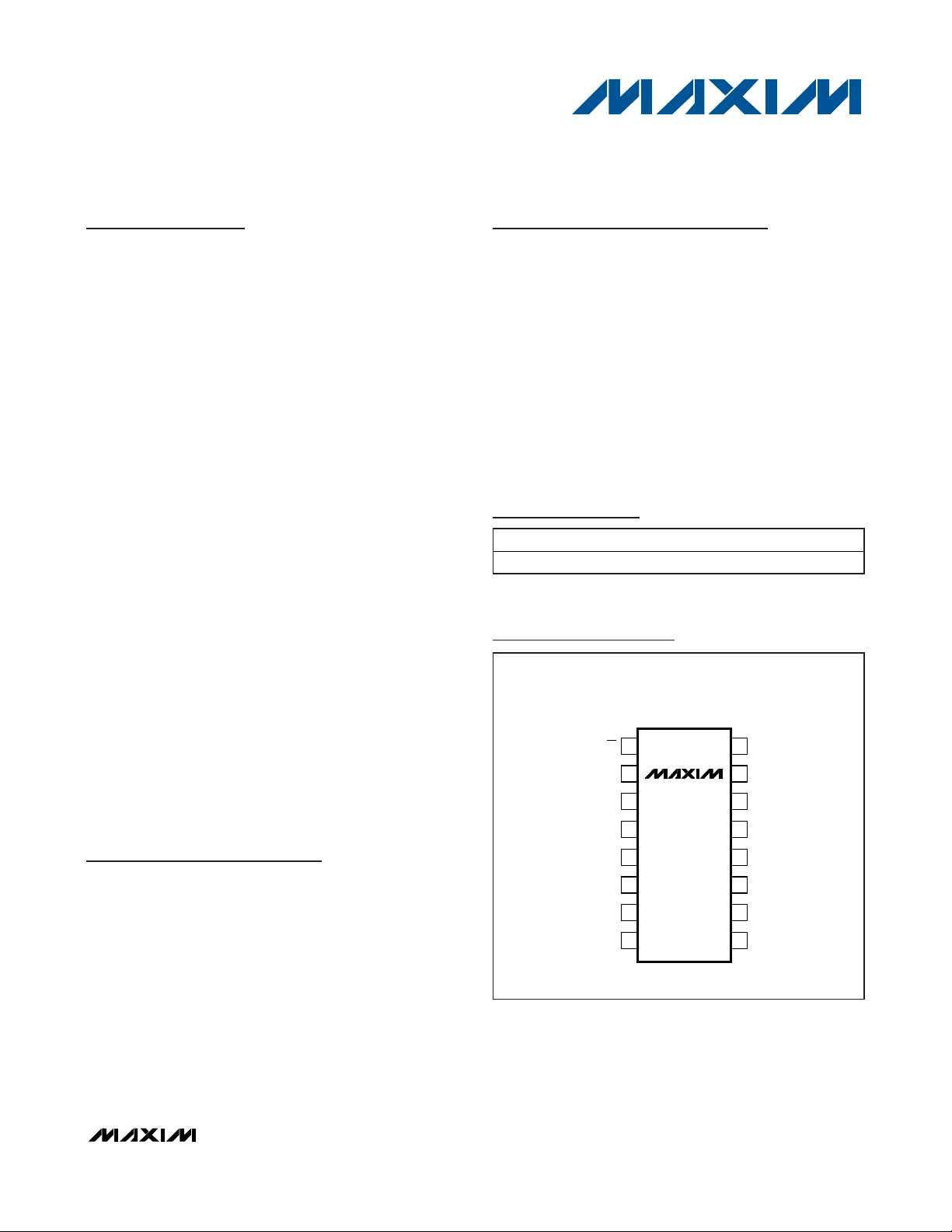
Pin Configuration
Ordering Information
19-4093; Rev 0; 5/08
For pricing, delivery, and ordering information, please contact Maxim Direct at 1-888-629-4642,
or visit Maxim’s website at www.maxim-ic.com.
+
Denotes a lead-free package.
PART TEMP RANGE PIN-PACKAGE
MAX7057ASE+
-40°C to +125°C 16 SO
Typical Application Circuit and Functional Diagram appear
at end of data sheet.
SPI is a trademark of Motorola, Inc.
DGND
DINPAGND
1
+
2
DVDD
GPOSDI
SCLK
CS
TOP VIEW
3
4
AGND
XTAL1
XTAL2
PAVDD
AVDD
5 ENABLEPAOUT
ROUT 6
7
8
MAX7057
14
13
16
15
12
11
10
9
Page 2
MAX7057
300MHz to 450MHz Frequency-Programmable
ASK/FSK Transmitter
2 _______________________________________________________________________________________
ABSOLUTE MAXIMUM RATINGS
DC ELECTRICAL CHARACTERISTICS
(
Typical Application Circuit
, 50Ω system impedance, tuned for 315MHz to 433.92MHz operation, AVDD = DVDD = PAVDD = +2.1V to
+3.6V, f
RF
= 300MHz to 450MHz, f
CRYSTAL
= 16MHz, TA= -40°C to +125°C, unless otherwise noted. Typical values are at AVDD =
DVDD = PAVDD = +2.7V, T
A
= +25°C, unless otherwise noted. All min and max values are 100% tested at TA= +125°C, and guaran-
teed by design and characterization over temperature, unless otherwise noted.)
Stresses beyond those listed under “Absolute Maximum Ratings” may cause permanent damage to the device. These are stress ratings only, and functional
operation of the device at these or any other conditions beyond those indicated in the operational sections of the specifications is not implied. Exposure to
absolute maximum rating conditions for extended periods may affect device reliability.
Supply Voltage, PAVDD, AVDD, DVDD to AGND,
DGND, PAGND ...................................................-0.3V to +4.0V
All Other Pins..................................._GND - 0.3V to _V
DD
+ 0.3V
Continuous Power Dissipation (T
A
= +70°C)
16-Pin SO (derate 8.7mW/°C above +70°C)...............695.7mW
Operating Temperature .....................................-40°C to +125°C
Storage Temperature Range .............................-65°C to +150°C
Lead Temperature (soldering, 10s) .................................+300°C
Supply Voltage V
Supply Current I
DIGITAL I/O
Input High Threshold V
Input Low Threshold V
Input Pulldown Sink Current 13 μA
Input Pullup Source Current 9μA
Output-Voltage High V
Output-Voltage Low V
PARAMETER SYMBOL CONDITIONS MIN TYP MAX UNITS
DD
DD
STDBY
OH
OL
PAVDD, AVDD, and DVDD connected to
power supply, V
PA off, V
duty cycle (ASK)
V
( AS K) ( N otes 1, 2, 3)
V
cycle (FSK) (Note 1)
V
IH
IL
I
I
DIN
at 50% d uty cycl e
D IN
at 100% duty
DIN
< V
ENABLE
= 500μA (GPO)
SINK
= 500μA (GPO) 0.36 V
SOURCE
2.1 2.7 3.6 V
0.9 x
DV
DD
DV
V
-
DD
0.37
at 0%
IL
DD
fRF = 315MHz 3.9 6.5
f
= 433.92MHz 4.5 7.5
RF
fRF = 315MHz 8.1 15.1
= 433.92MHz 8.5 15.0
f
RF
fRF = 315MHz 12.2 23.7
= 433.92MHz 12.4 22.4
f
RF
TA = + 25°C ( N ote 3) 0.8
TA < + 85°C ( N ote 3) 1 6.4Standby Current I
TA < +125°C 6.2 20.1
0.1 x
DD
mA
μA
V
V
V
Page 3
MAX7057
300MHz to 450MHz Frequency-Programmable
ASK/FSK Transmitter
_______________________________________________________________________________________ 3
AC ELECTRICAL CHARACTERISTICS
(
Typical Application Circuit
, 50Ω system impedance, tuned for 315MHz to 433.92MHz operation, AVDD = DVDD = PAVDD = +2.1V to
+3.6V, fRF= 300MHz to 450MHz, f
CRYSTAL
= 16MHz, TA= -40°C to +125°C, unless otherwise noted. Typical values are at AVDD =
DVDD = PAVDD = +2.7V, T
A
= +25°C, unless otherwise noted. All min and max values are 100% tested at TA= +125°C, and guaran-
teed by design and characterization over temperature, unless otherwise noted.)
PARAMETER SYMBOL CONDITIONS MIN TYP MAX UNITS
GENERAL CHARACTERISTICS
Frequency Range 300 450 MHz
Power-On Time t
Maximum Data Rate
Frequency Switching Time
PHASE-LOCKED LOOP (PLL)
VCO Gain K
PLL Phase Noise
Loop Bandwidth 300 kHz
Reference Frequency Input Level 500 mV
Frequency-Divider Range 19 28
Frequency Deviation (FSK) ±2 ±100 kHz
CRYSTAL OSCILLATOR
Crystal Frequency f
Frequency Pulling by V
Crystal Load Capacitance (Note 4) 10 pF
POWER AMPLIFIER (PA)
Output Power (Note 1) P
Modulation Depth 71 dB
Maximum Carrier Harmonics
Reference Spur -45 dBc
DD
ON
VCO
XTAL
OUT
ENABLE transition low-to-high, frequency
settled to within 50kHz of the desired carrier
ENABLE transition low-to-high, frequency
settled to within 5kHz of the desired carrier
ASK mode
FSK mode
Time from end of SPI write to frequency
settled to within 5kHz of desired carrier
fRF = 315MHz
f
= 433.92MHz
RF
TA = +25°C (Note 3) 3.8 9.2 16.4
TA = +125°C, AVDD = DVDD = PAVDD =
+2.1V
TA = -40°C, AVDD = DVDD = PAVDD =
+3.6V (Note 3)
With output matching
network
Manchester encoded 50
Nonreturn-to-Zero 100
Manchester encoded 50
Nonreturn-to-Zero 100
10kHz offset -78
1MHz offset -98
10kHz offset -73
1MHz offset -98
10.71 16 23.68 MHz
2.4 5.2
fRF = 315MHz -29
f
= 433.92MHz -44
RF
120
260
70 μs
320 MHz/V
4 ppm/V
12.6 17.0
dBc/Hz
μs
kbps
P-P
dBm
dBc
Page 4
MAX7057
300MHz to 450MHz Frequency-Programmable
ASK/FSK Transmitter
4 _______________________________________________________________________________________
AC ELECTRICAL CHARACTERISTICS (continued)
(
Typical Application Circuit
, 50Ω system impedance, tuned for 315MHz to 433.92MHz operation, AVDD = DVDD = PAVDD = +2.1V to
+3.6V, fRF= 300MHz to 450MHz, f
CRYSTAL
= 16MHz, TA= -40°C to +125°C, unless otherwise noted. Typical values are at AVDD =
DVDD = PAVDD = +2.7V, T
A
= +25°C, unless otherwise noted. All min and max values are 100% tested at TA= +125°C, and guaran-
teed by design and characterization over temperature, unless otherwise noted.)
Note 1: Supply current and output power are greatly dependent on board layout and PAOUT match.
Note 2: 50% duty cycle at 10kHz ASK data (Manchester coded).
Note 3: Guaranteed by design and characterization, not production tested.
Note 4: Dependent on PCB trace capacitance.
Figure 1. SPI Timing Diagram
PARAMETER SYMBOL CONDITIONS MIN TYP MAX UNITS
SERIAL INTERFACE (SPI) TIMING CHARACTERISTICS (Figure 1)
Minimum SCLK Low to FallingEdge of CS Setup Time
Minimum CS Low to Rising-Edge
of SCLK Setup Time
Minimum SCLK Low to RisingEdge of CS Setup Time
Minimum SCLK Low After RisingEdge of CS Hold Time
Minimum Data Valid to SCLK
Rising-Edge Setup Time
Minimum Data Valid to SCLK
Rising-Edge Hold Time
Minimum SCLK High Pulse Width t
Minimum SCLK Low Pulse Width t
Minimum CS High Pulse Width t
Maximum Transition Time from
Falling-Edge of CS to Valid GPO
Maximum Transition Time from
Falling-Edge of SCLK to Valid
GPO
t
t
CSS
t
HCS
t
t
t
DH
CH
CSH
t
CSG
t
CG
SC
HS
DS
CL
CL = 10pF load capacitance from GPO to
DGND
CL = 10pF load capacitance from GPO to
DGND
10 ns
5ns
20 ns
5ns
10 ns
5ns
40 ns
40 ns
40 ns
50 ns
50 ns
t
t
HCS
CSH
t
HS
SCLK
SDI
GPO
CS
t
SC
t
CSG
t
CSS
t
DS
t
DH
t
CG
t
CH
t
CL
Page 5
MAX7057
300MHz to 450MHz Frequency-Programmable
ASK/FSK Transmitter
_______________________________________________________________________________________ 5
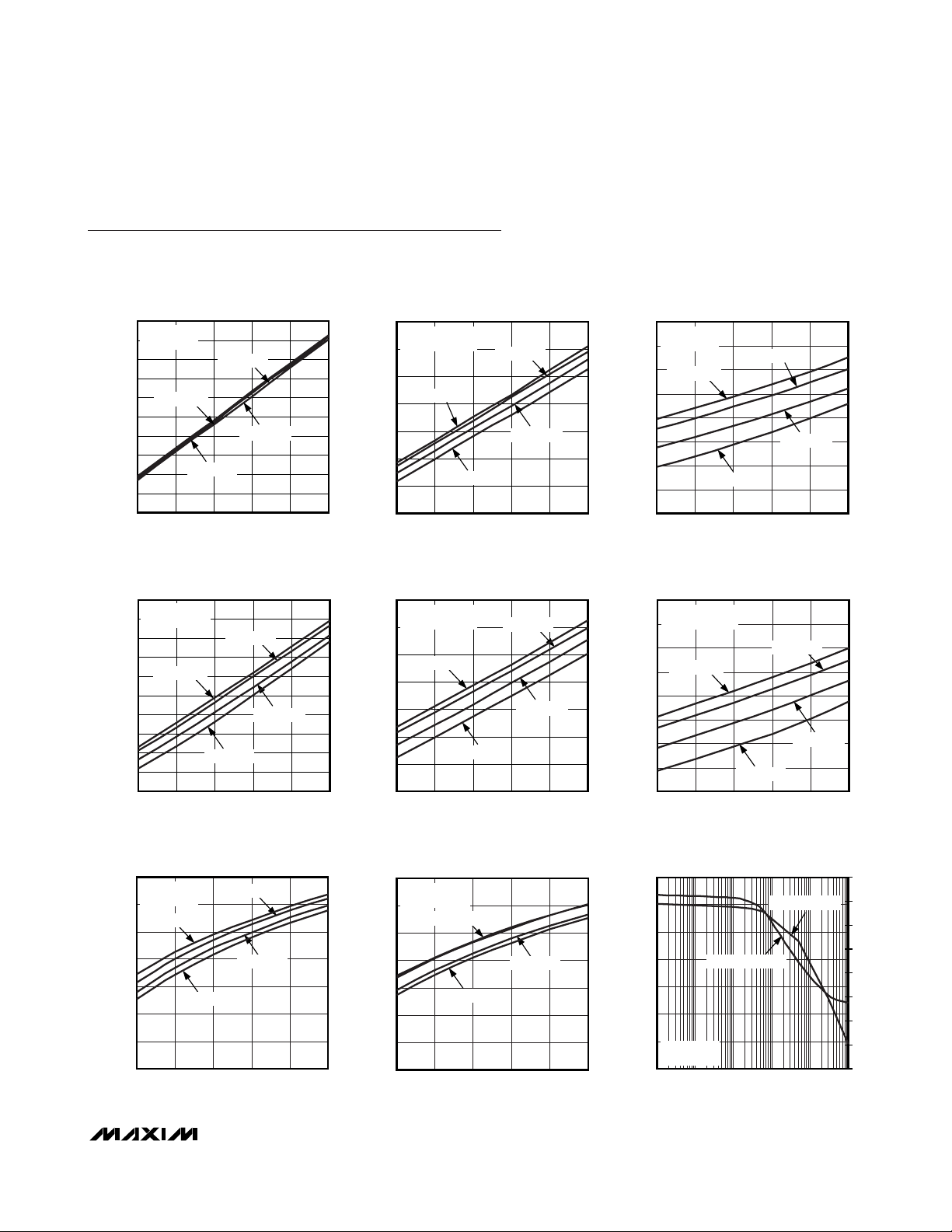
Typical Operating Characteristics
(50Ω system impedance, AVDD = DVDD = PAVDD = +2.1V to +3.6V, fRF= 300MHz to 450MHz, TA= -40°C to +125°C, unless otherwise noted. Typical values are at AVDD = DVDD = PAVDD = +2.7V, T
A
= +25°C, unless otherwise noted.)
OUTPUT POWER
vs. SUPPLY VOLTAGE
MAX7057 toc07
SUPPLY VOLTAGE (V)
OUTPUT POWER (dBm)
3.33.02.72.4
2
4
6
8
10
14
12
0
2.1 3.6
fRF = 315MHz
PA ON
TA = +85°C
TA = +125°C
TA = +25°C
TA = -40°C
OUTPUT POWER
vs. SUPPLY VOLTAGE
MAX7057 toc08
SUPPLY VOLTAGE (V)
OUTPUT POWER (dBm)
3.33.02.72.4
2
4
6
8
10
14
12
0
2.1 3.6
fRF = 433.92MHz
PA ON
TA = +85°C
TA = +125°C
TA = -40°C, +25°C
SUPPLY CURRENT AND OUTPUT POWER
vs. EXTERNAL RESISTOR
MAX7057 toc09
EXTERNAL RESISTOR (Ω)
SUPPLY CURRENT (mA)
OUTPUT POWER (dBm)
1000100101
2
4
6
8
10
14
12
0
-15
-10
-5
0
5
15
10
-25
-20
0.1 10,000
fRF = 315MHz
PA ON
SUPPLY CURRENT
OUTPUT POWER
SUPPLY CURRENT
vs. SUPPLY VOLTAGE
18
fRF = 315MHz
17
PA ON
16
15
14
TA = +125°C
13
12
11
SUPPLY CURRENT (mA)
10
9
8
2.1 3.6
TA = +85°C
TA = +25°C
TA = -40°C
SUPPLY VOLTAGE (V)
SUPPLY CURRENT
vs. SUPPLY VOLTAGE
18
fRF = 433.92MHz
17
PA ON
16
15
TA = +125°C
14
13
12
11
SUPPLY CURRENT (mA)
10
9
8
2.1 3.6
TA = +85°C
TA = +25°C
TA = -40°C
SUPPLY VOLTAGE (V)
12
11
MAX7057 toc01
10
9
8
SUPPLY CURRENT (mA)
7
6
3.33.02.72.4
3.33.02.72.4
5
2.1 3.6
12
11
MAX7057 toc04
10
9
8
SUPPLY CURRENT (mA)
7
6
5
2.1 3.6
SUPPLY CURRENT
vs. SUPPLY VOLTAGE
fRF = 315MHz
50% DUTY CYCLE
TA = +125°C
TA = -40°C
SUPPLY VOLTAGE (V)
SUPPLY CURRENT
vs. SUPPLY VOLTAGE
fRF = 433.92MHz
50% DUTY CYCLE
TA = +125°C
SUPPLY VOLTAGE (V)
TA = +85°C
TA = +25°C
3.33.02.72.4
TA = +85°C
TA = +25°C
TA = -40°C
3.33.02.72.4
MAX7057 toc02
MAX7057 toc05
SUPPLY CURRENT
vs. SUPPLY VOLTAGE
6.0
fRF = 315MHz
PA OFF
5.5
5.0
TA = +125°C
4.5
4.0
3.5
SUPPLY CURRENT (mA)
3.0
2.5
2.0
2.1 3.6
SUPPLY VOLTAGE (V)
TA = +85°C
TA = +25°C
TA = -40°C
SUPPLY CURRENT
vs. SUPPLY VOLTAGE
7.0
fRF = 433.92MHz
PA OFF
6.5
6.0
TA = +125°C
5.5
5.0
4.5
SUPPLY CURRENT (mA)
4.0
3.5
3.0
2.1 3.6
SUPPLY VOLTAGE (V)
TA = +85°C
TA = -40°C
3.33.02.72.4
TA = +25°C
3.33.02.72.4
MAX7057 toc03
MAX7057 toc06
Page 6
MAX7057
300MHz to 450MHz Frequency-Programmable
ASK/FSK Transmitter
6 _______________________________________________________________________________________
Typical Operating Characteristics (continued)
(50Ω system impedance, AVDD = DVDD = PAVDD = +2.1V to +3.6V, fRF= 300MHz to 450MHz, TA= -40°C to +125°C, unless otherwise noted. Typical values are at AVDD = DVDD = PAVDD = +2.7V, T
A
= +25°C, unless otherwise noted.)
SUPPLY CURRENT AND OUTPUT POWER
vs. EXTERNAL RESISTOR
MAX7057 toc10
EXTERNAL RESISTOR (Ω)
SUPPLY CURRENT (mA)
OUTPUT POWER (dBm)
1000100101
2
4
6
8
9
1
3
5
7
0
-15
-10
-5
0
5
10
-25
-20
0.1 10,000
fRF = 315MHz
50% DUTY CYCLE
SUPPLY CURRENT
OUTPUT POWER
SUPPLY CURRENT AND OUTPUT POWER
vs. EXTERNAL RESISTOR
MAX7057 toc11
EXTERNAL RESISTOR (Ω)
SUPPLY CURRENT (mA)
OUTPUT POWER (dBm)
1000100101
2
4
6
8
10
14
12
0
-15
-10
-5
0
5
15
10
-25
-20
0.1 10,000
fRF = 433.92MHz
PA ON
SUPPLY CURRENT
OUTPUT POWER
SUPPLY CURRENT AND OUTPUT POWER
vs. EXTERNAL RESISTOR
MAX7057 toc12
EXTERNAL RESISTOR (Ω)
SUPPLY CURRENT (mA)
OUTPUT POWER (dBm)
1000100101
2
4
6
8
9
1
3
5
7
0
-15
-10
-5
0
5
10
-30
-20
0.1 10,000
fRF = 433.92MHz
50% DUTY CYCLE
SUPPLY CURRENT
OUTPUT POWER
-25
MAX7057 toc13
PHASE NOISE vs. OFFSET FREQUENCY
-60
-70
-80
-90
-100
-110
-120
-130
-140
100 10k 100k 1M 10M1k
OFFSET FREQUENCY (Hz)
PHASE NOISE (dBc/Hz)
fRF = 315MHz
-50
-60
-70
-80
-90
-100
-110
-120
-130
100 10k 100k 1M 10M1k
PHASE NOISE vs. OFFSET FREQUENCY
MAX7057 toc14
OFFSET FREQUENCY (Hz)
PHASE NOISE (dBc/Hz)
fRF = 433.92MHz
-60
-50
-55
-40
-45
-35
-30
2.1 3.6
REFERENCE SPUR MAGNITUDE
vs. SUPPLY VOLTAGE
MAX7057 toc15
SUPPLY VOLTAGE (V)
REFERENCE SPUR MAGNITUDE (dBc)
2.72.4 3.0 3.3
fRF = 433.92MHz
fRF = 315MHz
Page 7

MAX7057
300MHz to 450MHz Frequency-Programmable
ASK/FSK Transmitter
_______________________________________________________________________________________
7
Typical Operating Characteristics (continued)
(50Ω system impedance, AVDD = DVDD = PAVDD = +2.1V to +3.6V, fRF= 300MHz to 450MHz, TA= -40°C to +125°C, unless otherwise noted. Typical values are at AVDD = DVDD = PAVDD = +2.7V, TA= +25°C, unless otherwise noted.)
EFFICIENCY
vs. SUPPLY VOLTAGE
MAX7057 toc18
SUPPLY VOLTAGE (V)
EFFICIENCY (%)
3.33.02.72.4
13
11
17
21
25
9
15
19
23
2.1 3.6
fRF = 315MHz
50% DUTY CYCLE
TA = +85°C
TA = +125°C
TA = +25°C
TA = -40°C
EFFICIENCY
vs. SUPPLY VOLTAGE
MAX7057 toc19
SUPPLY VOLTAGE (V)
EFFICIENCY (%)
3.33.02.72.4
15
20
25
30
35
10
2.1 3.6
fRF = 433.92MHz
PA ON
TA = +85°C
TA = +125°C
TA = +25°C
TA = -40°C
EFFICIENCY
vs. SUPPLY VOLTAGE
MAX7057 toc20
SUPPLY VOLTAGE (V)
EFFICIENCY (%)
3.33.02.72.4
11
13
15
17
19
21
23
9
2.1 3.6
fRF = 433.92MHz
50% DUTY CYCLE
TA = +85°C
TA = +25°C
TA = +125°C
TA = -40°C
-76
-56
-66
-36
-46
-16
-26
-6
+14
+4
+24
FSK SPECTRUM
MAX7057 toc21
(dBm)
100kHz DEVIATION, 4kHz SQUARE-WAVE
MODULATION. SPAN = 1.00MHz
-10
-4
-6
-8
-2
0
2
4
6
8
10
2.1 2.72.4 3.0 3.3 3.6
FREQUENCY STABILITY
vs. SUPPLY VOLTAGE
MAX7057 toc16
SUPPLY VOLTAGE (V)
FREQUENCY STABILITY (ppm)
fRF = 433.92MHz
fRF = 315MHz
EFFICIENCY
vs. SUPPLY VOLTAGE
MAX7057 toc17
SUPPLY VOLTAGE (V)
EFFICIENCY (%)
3.33.02.72.4
15
20
25
30
35
10
2.1 3.6
fRF = 315MHz
PA ON
TA = +85°C
TA = +125°C
TA = +25°C
TA = -40°C
Page 8

MAX7057
300MHz to 450MHz Frequency-Programmable
ASK/FSK Transmitter
8 _______________________________________________________________________________________
Pin Description
Detailed Description
The MAX7057 is frequency programmable from 300MHz
to 450MHz, by using a fractional-N phase-locked loop
(PLL), and transmits data using either ASK or FSK modulation. The MAX7057 has integrated tuning capacitors
at the output of the power amplifier (PA) to ensure highpower efficiency at various programmable frequencies
with a single-matching network.
The crystal-based architecture of the MAX7057 eliminates many of the common problems with SAW transmitters by providing greater modulation depth, faster
frequency settling, tighter transmit frequency tolerance,
and reduced temperature dependence. In particular,
the tighter transmit frequency tolerance means that a
superheterodyne receiver with a narrower IF bandwidth
(therefore lower noise bandwidth) can be used. The
payoff is better overall receiver performance when using
a superheterodyne receiver such as the MAX1471,
MAX1473, MAX7033, MAX7034, or MAX7042.
Frequency Programming
The MAX7057 is a crystal-referenced phased-locked
loop (PLL) VHF/UHF transmitter that transmits data over
the frequency range of 300MHz to 450MHz in ASK or
FSK mode. The transmit frequency is set by the crystal
frequency and the programmable divider in the PLL;
the programmable-divide ratios can be set anywhere
from 19 to 28, which means that with a crystal frequency of 16MHz, the output frequency range can be from
304MHz to 448MHz.
The fractional-N architecture of the PLL in the MAX7057
allows the FSK signal to be programmed for exact frequency deviations and rapid, transient-free frequency
settling time. This modulation method completely elimi-
PIN NAME FUNCTION
1 CS Serial Interface Active-Low Chip Select. Internally pulled up to DVDD.
2 SDI Serial Interface Data Input. Internally pulled down to GND.
3 SCLK Serial Interface Clock Input. Internally pulled down to GND.
4 PAGND Power Amplifier Ground
5 PAOUT
6ROUT
Power Amplifier Output. Requires a pullup inductor to the supply voltage or ROUT. The pullup inductor can
be part of the output-matching network.
Envelope-Shaping Output. ROUT controls the power amplifier envelope’s rise and fall times. Connect
ROUT to the PA pullup inductor or to an optional power-adjust resistor. Bypass the inductor to GND as
close as possible to the inductor with 680pF and 220pF capacitors.
7 PAVDD
8 AVDD
9 XTAL2 Crystal Input 2. XTAL2 can be driven from an AC-coupled external reference.
10 XTAL1 Crystal Input 1. Bypass to ground if XTAL2 is driven from an AC-coupled external reference.
11 AGND Analog Ground
12 ENABLE
13 DIN
14 DGND Digital Ground
15 GPO
16 DVDD
Power Amplifier Supply Voltage. Bypass to ground with 0.01μF and 220pF capacitors placed as close as
possible to the pin.
Analog Positive Supply Voltage. Bypass to ground with 0.1μF and 0.01μF capacitors placed as close as
possible to the pin.
Enable Pin. Drive high for normal operation; drive low or leave unconnected to put the device in standby
mode. Internally pulled down to GND.
ASK/FSK Data Input. Use the control register (address: 0x00) to select the type of modulation. Internally
pulled down to GND.
General-Purpose Output. Can be configured to output various digital signals (SPI serial data output—SDO,
CLKOUT—reference oscillator frequency divided by 1, 2, 4, or 8 for microprocessor clock, etc).
Digital positive supply voltage. Bypass to ground with 0.1μF and 0.01μF capacitors placed as close as
possible to the pin.
Page 9

nates the problems associated with crystal-pulling FSK
signal generation. The multiplying factor of the PLL is
set by a 16-bit number, with 4 bits for integer and 12
bits for fraction. The 12-bit fraction in the synthesizer
results in a tuning resolution that is equal to the reference frequency divided by 4096.
The MAX7057 has an internal variable shunt capacitor
connected at the PA output. This capacitor is controlled
using the SPI to maintain highly efficient transmission at
any frequency within a 1.47 to 1 (28/19) tuning range.
This means that it is possible to change the frequency
and retune the antenna to the new frequency in a very
short time. The combination of rapid-antenna tuning
ability with rapid-synthesizer tuning makes the
MAX7057 a true frequency-agile transmitter. The tuning
capacitor has a resolution of 0.25pF. The MAX7057
also features adjustable output power through an external resistor to nearly +10dBm into a 50Ω load at +2.7V.
The MAX7057 supports data rates up to 100kbps NRZ
in both ASK and FSK modes. In FSK mode, the frequency deviation can be programmed as low as ±2kHz
and as high as ±100kHz.
Power Amplifier (PA)
The PA of the MAX7057 is a high-efficiency, open-drain
switching-mode amplifier. In a switching-mode amplifier, the gate of the final-stage FET is driven with a very
sharp 25% duty-cycle square wave at the transmit frequency. This square wave is derived from the synthesizer circuit. When the matching network is tuned
correctly, the output FET resonates the attached matching circuit with a minimum amount of power dissipated
in the FET. With a proper output-matching network, the
PA can drive a wide range of antenna impedances,
which include a small-loop PCB trace and a 50Ω antenna. The output-matching network suppresses the carrier harmonics and transforms the antenna impedance to
an optimal impedance at PAOUT, which is from 125Ω
to 250Ω.
When the output-matching network is properly tuned,
the PA transmits power with a high overall efficiency of
up to 25%. The efficiency of the PA itself is more than
39%. The output power can be adjusted by changing
the impedance seen by the PA or by adjusting the
value of an external resistor at PAOUT.
Envelope Shaping
The MAX7057 features an internal envelope-shaping
resistor for ASK modulation, which connects between
PAVDD and ROUT. When connected to the PA pullup
inductor, the envelope-shaping resistor slows the turnon/-off time of the PA and results in a smaller spectral
width of the modulated PA output signal.
Variable Capacitor
The MAX7057 has a set of internal variable shunt
capacitors that can be switched in and out to present
different capacitor values at the PA output. The capacitors are connected from the PA output to ground. This
allows changing the tuning network along with the synthesizer divide ratio each time the transmitted frequency
changes, making it possible to maintain maximum transmitter power while moving rapidly from one frequency to
another.
When the particular capacitance control bit is high, the
corresponding amount of shunt capacitance is added at
PAOUT. The 32 capacitor values are selected using the
SPI; the capacitance resolution is 0.25pF. The total
capacitance can vary from 0 to 7.75pF. For example, if
cap[1] and cap[3] are high, and cap[4], cap[2], and
cap[0] are low, this circuit will add 2.5pF at PAOUT. See
Table 1 for variable capacitor values and control bits.
Fractional-N Phase-Locked Loop (PLL)
The MAX7057 utilizes a fully integrated fractional-N PLL
for its transmit frequency synthesizer. All PLL components, including the loop filter, are included on-chip.
The loop bandwidth is programmable to either 300kHz
or 600kHz. See Tables 2, 3, and 4 for “pllbw” bit
description. The 16-bit fractional-N topology allows the
transmit frequency to be adjusted in increments of
f
XTAL
/4096. The allowable range of the fRF/f
XTAL
ratio is
approximately 19 to 28.
The fractional-N topology also allows exact FSK frequency deviations to be programmed, completely eliminating the problems associated with generating
frequency deviations by crystal oscillator pulling.
The integer and fractional portions of the PLL divider
ratio set the transmit frequency. The following example
shows how to determine the correct values to be
loaded to registers HIFREQ1, HIFREQ0, LOFREQ1, and
LOFREQ0. See Tables 2, 3, and 7–10 for a detailed
description of these registers.
MAX7057
300MHz to 450MHz Frequency-Programmable
ASK/FSK Transmitter
_______________________________________________________________________________________ 9
Table 1. Variable Capacitor Values and
Control Bits
SPI REGISTER BITS
cap[0] 0.25
cap[1] 0.5
cap[2] 1.0
cap[3] 2.0
cap[4] 4.0
INCREMENTAL SHUNT
CAPACITANCE (pF)
Page 10

MAX7057
Due to the nature of the transmit PLL frequency divider,
a fixed offset of 16 must be subtracted from the transmit PLL divider ratio for programming the MAX7057’s
transmit frequency registers. To determine the value to
program the MAX7057’s transmit frequency registers,
convert the decimal value of the following equation to
the nearest hexadecimal value:
Assume that the ASK transmit frequency = 315MHz
and f
XTAL
= 16MHz. In this example, the rounded decimal value is 15,104, or 0x3B00 hexadecimal. The upper
2 bytes (0x3B) are loaded into the LOFREQ1 register,
and the low 2 bytes (0x00) are loaded into the
LOFREQ0 register. In ASK mode, the transmit frequency equals the lower frequency programmed into the
MAX7057’s transmit frequency registers (see Tables 2,
3, and 9–12).
In FSK mode, the transmit frequencies equal the upper
(HIFREQ1 and HIFREQ0) and lower (LOFREQ1 and
LOFREQ0) frequencies programmed into the MAX7057’s
transmit frequency registers. Calculate the upper and
lower frequency in the same way as shown above. FSK
deviations as low as ±2kHz and as high as ±100kHz are
programmable (see Tables 2, 3, and 8–12).
The exact min and max values for the transmit frequency registers (HIFREQ1/0, LOFREQ1/0) are 2.9596
(0x2F42) and 12.0220 (0xC05A), yielding a synthesizer
ratio of 18.9596 and 28.0220, respectively. These limits
MUST be followed to prevent the delta-sigma modulator from overflowing.
Whenever all of the fractional bits in the HIFREQ1/0 and
LOFREQ1/0 registers are zero (fhi[11:0] and flo[11:0]),
only an integer divider is used, and the delta-sigma
modulator is not in operation. This allows lower current
operation. The 600kHz PLL bandwidth should be used
in this mode to reduce phase noise.
Any change to the transmit frequency registers must be
followed by writing a “1” to the self-reset frequency load
register (see Tables 2, 3, and 12).
Crystal (XTAL) Oscillator
The crystal (XTAL) oscillator in the MAX7057 is
designed to present a capacitance of approximately
6pF between XTAL1 and XTAL2. In most cases, this
corresponds to an 8pF load capacitance applied to the
external crystal when typical PCB parasitics are added.
The MAX7057 is designed to operate with a typical
10pF load capacitance crystal. It is very important to
use a crystal with a load capacitance that is equal to
the capacitance of the MAX7057 crystal oscillator
plus PCB parasitics and optional external load
capacitors. If a crystal designed to oscillate with a dif-
ferent load capacitance is used, the crystal is pulled
away from its stated operating frequency, introducing
an error in the reference frequency. A crystal designed
to operate at a higher load capacitance than the value
specified for the oscillator is always pulled higher in frequency. Adding capacitance to increase the load
capacitance on the crystal increases the start-up time
and can prevent oscillation altogether.
In actuality, the oscillator pulls every crystal. The crystal’s natural frequency is below its specified frequency,
but when loaded with the specified load capacitance,
the crystal is pulled and oscillates at its specified frequency. This pulling is already accounted for in the
specification of the load capacitance.
Additional pulling can be calculated if the electrical
parameters of the crystal are known. The frequency
pulling is given by:
where:
fp is the amount the crystal frequency is pulled in ppm
C
m
is the motional capacitance of the crystal
C
case
is the case capacitance
C
spec
is the specified load capacitance
C
load
is the actual load capacitance
When the crystal is loaded as specified (i.e., C
load
=
C
spec
), the frequency pulling equals zero.
Communication Protocol
The MAX7057 registers are programmed through an SPI
interface. Figure 2 shows the timing diagram of the SPI.
The GPO must be properly configured to act as an SPI
data output (SDO) by setting the configuration 1 register
(see Tables 2, 3, 15, and 16).
The SPI operates on a byte format, according to Figure 2.
300MHz to 450MHz Frequency-Programmable
ASK/FSK Transmitter
10 ______________________________________________________________________________________
⎛
f
RF
⎜
f
⎝
XTAL
⎞
-16
×=
4096
⎟
⎠
Decimal value to program
transmit frequency registers
⎛
C
m
f
=
p
⎜
2
⎝
11
CCCC
++
case load case spec
⎞
6
×−
10
⎟
⎠
Page 11

Depending on the command, byte 1 through byte N
may assume different functions. They may either be a
direct command (write, read, read all, reset), or an
address or data contents. The commands available in
the MAX7057 SPI are described in detail below:
Write: The write command (0x01) is used to program
the MAX7057 registers (see Tables 2 and 3). The format shown in Figure 3 must be followed, allowing all the
registers to be programmed within one CS cycle.
Using a byte descriptive notation, the write command
can be viewed as the following sequence:
Data 0 is then written to the register addressed by
<Initial Address>, Data 1 is written to <Initial Address +
1>, and so on.
Read: To execute an SPI read operation, the generalpurpose output (GPO) pin must be configured to either
a CKOUT_SDO or SDO function (see Tables 15 and 16
for details).
MAX7057
300MHz to 450MHz Frequency-Programmable
ASK/FSK Transmitter
______________________________________________________________________________________ 11
Figure 2. SPI Format
Figure 3. SPI Write Command Format
CS
SCLK
SDI
CS
SCLK
SDI
D7 D6 D5 D4 D3 D2 D1 D0 D7 D6 D5 D4 D3 D2 D1 D0
DATA 1 DATA N
WRITE COMMAND (0x01) INITIAL ADDRESS (A[7:0]) DATA 0 DATA N
D7 D7D6 D5 D4 D3 D2 D1 D0A7 A6 A5 A4 A3 A2 A1 A0 D0
SDI: <0x01> <Initial Address> <Data 0> <Data 1> … <Data N>
Page 12

MAX7057
300MHz to 450MHz Frequency-Programmable
ASK/FSK Transmitter
12 ______________________________________________________________________________________
Using a byte descriptive notation, the read command
can be viewed as the following sequence, within the
same CS cycle:
With this command, all the registers can be read within
the same cycle of CS. The addresses can be given in
any order.
Read-All: To execute an SPI read-all operation, GPO
must be configured to either a CKOUT_SDO or SDO
function (see Tables 15 and 17 for details).
Using a byte descriptive notation, the read command
can be viewed as the following sequence, within two
CS cycles:
Reset: The MAX7057 can be reset to its power-up state
through the reset command.
Figure 4. SPI Read Command Format
Figure 5. SPI Read-All Command Format
CS
SCLK
SDI
GPO
CS
SCLK
SDI
READ COMMAND (0x02) ADDRESS 0 ADDRESS 1 0x00
READ ALL COMMAND (0x03) ADDRESS N
A7 A6 A5 A4 A3 A2 A1 A0 A7 A7
A7 A6 A5 A4 A3 A2 A1 A0
A6 A5 A4 A3 A2 A1 A0 A0
D7 D6 D5 D4 D3 D2 D1 D0
DATA 0 DATA N
D7 D7 D7D6 D5 D4 D3 D2 D1 D0 D0 D0GPO
DATA N
ADDRESS
D7
DATA
N - 1
DATA
N + 1
N
D7
D0 D0
DATA
N + n
SDI : <0x02> <Address 0> <Address 1> <Address2> … <
GPO: < XX > < XX > < Data 0 > < Data 1 > … < Data N - 1 > <Data N>
Address N > < 0x00 >
SDI : <0x03> <Address N> < XX > < XX > < XX >…< XX >
GPO:
CS cycle 1
<Data N> <DataN + 1> <DataN + 2>…<Data N + n>
CS cycle 2
Page 13

Using a byte descriptive notation, the reset command
can be viewed as the following sequence, within the
same CS cycle:
SDI: <0x04>
Features and Settings
Values and parameters are set through registers in the
MAX7057 that are addressable through the SPI. These
registers contain bits that either turn functions on and
off or program numerical settings. The following settings are controlled through the SPI.
Variable Capacitor
The internal variable shunt capacitor, which is instrumental in matching the PA to the antenna, is controlled
by setting 5 bits in the configuration 0 register. This
allows for 32 levels of shunt capacitance control. Since
the control of these 5 bits is independent of the other
settings, any capacitance value can be chosen at any
frequency, making it possible to maintain maximum
transmitter efficiency while moving rapidly from one frequency to another.
Clock Output
The MAX7057 has a buffered clock output that can
serve as a clock for a microprocessor. The divide ratio
is set through the configuration 0 register (see Tables 5
and 6). The divide settings are 1 (no division), 2, 4, 8, or
16; the original undivided frequency is based on the
reference frequency generated by the external crystal.
The buffered clock output is available at GPO when
enabled by setting the configuration 1 register (see
Tables 2, 3, 15, and 16).
Mode Select and Crystal Shutdown
The transmission mode is selected by writing to a register. The default mode is ASK and the mode can be
changed to FSK by writing a 1 to the mode bit in the
control register. This register is also used to keep the
crystal circuit powered up in the shutdown mode.
Registers
The following tables provide information on the
MAX7057 registers.
MAX7057
300MHz to 450MHz Frequency-Programmable
ASK/FSK Transmitter
______________________________________________________________________________________ 13
Figure 6. Reset Command Format
Table 2. Register Summary
CS
SCLK
SDI
RESET COMMAND (0x04)
ADDRESS REGISTER NAME DESCRIPTION
0x00 CONTRL
0x01 CONFIG0
0x02 HIFREQ1 High-frequency 1 register (upper byte). Sets the high frequency in FSK transmission.
0x03 HIFREQ0 High-frequency 0 register (lower byte). Sets the high frequency in FSK transmission.
0x04 LOFREQ1
0x05 LOFREQ0
0x06 FLOAD Frequency load register. Performs the frequency load function.
0x07 DATAIN Data in register. SPI equivalent of DIN pin.
0x08 EN Enable register. SPI equivalent of ENABLE pin.
0x09 CONFIG1 Configuration 1 register. GPO selector.
0x0C STATUS Status register.
Control register. Controls the mode (ASK/FSK), crystal clock output, envelope-shaping, PLL
bandwidth, and SPI enable.
Configuration 0 register. Controls the capacitance at the PA output and clock output
frequency divider.
Low-frequency 1 register (upper byte). Sets the low frequency in FSK transmission, or
carrier frequency in ASK transmission.
Low-frequency 0 register (lower byte). Sets the low frequency in FSK transmission, or carrier
frequency in ASK transmission.
Page 14

MAX7057
300MHz to 450MHz Frequency-Programmable
ASK/FSK Transmitter
14 ______________________________________________________________________________________
Table 5. Configuration 0 Register (Address: 0x01)
Table 3. Register Configuration
Table 4. Control Register (Address: 0x00)
NAME ADDRESS
CONTRL 0x00 0 0 spioffsht pllbw shape ckouts ckouton mode R/W
CONFIG0 0x01 ckdiv[2] ckdiv[1] ckdiv[0] cap[4] cap[3] cap[2] cap[1] cap[0] R/W
HIFREQ1 0x02 fhi[15] fhi[14] fhi[13] fhi[12] fhi[11] fhi[10] fhi[9] fhi[8] R/W
HIFREQ0 0x03 fhi[7] fhi[6] fhi[5] fhi[4] fhi[3] fhi[2] fhi[1] fhi[0] R/W
LOFREQ1 0x04 flo[15] flo[14] flo[13] flo[12] flo[11] flo[10] flo[9] flo[8] R/W
LOFREQ0 0x05 flo[7] flo[6] flo[5] flo[4] flo[3] flo[2] flo[1] flo[0] R/W
FLOAD 0x06 — — — — — — — fload R/W
DATAIN 0x07 — — — — — — — datain_bit R/W
EN 0x08 — — — — — — — enable_bit R/W
CONFIG1 0x09 0 0 0 0 0 gposel[2] gposel[1] gposel[0] R/W
STATUS 0x0C fhi/lo[15] fhi/lo[14] fhi/lo[13] fhi/lo[12] X 0 TxREADY NoXTAL R
BIT 7 BIT 6 BIT 5 BIT 4 BIT 3 BIT 2 BIT 1 BIT 0 MODE
DATA
BIT NAME FUNCTION
0 mode ASK(0) or FSK(1)
1 ckouton Crystal clock output enable(1) on GPO output
2 ckouts Crystal clock output enable(1) while part is in shutdown mode
3 shape Disable(0) or enable(1) transmitter envelope-shaping resistor
4 pllbw
5 spioffsht Enable(0) or disable(1) SPI communication during shutdown
PLL bandwidth setting, low(0) = 300kHz or high(1) = 600kHz; 300kHz is recommended for fractional-N
and 600kHz for fixed-N
BIT NAME FUNCTION
4-0 cap[4:0] 5-bit capacitor setting
7-5 ckdiv[2:0] 3-bit clock output frequency divider
Page 15

The 4 MSBs of HIFREQ1 (fhi[15:12]) are the integer
portion of the divider, excluding offset of 16. The 12
LSBs (fhi[11:0]) are the fractional part of the divider.
MAX7057
300MHz to 450MHz Frequency-Programmable
ASK/FSK Transmitter
______________________________________________________________________________________ 15
Table 6. ckdiv[2:0] of Configuration 0 Register (Address: 0x01)
Table 7. High-Frequency 1 Register (Address: 0x02)
Table 8. High-Frequency 0 Register (Address: 0x03)
Table 9. Low-Frequency 1 Register (Address: 0x04)
Table 10. Low-Frequency 0 Register (Address: 0x05)
Table 11. Maximum and Minimum Values for Frequency Divide
The 4 MSBs of LOFREQ1 (flo[15:12]) are the integer
portion of the divider, excluding offset of 16. The 12
LSBs (flo[11:0]) are the fractional part of the divider.
Valid values for the divider are shown in Table 11.
DECIMAL BINARY CRYSTAL FREQUENCY DIVIDED BY
0 000 1
1 001 2
2 010 4
3 011 8
4-7 1XX 16
BIT NAME FUNCTION
7-0 fhi[15:8] 8-bit upper byte of high-frequency divider for FSK
BIT NAME FUNCTION
7-0 fhi[7:0] 8-bit lower byte of high-frequency divider for FSK
BIT NAME FUNCTION
7-0 flo[15:8] 8-bit upper byte of low-frequency divider for FSK/ASK
BIT NAME FUNCTION
7-0 flo[7:0] 8-bit lower byte of low-frequency divider for FSK/ASK
DECIMAL VALUE fhi[15:12], flo[15:12] fhi[11:0], flo[11:0]
12.0220 0xC 0x05A
2.9536 0x2 0xF42
Page 16

MAX7057
These values are internally summed with 16, and thus,
the min and max divider becomes approximately 19
and 28. These limits MUST be followed, to prevent the
delta-sigma number generator from overflowing.
Whenever all of the fhi[11:0] and flo[11:0] are zero, only
an integer divider is used, and the delta-sigma modulator is not in operation. This allows lower current operation. The 600kHz PLL bandwidth could be used in this
mode to reduce phase noise.
300MHz to 450MHz Frequency-Programmable
ASK/FSK Transmitter
16 ______________________________________________________________________________________
Table 12. Frequency Load Register (Address: 0x06)
Table 13. Data In Register (Address: 0x07)
Table 14. Enable Register (Address: 0x08)
Table 15. Configuration 1 Register (Address: 0x09)
Table 16. General-Purpose Output Selector (gposel[2:0]) for Configuration 1 Register
BIT NAME FUNCTION
0 fload
Effectively changes the PLL frequency to the ones written in registers 2–5. This is a self-reset bit,
and is reset to zero after the operation is completed.
BIT NAME FUNCTION
SPI equivalent of DIN, where the transmitted data can be controlled through the SPI interface. It
0 datain_bit
should be kept low (0) if only the external DIN pin is used. The external DIN pin should also be kept
low (0) if the SPI datain_bit is used.
BIT NAME FUNCTION
0 enable_bit
SPI equivalent of ENABLE. It should be kept low (0) if the external ENABLE pin is used. The external
ENABLE pin should also be kept low (0) if the SPI enable_bit is used.
BIT NAME FUNCTION
2-0 gposel[2:0] 3-bit GPO selector
7-3 RESERVED “0” RESERVED. Set to 0 for normal operation.
DECIMAL BINARY GPO DESCRIPTION
0 000 CKOUT_SDO
1 001 SDO SPI Serial Data Output (SDO)
2 010 CKOUT Clock Output
3 011 RESERVED RESERVED
4 100 RESERVED RESERVED
5 101 NoXTAL Internal Crystal Oscillator Status. High means oscillator is NOT in operation.
6 110 TxREADY
7 111 datain_bit A copy of datain_bit
Clock/SDO Output. Outputs clock when CS is high and clock output is enabled;
outputs SDO when CS is low.
Transmitter Ready Status. High means PLL is locked and MAX7057 is ready to
transmit data.
Page 17

Applications Information
Output Matching to 50
Ω
When matched to a 50Ω system, the MAX7057’s PA is
capable of delivering +9.2dBm of output power at
PAVDD = +2.7V with a broadband match. The output of
the PA is an open-drain transistor, which has internal
selectable shunt tuning capacitors (see the
Variable
Capacitor
section) for impedance matching. It is connected to PAVDD or ROUT through a pullup inductor
for proper biasing. The internal selectable shunt capacitors make it easy for tuning when changing the output
frequency. The pullup inductor from the PA to PAVDD
or ROUT serves three main purposes: resonating the
capacitive PA output, providing biasing for the PA, and
acting as a high-frequency choke to prevent RF energy
from coupling onto the supply voltage. The pi network
between the PA output and the antenna also forms a
lowpass filter that provides attenuation for the higherorder harmonics.
Output Matching to PCB Loop Antenna
In many applications, the MAX7057 must be impedance-matched to a small-loop antenna. The antenna is
usually fabricated out of a copper trace on a PCB in a
rectangular, circular, or square pattern. The antenna
has an impedance that consists of a lossy component
and a radiative component. To achieve high radiating
efficiency, the radiative component should be as high
as possible, while minimizing the lossy component. In
addition, a loop antenna has an inherent loop inductance associated with it (assuming the antenna is terminated to ground). In a typical application, the
inductance of the loop antenna is approximately 50nH
to 100nH. The radiative and lossy impedances can be
anywhere from a few tenths of an ohm to 5Ω or 10Ω.
Layout Considerations
A properly designed PCB is an essential part of any
RF/microwave circuit. At high-frequency inputs and outputs, use controlled-impedance lines and keep them as
short as possible to minimize losses and radiation. At
high frequencies, trace lengths that are in the order of
λ/10 or longer act as antennas, where λ is the wavelength.
Keeping the traces short also reduces parasitic inductance. Generally, 1in of PCB trace adds about 20nH of
parasitic inductance. The parasitic inductance can
have a dramatic effect on the effective inductance of a
passive component. For example, a 0.5in trace connecting to a 100nH inductor adds an extra 10nH of
inductance, or 10%.
To reduce parasitic inductance, use wider traces and a
solid ground or power plane below the signal traces.
Using a solid ground plane can reduce the parasitic
inductance from approximately 20nH/in to 7nH/in. Also,
use low-inductance connections to the ground plane,
and place decoupling capacitors as close as possible
to all VDDpins.
MAX7057
300MHz to 450MHz Frequency-Programmable
ASK/FSK Transmitter
______________________________________________________________________________________ 17
Table 17. Status Register (Address: 0x0C)
BIT NAME FUNCTION
0 NoXTAL Internal Crystal Oscillator Status. High means oscillator is not in operation.
1 TxREADY Transmitter Ready Status. High means PLL is locked and MAX7057 is ready to transmit data.
2 RESERVED “0” RESERVED. Set to 0 for normal operation.
3 X RESERVED
7-4 fhi/lo[15]–fhi/lo[12]
ASK mode: Outputs flo[15:12].
FS K m od e: w hen d atai n p i n/b i t i s hi g h, outp uts fhi [ 15:12] ; w hen d atai n p i n/b i t i s l ow , outp uts fl o[ 15:12] .
Page 18

MAX7057
300MHz to 450MHz Frequency-Programmable
ASK/FSK Transmitter
18 ______________________________________________________________________________________
Typical Application Circuit
Component List
SCLK
SDI
V
DD
GPO
DIN
ENABLE
CS
12
CS
XTAL1
9
10
C11
DVDD
GPO
DGND
ENABLE
AGND
DIN
16
C12 C13
15
14
13
12
11
SCLK
PAGND
PAOUT
ROUT
PAVDD
SDI
MAX7057
AVDD
V
DD
XTAL2
8
C10
3
4
C1
RF
L1
OUT
C3
C2
L2
C4C5
5
R1
6
V
DD
7
C6C7
C9 C8
C15 C14
Y1
DESIGNATION QTY DESCRIPTION
C1, C2 1
C3 1
C4, C7 2
C5 1
C6, C9, C12 3
C8, C13 2
C10, C11 2
C14, C15 2
L1 1
L2 1
10pF ±5%, 50V C0G ceramic capacitor (0603)
Murata GRM1885C1H100J
6.8pF ±5%, 50V C0G ceramic capacitor (0603)
Murata GRM1885C1H6R8J
220pF ±5%, 50V C0G ceramic capacitors (0603)
Murata GRM1885C1H221J
680pF ±5%, 50V C0G ceramic capacitor (0603)
Murata GRM1885C1H681J
10nF ±10%, 50V X7R ceramic capacitors (0603)
Murata GRM188R71H103K
100nF ±10%, 50V X7R ceramic capacitors (0603)
Murata GRM188R71H104K
100pF ±5%, 50V C0G ceramic capacitors (0603)
Murata GRM1885C1H101J
4pF ±5%, 50V C0G ceramic capacitors (0603)
Murata GRM1885C1H4R0C
22nH ±5% wire-wound inductor (0603)
Murata LQW18AN22NJ00
13nH ±5% wire-wound inductor (0603)
Murata LQW18AN13NJ00
R1 1 0Ω resistor (0603)
Y1 1 16MHz crystal, Crystek 17466, Suntsu SCX284
Page 19

MAX7057
300MHz to 450MHz Frequency-Programmable
ASK/FSK Transmitter
Maxim cannot assume responsibility for use of any circuitry other than circuitry entirely embodied in a Maxim product. No circuit patent licenses are
implied. Maxim reserves the right to change the circuitry and specifications without notice at any time.
Maxim Integrated Products, 120 San Gabriel Drive, Sunnyvale, CA 94086 408-737-7600 ____________________
19
© 2008 Maxim Integrated Products is a registered trademark of Maxim Integrated Products, Inc.
Functional Diagram
Chip Information
PROCESS: CMOS
PACKAGE TYPE PACKAGE CODE DOCUMENT NO.
16 SO S16+3
21-0041
Package Information
For the latest package outline information, go to
www.maxim-ic.com/packages
.
PAOUT
ROUT
SDI
SCLK
3
MAX7057
SERIAL INTERFACE AND
DIGITAL CONTROL
4PAGND
5
6
PA
ENVELOPE
SHAPING
PAVDD
DELTA-SIGMA
MODULATOR
LOOP
FILTER
7
CS
DVDD
1
2
FREQUENCY
DIVIDER
PFDVCO
CHARGE
PUMP
AVDD XTAL1
16
8
XTAL2
CRYSTAL
OSCILLATOR
9 10
14 DGND
13 DIN
12 ENABLE
15 GPO
11
AGND
 Loading...