

Page 1
General Description
The MAX7042 fully integrated, low-power, CMOS
superheterodyne RF receiver is designed to receive
frequency-shift-keyed (FSK) data at rates up to 66kbps
nonreturn-to-zero (NRZ) (33kbps Manchester). The
MAX7042 requires only a few external components to
realize a complete wireless RF receiver at 308, 315,
418, and 433.92MHz.
The MAX7042 includes all the active components
required in a superheterodyne receiver including a lownoise amplifier (LNA), an image-rejection (IR) mixer, a
fully integrated phase-locked loop (PLL), local oscillator
(LO), 10.7MHz IF limiting amplifier with received-signalstrength indicator (RSSI), low-noise FM demodulator,
and a 3V regulator. Differential peak-detecting data
demodulators are included for baseband data recovery.
The MAX7042 is available in a 32-pin thin QFN and
is specified over the automotive -40°C to +125°C
temperature range.
Applications
Remote Keyless Entry
Tire-Pressure Monitoring
Home and Office Lighting Control
Remote Sensing
Smoke Alarms
Home Automation
Local Telemetry Systems
Security Systems
Features
♦ +2.4V to +3.6V or +4.5V to +5.5V Single-Supply
Operation
♦ Four User-Selectable Carrier Frequencies
308, 315, 418, and 433.92MHz
♦ -110dBm RF Input Sensitivity at 315MHz
♦ -109dBm RF Input Sensitivity at 433.92MHz
♦ Fast Startup (<250µs)
♦ Small 32-Pin Thin QFN Package
♦ Low Operating Supply Current
6.2mA Continuous
20nA Power-Down
♦ Integrated PLL, VCO, and Loop Filter
♦ 45dB Integrated Image Rejection
♦ Selectable IF BW with External Filter
♦ Positive and Negative Peak Detectors
♦ RSSI Output
MAX7042
308MHz/315MHz/418MHz/433.92MHz
Low-Power, FSK Superheterodyne Receiver
________________________________________________________________ Maxim Integrated Products 1
Pin Configuration
Ordering Information
19-3704; Rev 0; 5/05
For pricing, delivery, and ordering information, please contact Maxim/Dallas Direct! at
1-888-629-4642, or visit Maxim’s website at www.maxim-ic.com.
*EP = Exposed pad.
Typical Application Circuit appears at end of data sheet.
PART
MAX7042ATJ
TEMP
RANGE
-40°C to
+125°C
PIN-PACKAGE PKG CODE
32 Thin QFN-EP* 13255-3
TOP VIEW
24 23 22 21 20 19 18
N.C.
25
26
EN
27
FSEL1
FSEL2
28
29
HV
IN
30
DATA
LNASEL
31
32
N.C.
1234567
DVDDDGND
N.C.
N.C.
OP+
DF
MAX7042
N.C.
RSSI
THIN QFN
XTAL2
DS+
XTAL1
DS-
PDMAX
DD
AV
PDMIN
17
16
15
14
13
12
11
10
8
LNAIN
IFIN+
IFIN-
AGND
MIXOUT
MIXIN-
MIXIN+
LNAOUT
9
LNASRC
Page 2
MAX7042
308MHz/315MHz/418MHz/433.92MHz
Low-Power, FSK Superheterodyne Receiver
2 _______________________________________________________________________________________
ABSOLUTE MAXIMUM RATINGS
DC ELECTRICAL CHARACTERISTICS
(Typical Application Circuit, 50Ω system impedance, AVDD= DVDD= HVIN= +2.4V to +3.6V, fRF= 308, 315, 418, and 433.92MHz;
T
A
= -40°C to +125°C, unless otherwise noted. Typical values are at AVDD= DVDD= HVIN= +3.0V, fRF= 433.92MHz,
P
RFIN
≤ -80dBm, TA= +25°C, unless otherwise noted.)
Stresses beyond those listed under “Absolute Maximum Ratings” may cause permanent damage to the device. These are stress ratings only, and functional
operation of the device at these or any other conditions beyond those indicated in the operational sections of the specifications is not implied. Exposure to
absolute maximum rating conditions for extended periods may affect device reliability.
HVINto AGND or DGND .......................................-0.3V to +6.0V
AVDD, DVDDto AGND or DGND..........................-0.3V to +4.0V
FSEL1, FSEL2, LNASEL,
EN, DATA...............................(DGND - 0.3V) to (HVIN+ 0.3V)
All Other Pins............................(AGND - 0.3V) to (AVDD+ 0.3V)
Continuous Power Dissipation (TA= +70°C)
32-Pin Thin QFN (derate 34.5mW/°C above +70°C)....2759mW
Operating Temperature Range .........................-40°C to +125°C
Storage Temperature Range .............................-65°C to +150°C
Maximum RF Input Power ................................................+0dBm
Lead Temperature (soldering, 10s) .................................+300°C
Supply Voltage (3V) V
Supply Voltage (5V) HV
Supply Current I
Shutdown Current (3V) I
Startup Time t
DIGITAL I/O
Input High Threshold V
Input Low Threshold V
PARAMETER SYMBOL CONDITIONS MIN TYP MAX UNITS
HVIN, AVDD, and DVDD connected
DD
to power supply
HVIN connected to power supply,
AV
IN
DD
SHDN
SHDN
ON
IH
IL
and DVDD unconnected from
DD
, but connected together
HV
IN
315M H z ( 3V )
315M H z ( 5V )
434M H z ( 3V )
434M H z ( 5V )
All digital
inputs low
All digital
inputs low
Time from EN = high to final signal
detection; does not include
baseband filter or dataslicer reference settling
2.4 3.0 3.6 V
4.5 5.0 5.5 V
Operating, 1x I
Operating, 2x I
Operating, 1x I
Operating, 2x I
Operating, 1x I
Operating, 2x I
Operating, 1x I
Operating, 2x I
TA = +25°C 0.02
TA = +85°C 0.1
T
= +125°C 0.85 6
A
TA = +25°C 0.6
TA = +85°C 1.4Shutdown Current (5V) I
= +125°C 4 7
T
A
LNA
LNA
LNA
LNA
LNA
LNA
LNA
LNA
0.9 x HV
6.2
6.8
6.4
7.0
6.4 8.7
7.0 8.6
6.6 8.4
7.2 9.2
250 µs
IN
0.1 x HV
IN
mA
µA
µA
V
V
Page 3
MAX7042
308MHz/315MHz/418MHz/433.92MHz
Low-Power, FSK Superheterodyne Receiver
_______________________________________________________________________________________ 3
DC ELECTRICAL CHARACTERISTICS (continued)
(Typical Application Circuit, 50Ω system impedance, AVDD= DVDD= HVIN= +2.4V to +3.6V, fRF= 308, 315, 418, and 433.92MHz;
T
A
= -40°C to +125°C, unless otherwise noted. Typical values are at AVDD= DVDD= HVIN= +3.0V, fRF= 433.92MHz,
P
RFIN
≤ -80dBm, TA= +25°C, unless otherwise noted.)
AC ELECTRICAL CHARACTERISTICS
(Typical Application Circuit, 50Ω system impedance, AVDD= DVDD= HVIN= +2.4V to +3.6V, fRF= 308, 315, 418, and 433.92MHz;
T
A
= -40°C to +125°C, unless otherwise noted. Typical values are at AVDD= DVDD= HVIN= +3.0V, fRF= 433.92MHz,
P
RFIN
≤ -80dBm, TA= +25°C, unless otherwise noted.)
Input High Pulldown Current I
Input Low-Leakage Current I
Output High Voltage V
Output Low Voltage V
VOLTAGE REGULATOR
Output Voltage V
PARAMETER SYMBOL CONDITIONS MIN TYP MAX UNITS
HVIN = +3.6V 8 15
IH
HVIN = +5.5V 20 40
HVIN = +3.6V <1 1
IL
HVIN = +5.5V <1 1
OHISOURCE
I
OL
REG
= 500µA HVIN - 0.4 V
= 500µA 0.4 V
SINK
2.5 3.0 3.5 V
µA
µA
Maximum Input Level 0 dBm
Sensitivity (Note 1)
Receiver Image Rejection 45 dB
LNA/MIXER
Input Impedance (Note 2) Z
1dB Input Compression Point
(Notes 2, 3)
Input-Referred 3rd-Order Intercept
Point (Notes 2, 3)
LO Signal Feedthrough to
Antenna
Mixer Output Impedance Zout
Voltage Conversion Gain
IF LIMITING AMPLIFIER
Input Impedance Z
-3dB Bandwidth 10 MHz
PARAMETER SYMBOL CONDITIONS MIN TYP MAX UNITS
P
IIP3
11
1dB
MIX
11
315MHz
setting
434MHz
setting
Normalized to
50Ω
1x I
315MHz -47
LNA
2x I
315MHz -52
LNA
1x I
315MHz -37
LNA
2x I
315MHz -42
LNA
330Ω IF filter
load
(Notes 2, 3)
Operating, 1x I
Operating, 2x I
Operating, 1x I
Operating, 2x I
2x I
LNA
2x I
LNA
1x I
LNA
2x I
LNA
1x I
LNA
2x I
LNA
LNA
LNA
LNA
LNA
315MHz 0.94 - j3.2
433.92MHz 0.94 - j2.1
315MHz 52
315MHz 57
433.92MHz 47
433.92MHz 52
-107
-110
-106
-109
-80 dBm
330 Ω
330 Ω
dBm
dBm
dBm
dB
Page 4
MAX7042
308MHz/315MHz/418MHz/433.92MHz
Low-Power, FSK Superheterodyne Receiver
4 _______________________________________________________________________________________
Note 1: 0.2% BER, 4kbps, Manchester coded, 280kHz IF BW, ±50kHz frequency deviation.
Note 2: Input impedance is measured at the LNAIN pin 2x I
LNA
. Note that the impedance at 315MHz includes the 3.9nH inductive
degeneration from the LNA source to ground. The impedance at 433.92MHz includes a 0nH inductive degeneration connected from the LNA source to ground. The equivalent input circuit is 47Ω in series with 3.2pF at 315MHz and 47Ω in series
with 3.5pF at 433.92MHz.
Note 3: The voltage conversion gain is measured with the LNA input matching inductor, the degeneration inductor, and the
LNA/mixer resonator in place, and does not include the IF filter insertion loss.
AC ELECTRICAL CHARACTERISTICS (continued)
(Typical Application Circuit, 50Ω system impedance, AVDD= DVDD= HVIN= +2.4V to +3.6V, fRF= 308, 315, 418, and 433.92MHz;
T
A
= -40°C to +125°C, unless otherwise noted. Typical values are at AVDD= DVDD= HVIN= +3.0V, fRF= 433.92MHz,
P
RFIN
≤ -80dBm, TA= +25°C, unless otherwise noted.)
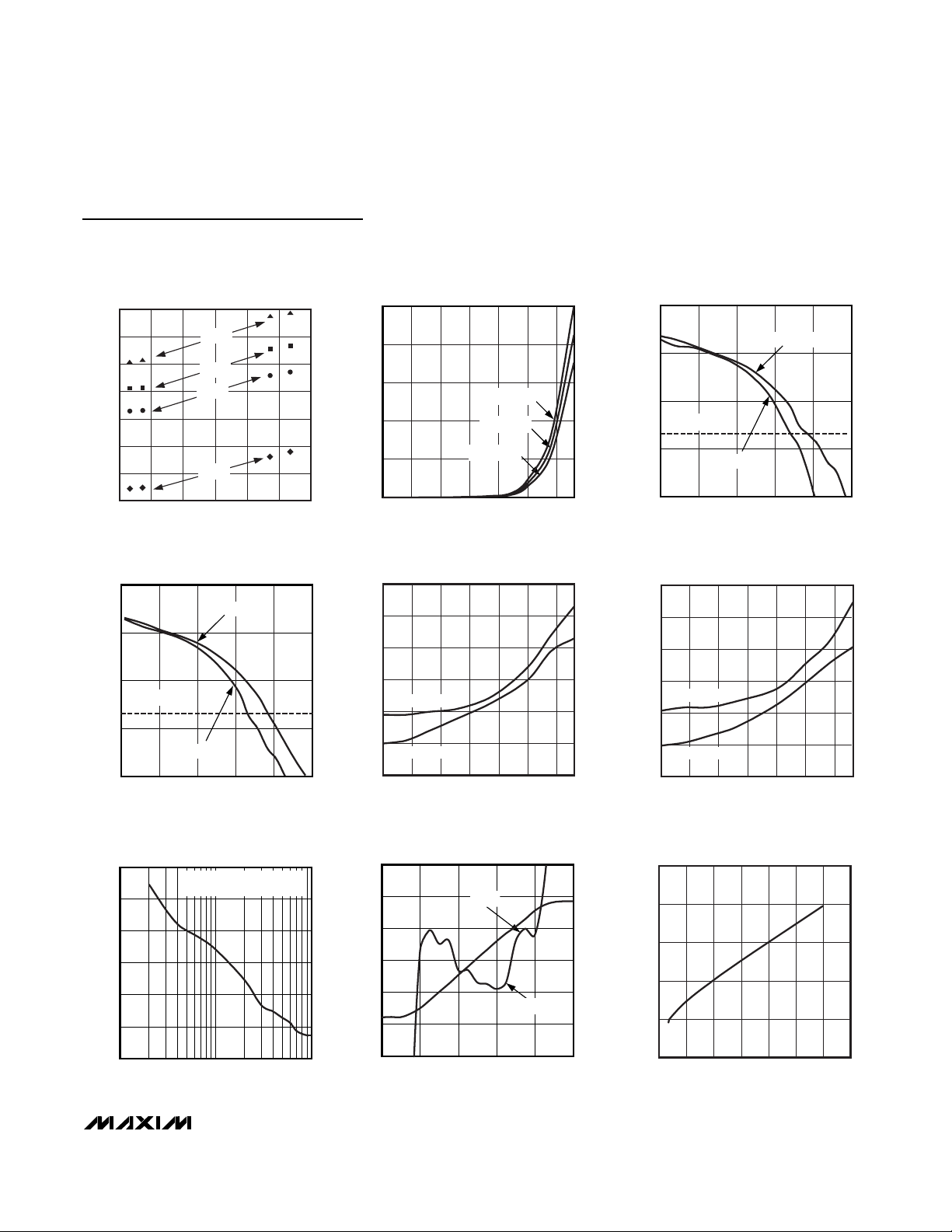
Typical Operating Characteristics
(Typical Application Circuit, VDD= 3.0V, fRF= 433.92MHz, IF BW = 280kHz, data rate = 4kbps Manchester encoded, frequency
deviation = ±50kHz, BER = 0.2%, T
A
= +25°C, unless otherwise noted.)
Operating Frequency f
RSSI Slope 10 16 21 mV/dB
FSK DEMODULATOR
Conversion Gain 1.1 2.1 3.0 mV/kHz
ANALOG BASEBAND
M axi m um P eak- D etector Band w i d th 50 kHz
Maximum Data-Filter Bandwidth BW
Maximum Data-Slicer Bandwidth BW
Maximum Data Rate
CRYSTAL OSCILLATOR
Crystal Frequency f
Crystal Load Capacitance 4.5 pF
PARAMETER SYMBOL CONDITIONS MIN TYP MAX UNITS
IF
DF
DS
10.7 MHz
50 kHz
100 kHz
Manchester coded 33
NRZ 66
XTAL
(fRF - 10.7)
/ 32
kHz
MHz
SUPPLY CURRENT vs. SUPPLY VOLTAGE
7.2
7.0
6.8
6.6
6.4
6.2
6.0
SUPPLY CURRENT (mA)
5.8
5.6
5.4
+85°C
2.4 3.02.7 3.3 3.6
SUPPLY VOLTAGE (V)
(1x I
+125°C
-40°C
LNA
)
+25°C
SUPPLY CURRENT vs. SUPPLY VOLTAGE
(2x I
8.0
7.8
MAX7042 toc01
7.6
7.4
7.2
7.0
6.8
6.6
SUPPLY CURRENT (mA)
6.4
6.2
6.0
+85°C
2.4 3.02.7 3.3 3.6
SUPPLY VOLTAGE (V)
+125°C
LNA
+25°C
)
-40°C
7.0
6.8
MAX7042 toc02
6.6
6.4
6.2
SUPPLY CURRENT (mA)
6.0
5.8
5.6
SUPPLY CURRENT vs. RF FREQUENCY
)
(1x I
LNA
+125°C
+85°C
+25°C
-40°C
300 350 375325 400 425 450
RF FREQUENCY (MHz)
MAX7042 toc03
Page 5
MAX7042
308MHz/315MHz/418MHz/433.92MHz
Low-Power, FSK Superheterodyne Receiver
_______________________________________________________________________________________ 5
Typical Operating Characteristics (continued)
(Typical Application Circuit, VDD= 3.0V, fRF= 433.92MHz, IF BW = 280kHz, data rate = 4kbps Manchester encoded, frequency
deviation = ±50kHz, BER = 0.2%, T
A
= +25°C, unless otherwise noted.)
SUPPLY CURRENT vs. RF FREQUENCY
7.5
7.3
7.1
6.9
6.7
SUPPLY CURRENT (mA)
6.5
6.3
6.1
300 350 375325 400 425 450
RF FREQUENCY (MHz)
(2x I
+125°C
+85°C
+25°C
-40°C
LNA
)
BIT-ERROR RATE vs. AVERAGE INPUT POWER
)
(2x I
100
10
LNA
fRF = 433.92MHz
DEEP-SLEEP CURRENT vs. TEMPERATURE
1000
MAX7042 toc04
800
600
400
DEEP-SLEEP CURRENT (nA)
200
0
-40
TEMPERATURE (°C)
SENSITIVITY vs. TEMPERATURE
(1x I
-103
-104
MAX7042 toc07
-105
VCC = +3.6V
VCC = +3.0V
VCC = +2.4V
)
LNA
BIT-ERROR RATE vs. AVERAGE INPUT POWER
)
(1x I
100
MAX7042 toc05
11085603510-15
10
1
0.2% BER
BIT-ERROR RATE
0.1
0.01
-114 -104
fRF = 315MHz
-112
AVERAGE INPUT POWER (dBm)
LNA
fRF = 433.92MHz
-108-110
-106
SENSITIVITY vs. TEMPERATURE
)
(2x I
LNA
MAX7042 toc08
-106
-107
-108
MAX7042 toc06
MAX7042 toc09
1
0.2% BER
BIT-ERROR RATE
0.1
fRF = 315MHz
0.01
-115
-117 -107
AVERAGE INPUT POWER (dBm)
-109-113 -111
SENSITIVITY
vs. FREQUENCY DEVIATION
-100
-102
-104
-106
SENSITIVITY (dBm)
-108
-110
-112
1100
FREQUENCY DEVIATION IS
MEASURED FROM 0 TO PEAK
10
FREQUENCY DEVIATION (kHz)
MAX7042 toc10
-106
fRF = 433.92MHz
SENSITIVITY (dBm)
-107
-108
fRF = 315MHz
-109
vs. IF INPUT POWER
1.8
1.5
1.2
0.9
RSSI (V)
0.6
0.3
0
-90 -50 -30-70 -10 10
TEMPERATURE (°C)
RSSI AND DELTA
RSSI
RF INPUT POWER (dBm)
DELTA
11085603510-15-40
MAX7042 toc11
-109
SENSITIVITY (dBm)
-110
-111
-112
3
2
1
0
-1
-2
-3
2.0
1.6
1.2
DELTA (%)
0.8
0.4
FSK DEMODULATION OUTPUT (V)
0
10.3 10.5 10.610.4 10.810.7 10.9 11.0
fRF = 433.92MHz
fRF = 315MHz
11085603510-15-40
TEMPERATURE (°C)
FSK DEMODULATOR OUTPUT
vs. IF FREQUENCY
MAX7042 toc12
IF FREQUENCY (MHz)
Page 6
MAX7042
308MHz/315MHz/418MHz/433.92MHz
Low-Power, FSK Superheterodyne Receiver
6 _______________________________________________________________________________________
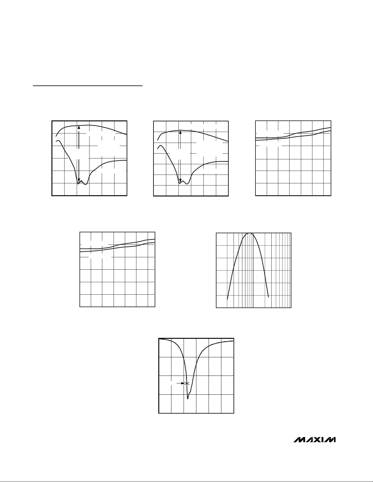
Typical Operating Characteristics (continued)
(Typical Application Circuit, VDD= 3.0V, fRF= 433.92MHz, IF BW = 280kHz, data rate = 4kbps Manchester encoded, frequency
deviation = ±50kHz, BER = 0.2%, T
A
= +25°C, unless otherwise noted.)
SYSTEM GAIN vs. IF FREQUENCY
(1x I
50
40
30
20
SYSTEM GAIN (dB)
10
0
45dB IMAGE
UPPER SIDEBAND
REJECTION
)
LNA
FROM RFIN
TO MIXOUT
= 433.92MHz
f
RF
LOWER SIDEBAND
MAX7042 toc13
SYSTEM GAIN (dB)
SYSTEM GAIN vs. IF FREQUENCY
60
50
40
30
20
10
0
45dB IMAGE
REJECTION
(2x I
LNA
UPPER SIDEBAND
)
FROM RFIN
TO MIXOUT
= 433.92MHz
f
RF
LOWER SIDEBAND
60
50
MAX7042 toc14
40
30
20
IMAGE REJECTION (dB)
10
IMAGE REJECTION vs. TEMPERATURE
(1x I
LNA
fRF = 433.92MHz
fRF = 315MHz
)
MAX7042 toc15
-10
030
IF FREQUENCY (MHz)
252015105
-10
030
IF FREQUENCY (MHz)
IMAGE REJECTION vs. TEMPERATURE
)
(2x I
60
fRF = 433.92MHz
50
fRF = 315MHz
40
30
20
IMAGE REJECTION (dB)
10
0
LNA
MAX7042 toc16
11085603510-15-40
TEMPERATURE (°C)
S11 vs. RF FREQUENCY
0
-4
252015105
NORMALIZED IF GAIN
vs. IF FREQUENCY
0
-3
-6
-9
-12
NORMALIZED IF GAIN (dB)
-15
-18
1
IF FREQUENCY (MHz)
MAX7042 toc18
0
TEMPERATURE (°C)
MAX7042 toc17
10
100
11085603510-15-40
-8
S11 (dB)
433.92MHz
-12
-16
100 1000
RF FREQUENCY (MHz)
850700550400250
Page 7
MAX7042
308MHz/315MHz/418MHz/433.92MHz
Low-Power, FSK Superheterodyne Receiver
_______________________________________________________________________________________ 7
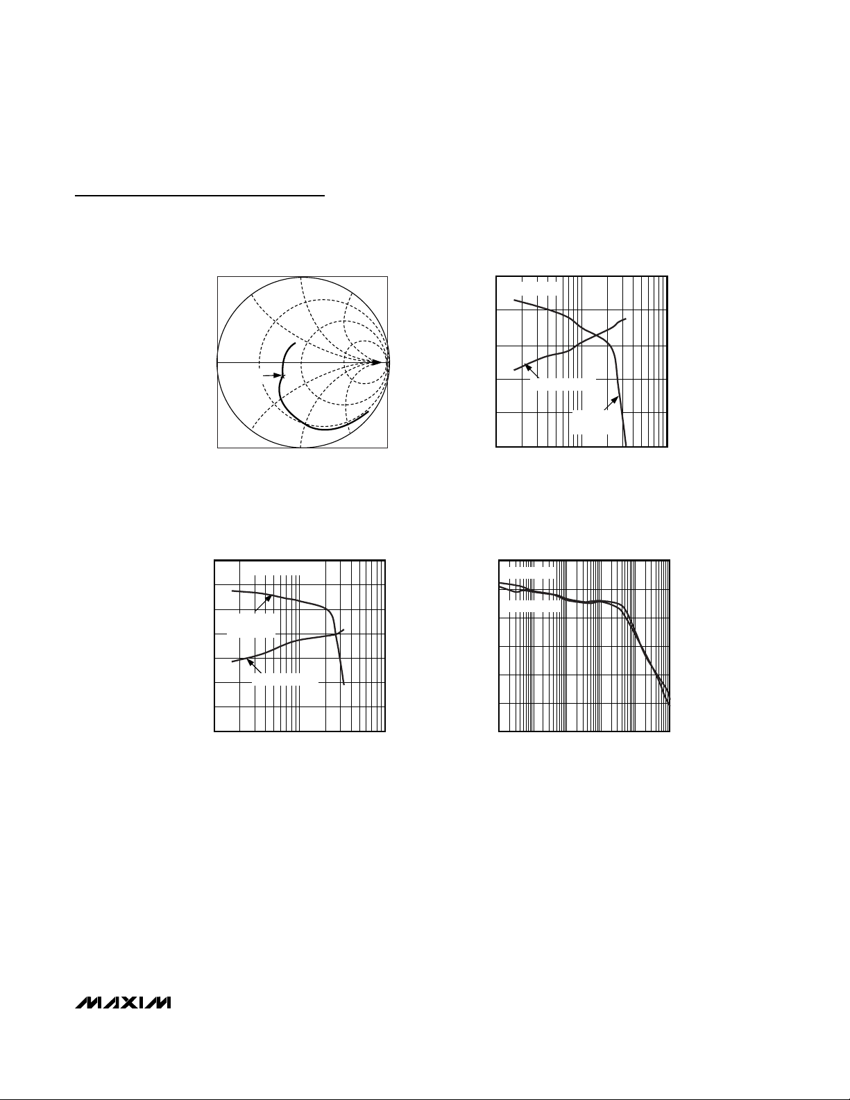
Typical Operating Characteristics (continued)
(Typical Application Circuit, VDD= 3.0V, fRF= 433.92MHz, IF BW = 280kHz, data rate = 4kbps Manchester encoded, frequency
deviation = ±50kHz, BER = 0.2%, T
A
= +25°C, unless otherwise noted.)
433.92MHz
90
80
70
60
50
REAL IMPEDANCE (Ω)
40
30
S11 SMITH PLOT OF R
FIN
INPUT IMPEDANCE
vs. INDUCTIVE DEGENERATION
fRF = 433.92MHz
IMAGINARY
IMPEDANCE
REAL IMPEDANCE
MAX7042 toc21
MAX7042 toc19
-100
-110
-120
-130
IMAGINARY IMPEDANCE (Ω)
INPUT IMPEDANCE
vs. INDUCTIVE DEGENERATION
70
fRF = 315MHz
60
50
40
REAL IMPEDANCE (Ω)
30
20
REAL IMPEDANCE
IMAGINARY
IMPEDANCE
1100
INDUCTIVE DEGENERATION (nH)
10
MAX7042 toc20
-150
-160
-170
-180
-190
-200
IMAGINARY IMPEDANCE (Ω)
PHASE NOISE
vs. OFFSET FREQUENCY
-70
fRF = 315MHz
-80
fRF = 433.92MHz
-90
-100
-110
PHASE NOISE (dBc/Hz)
-120
MAX7042 toc22
20
1100
INDUCTIVE DEGENERATION (nH)
10
-140
-130
100 10k1k 100k 1M 10M
OFFSET FREQUENCY (Hz)
Page 8

MAX7042
308MHz/315MHz/418MHz/433.92MHz
Low-Power, FSK Superheterodyne Receiver
8 _______________________________________________________________________________________
Pin Description
PIN NAME FUNCTION
1, 2 N.C. No Connection. Internally pulled down.
3, 25, 32
N.C. No Connection. Not internally connected.
4 RSSI Buffered Received-Signal-Strength-Indicator Output
5 XTAL2 Crystal Input 2. XTAL2 can be driven from an AC-coupled external reference.
6 XTAL1 Crystal Input 1. Bypass to GND if XTAL2 is driven by an AC-coupled external reference.
7AV
DD
Analog Power-Supply Voltage. AVDD is connected to an on-chip +3.0V regulator in +5V operation.
Bypass AV
DD
to GND with 0.1µF and 220pF capacitors placed as close to the pin as possible.
8 LNAIN Low-Noise Amplifier Input. Must be AC-coupled.
9
Low-Noise Amplifier Source for External Inductive Degeneration. Connect an inductor to GND to set
the LNA input impedance.
10
Low-Noise Amplifier Output. Connect to AVDD through a parallel LC tank filter. AC-couple to MIXIN+.
11 MIXIN+ Noninverting Mixer Input. Must be AC-coupled to the LNA output.
12 MIXIN- Inverting Mixer Input. Bypass to AVDD or AGND with a capacitor.
13 MIXOUT 330Ω Mixer Output. Connect to the input of the 10.7MHz IF filter.
14 AGND Analog Ground
15 IFIN- Inverting 330Ω IF Limiter Amplifier Input. Bypass to AGND with a capacitor.
16 IFIN+ Noninverting 330Ω IF Limiter Amplifier Input. Connect to the output of the 10.7MHz IF filter.
17 PDMIN Minimum-Level Peak Detector for Demodulator Output
18 PDMAX Maximum-Level Peak Detector for Demodulator Output
19 DS- Inverting Data-Slicer Input
20 DS+ Noninverting Data-Slicer Input
21 OP+ Noninverting Op-Amp Input for the Sallen-Key Data Filter
22 DF Data-Filter Feedback Node. Input for the feedback of the Sallen-Key data filter.
23 DGND Digital Ground
24 DV
DD
Digital Power-Supply Voltage. Bypass to DGND with 0.01µF and 220pF capacitors placed as close to
the pin as possible.
26 EN
Enable. Internally pulled down. Drive high for normal operation. Drive low or leave unconnected to put
the device into shutdown mode.
27 FSEL1 Frequency-Select Pin 1 (see Table 1). Internally pulled down. Connect to EN for logic-high operation.
28 FSEL2 Frequency-Select Pin 2 (see Table 1). Internally pulled down. Connect to EN for logic-high operation.
29 HV
IN
High-Voltage Supply Input. For +3V operation, connect HVIN to AVDD and DVDD. For +5V operation,
connect only HV
IN
to +5V. Bypass HVIN to AGND with 0.01µF and 220pF capacitors placed as close
to the pin as possible.
30 DATA Receiver Data Output
31 LNASEL
LNA Bias Current Select Pin. Internally pulled down. Set LNASEL to logic-low for low LNA current and
set LNASEL to logic-high for high LNA current. Connect to EN for logic-high operation.
EP GND Exposed Paddle. Connect to ground.
LNASRC
LNAOUT
Page 9

MAX7042
308MHz/315MHz/418MHz/433.92MHz
Low-Power, FSK Superheterodyne Receiver
_______________________________________________________________________________________ 9
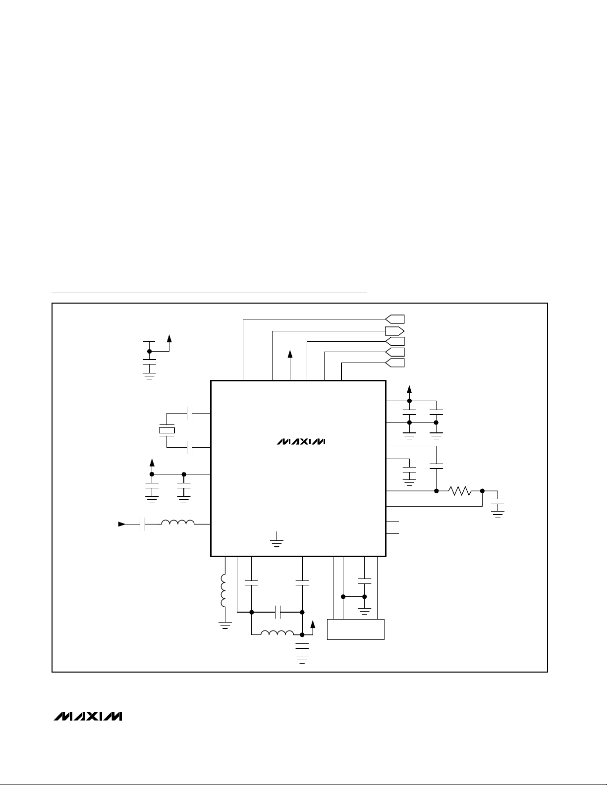
Functional Diagram
LNAIN
LNASRC
AGND
XTAL1
XTAL2
DV
LNAOUT MIXIN+ MIXIN-
10
8
9
14
6
5
26
EN
24
DD
LNA
CRYSTAL
OSCILLATOR
EXPOSED
PADDLE*
DIVIDE-
BY-32
PHASE
DETECTOR
11 12 13 15 16
IMAGE
REJECTION
0˚
Σ
90˚
VCO
FSK
LOOP
FILTER
MAX7042
R
DF1
100kΩ
R
DF2
100kΩ
IFIN-
MIXOUT IFIN+
RSSI
FSK
DEMODULATOR
IF LIMITING
AMPS
4
RSSI
FSEL1
27
FSEL2
28
23
DGND
29
HV
IN
7
AV
DD
*MUST BE CONNECTED TO AGND.
3.0V
REG
3.0V
FSK
DATA
FILTER
19 18 17 20 21 22
30
LNASEL
31
DFOP+DS+PDMAXDS-DATA PDMIN
Page 10

MAX7042
308MHz/315MHz/418MHz/433.92MHz
Low-Power, FSK Superheterodyne Receiver
10 ______________________________________________________________________________________
Detailed Description
The MAX7042 CMOS superheterodyne receiver and a
few external components provide a complete FSK
receive chain from the antenna to the digital output
data. FSK uses the difference in frequency of the carrier to represent a logic 0 and logic 1. Depending on signal power and component selection, data rates as high
as 66kbps NRZ can be achieved.
Frequency Selection
The MAX7042 can be tuned to one of four frequencies
using the 2 frequency-select bits FSEL1 and FSEL2:
308, 315, 418, and 433.92MHz, as shown in Table 1.
The LO frequencies are 32 times the reference crystal
frequencies of 9.29063, 9.50939, 12.72813, and
13.22563MHz. The selected crystal frequency is used
to calibrate the FSK detector PLL so that it operates at
the middle of the 10.7MHz IF.
Low-Noise Amplifier (LNA)
The LNA is a cascode amplifier with off-chip inductive
degeneration. The gain and the noise figure are dependent on both the antenna matching network at the LNA
input and the LC tank network between the LNA output
and the mixer input.
The MAX7042 allows for user programmability of the
LNA bias current. Input LNASEL programs 1x to 2x
bias currents in increments of 0.6mA from 0.6mA to
1.2mA. Setting LNASEL to logic-low programs the LNA
to consume 1x bias current and setting LNASEL to
logic-high programs the LNA to consume 2x bias current. Larger bias currents yield better sensitivity and
gain at the expense of current drain.
The off-chip inductive degeneration is achieved by
connecting an inductor from LNASRC to AGND. This
inductor sets the real part of the input impedance at
LNAIN, allowing for a more flexible match to a low-input
impedance such as a PC board trace antenna. A nominal
value of this inductor for a 50Ω input impedance is 3.9nH
at 315MHz and 0nH (short) at 433.92MHz, but is affected
by the PC board trace. See the Typical Operating
Characteristics for the relationship between the inductance and input impedance.
The LC tank filter connected to LNAOUT consists of L2
and C9 (see the Typical Application Circuit). Select L2
and C9 to resonate at the desired RF input frequency.
The resonant frequency is given by:
where L
TOTAL
= L2 + L
PARASITICS
and C
TOTAL
= C9 +
C
PARASITICS
.
L
PARASITICS
and C
PARASITICS
include inductance and
capacitance of the PC board traces, package pins,
mixer input impedance, LNA output impedance, etc.
These parasitics at high frequencies cannot be ignored,
and can have a dramatic effect on the tank filter center
frequency. Lab experimentation is required to optimize
the center frequency of the tank. The parasitic capacitance is generally 5pF to 7pF.
There are two ways to verify experimentally that the resonant frequency of the tank is centered at the desired
RF frequency:
1) Drive the crystal oscillator externally and sweep both
the RF frequency and the LO frequency (FXTAL x
32) to keep the IF at 10.7MHz while monitoring the
RSSI voltage (pin 4). There is a peak in the RSSI
voltage at resonance. The external source must be
AC-coupled into XTAL1 and the XTAL2 pin must
have an AC bypass to ground. The recommended
drive power is -10dBm.
2) Use a network analyzer to measure the resonance.
The port 1 power from the network analyzer is input
to the receiver, and this power must be -30dBm or
less. A coaxial stub with the center conductor
exposed (commonly called an RF “sniffer” is used to
monitor the tank power and serves as the port 2
input to the network analyzer. The sniffer should be
placed in close proximity to, but not actually touching, the tank inductor.
Table 1. Frequency Selection Table
FSEL2 FSEL1
0 0 308
0 1 315
1 0 418
1 1 433.92
FREQUENCY
(MHz)
f
=
2π
1
LxC
TOTAL TOTAL
Page 11

MAX7042
308MHz/315MHz/418MHz/433.92MHz
Low-Power, FSK Superheterodyne Receiver
______________________________________________________________________________________ 11
Mixer
A unique feature of the MAX7042 is the integrated image
rejection of the mixer. This device is designed to eliminate the need for a costly front-end SAW filter in many
applications. The advantages of not using a SAW filter
are increased sensitivity, simplified antenna matching,
less board space, and lower cost.
The mixer cell is a pair of double-balanced mixers that
perform an IQ downconversion of the RF input to the
10.7MHz intermediate frequency (IF) with low-side
injection (i.e., fLO= fRF- fIF). The image-rejection circuit
then combines these signals to achieve a typical image
rejection of approximately 45dB. Low-side injection is
required as high-side injection is not possible due to
the on-chip image rejection. The IF output is driven by
a source follower, biased to create a driving impedance of 330Ω to interface with an off-chip 330Ω ceram-
ic IF filter. Note that MIXIN+ and MIXIN- are functionally
identical.
Phase-Locked Loop (PLL)
The PLL block contains a phase detector, charge
pump/integrated loop filter, voltage-controlled oscillator
(VCO), asynchronous 32x frequency divider, and crystal oscillator. This PLL does not require any external
components. The relationship between the RF, IF, and
reference frequencies is given by:
To allow the smallest possible IF bandwidth (for best
sensitivity), minimize the tolerance of the reference.
Intermediate Frequency (IF)
The IF section presents a differential 330Ω load to provide matching for the off-chip ceramic filter. The internal six AC-coupled limiting amplifiers produce an
overall gain of approximately 65dB. The limiting amplifiers have a bandpass-filter-type response centered
near the 10.7MHz IF frequency with a 3dB bandwidth
of approximately 10MHz. The limiter output is fed into a
PLL to demodulate the IF, producing a baseband voltage with a demodulation slope of 2.1mV/kHz. The RSSI
circuit produces a DC output proportional to the log of
the IF signal level with a slope of approximately
16mV/dB.
FSK Demodulator
The FSK demodulator uses an integrated 10.7MHz PLL
that tracks the input RF modulation and determines the
difference between frequencies as logic ones and
zeros. The PLL is illustrated in Figure 1. The input to the
PLL comes from the output of the IF limiting amplifiers.
The PLL control voltage responds to changes in the frequency of the input signal with a nominal gain of
2.1mV/kHz. For example, an FSK peak-to-peak deviation of 50kHz generates a 105mV
P-P
signal on the control line. This control line is then filtered and sliced by
the FSK baseband circuitry.
The FSK demodulator PLL requires calibration to overcome variations in process, voltage, and temperature.
The maximum calibration time is 120µs, which is included in the startup time. Recalibration is necessary after a
significant change in temperature or supply voltage.
Calibration occurs automatically each time the
MAX7042 is powered up. Drive EN low and then high to
force a recalibration.
Figure 1. FSK Demodulator PLL Block Diagram
IF
LIMITING
AMPS
PHASE
DETECTOR
CHARGE
PUMP
TO FSK
BASEBAND FILTER
AND DATA SLICER
LOOP
FILTER
10.7MHz VCO
2.1mV/kHz
ff
( )
−
=
RF IF
32
f
REF
Page 12

MAX7042
308MHz/315MHz/418MHz/433.92MHz
Low-Power, FSK Superheterodyne Receiver
12 ______________________________________________________________________________________
Crystal Oscillator
The XTAL oscillator in the MAX7042 is used to generate
the LO for mixing with the received signal. The XTAL oscillator frequency sets the received signal frequency as:
f
RECEIVE
= (f
XTAL
x 32) + 10.7MHz
The received image frequency at:
f
IMAGE
= (f
XTAL
x 32) - 10.7MHz
is suppressed by the integrated quadrature imagerejection circuitry.
The XTAL oscillator in the MAX7042 is designed to present a capacitance of approximately 3pF between
XTAL1 and XTAL2. In most cases, this corresponds to a
4.5pF load capacitance applied to the external crystal
when typical PC board parasitics are added. It is very
important to use a crystal with a load capacitance that is
equal to the capacitance of the MAX7042 crystal oscillator plus PC board parasitics. If a crystal designed to
oscillate with a different load capacitance is used, the
crystal is pulled away from its intended operating frequency, introducing an error in the reference frequency.
Crystals designed to operate with higher differential load
capacitance always pull the reference frequency higher.
In reality, the oscillator pulls every crystal. A crystal’s natural frequency is really below its specified frequency, but
when loaded with the specified load capacitance, the
crystal is pulled and oscillates at its specified frequency.
This pulling is accounted for in the specification of the
load capacitance.
Additional pulling can be calculated if the electrical
parameters of the crystal are known. The frequency
pulling is given by:
where:
f
p
is the amount the crystal frequency is pulled in ppm.
Cmis the motional capacitance of the crystal.
C
case
is the case capacitance.
C
spec
is the specified load capacitance.
C
load
is the actual load capacitance.
When the crystal is loaded as specified, i.e., C
load
=
C
spec
, the frequency pulling equals zero.
Frequency Tolerance
The frequency tolerance of the crystal, the frequency
and bandwidth tolerance of the IF filter, and the desired
modulation bandwidth of the signal are all interrelated.
The combination of these characteristics should be such
to ensure that the modulated signal bandwidth stays
within the passband of the IF filter after downconversion.
As is shown below, a 50ppm tolerance crystal in combination with a 280kHz bandwidth IF filter is sufficient for
most FSK-modulated signals.
Smaller IF filter bandwidths can be used if high-tolerance
crystals are used for generating both transmitter and
MAX7042 receiver PLL references. The modulated spectrum of the transmitted signal must be downconverted by
the MAX7042 to fall within the passband of the IF filter.
The crystal tolerances must take into account the initial
+25°C tolerance, aging, load capacitance tolerances,
and temperature drift for both the transmitter and
MAX7042 receiver. To achieve acceptable signal reception, the following equation must hold:
2 x (∆F
TX
+ ∆FRX+ ∆FIF+ F
DEV
+ 5 x F
MOD
) < IFBW
min
where:
∆FTX= (transmitter crystal tolerance in ppm) x (carrier
frequency in MHz). This includes aging, load capacitance, and temperature effects for the crystal tolerance.
∆FRX= (MAX7042 crystal tolerance in ppm) x (carrier
frequency in MHz). This includes aging, load capacitance, and temperature effects for the crystal tolerance.
∆FIF= The center frequency tolerance of the selected
IF filter. This includes temperature drift of the IF filter
center frequency.
F
DEV
= ±FSK frequency deviation from carrier frequency.
F
MOD
= One half of NRZ data rate, or the data rate if
Manchester coding is used.
IFBW
min
= The minimum bandwidth of the selected IF
filter.
As an example, assume 315MHz carrier frequency,
±50ppm crystal tolerances for both transmitter and
MAX7042, ±30kHz IF filter center frequency tolerance,
±50kHz frequency deviation, and 4.8kHz Manchester
data rate:
2 x [(315 x 50) + (315 x 50) + 30000 +50000 + 5 x
4800] = 271kHz < IFBW
min
This operating condition necessitates a 280kHz IF filter.
f
p
⎛
C
m
=
⎜
2
⎝
11
+
CC CC
case load case spec
−
+
⎞
⎟
⎠
x
10
6
Page 13

MAX7042
308MHz/315MHz/418MHz/433.92MHz
Low-Power, FSK Superheterodyne Receiver
______________________________________________________________________________________ 13
Data Filters
The data filter is implemented as a 2nd-order lowpass
Sallen-Key filter. The pole locations are set by the combination of two on-chip resistors and two external
capacitors. Adjusting the value of the external capacitors changes the corner frequency to optimize for different data rates. The corner frequency in kHz should
be to approximately the fastest expected data rate in
kbps for NRZ and twice the fastest expected data rate
in kbps for Manchester coding from the transmitter.
Keeping the corner frequency near the data rate
rejects any noise at higher frequencies, resulting in an
increase in receiver sensitivity.
The configuration shown in Figure 2 creates a Butterworth
or Bessel response. The Butterworth filter offers a very
flat amplitude response in the passband and a rolloff rate
of 40dB/decade for the two-pole filter. The Bessel filter
has a linear phase response, which works well for filtering digital data. To calculate the value of the capacitors,
use the following equations along with the coefficients in
Table 2:
where f
C
is the desired 3dB corner frequency.
For example, choose a Butterworth filter response with
a 5kHz corner frequency:
Choosing standard capacitor values changes CF1to
470pF and CF2to 220pF. In the Typical Application
Circuit, CF1and CF2are named C4 and C3, respectively.
Data Slicer
The purpose of a data slicer is to take the analog output
of a data filter and convert it to a digital signal. This is
achieved by using a comparator and comparing the analog input to a threshold voltage. The threshold voltage is
set by the voltage on the DS- pin, which is connected to
the negative input of the data-slicer comparator. The positive input of the data-slicer comparator is connected to
the output of the data filter internally.
Table 2. Coefficients to Calculate CF1and
C
F2
Figure 2. Sallen-Key Lowpass Data Filter
C
C
F
1
F
2
=
=
b
100
()()()
ΩΩπ
ak f
C
a
4 100
()()()
π
kf
C
FILTER TYPE a b
Butterworth
(Q = 0.707)
Bessel
(Q = 0.577)
MAX7042
DS+ OP+
1.414 1.000
1.3617 0.618
FSK DEMOD
100kΩ
C
F2
100kΩ
DF
C
F1
1 000
C
=≈
FF1
1 414 100 3 14 5
( . )( )( . )( )
C
=≈
2
4 100 3 14 5
( )( )( . )( )
.
k kHz
Ω
1 414
.
k kHz
Ω
225
450
pF
pF
Page 14

MAX7042
308MHz/315MHz/418MHz/433.92MHz
Low-Power, FSK Superheterodyne Receiver
14 ______________________________________________________________________________________
Numerous configurations can be used to generate the
data-slicer threshold. For example, the circuit in Figure 3
shows a simple method using only one resistor and one
capacitor. This configuration averages the analog output of the filter and sets the threshold to approximately
50% of that amplitude. With this configuration, the
threshold automatically adjusts as the analog signal
varies, minimizing the possibility for errors in the digital
data. The values of R and C affect how fast the threshold tracks the analog amplitude. Be sure to keep the
corner frequency of the RC circuit much lower than the
lowest expected data rate.
With this configuration, a long string of zeros or ones
can cause the threshold to drift. This configuration
works best if a coding scheme, such as Manchester
coding, which has an equal number of zeros and ones,
is used.
Figure 4 shows a configuration that uses the positive and
negative peak detectors to generate the threshold. This
configuration sets the threshold to the midpoint between
a high output and a low output of the data filter.
Peak Detectors
The maximum peak detector (PDMAX) and minimum
peak detector (PDMIN) outputs, in conjunction with a
resistor and capacitor connected to GND, create DC
output voltages proportional to the high- and low-peak
values of the data signal. The resistor provides a path
for the capacitor to discharge, allowing the peak detector to dynamically follow peak changes of the data-filter
output voltage.
The positive and negative peak detectors can be used
together to form a data-slicer threshold voltage at a
midvalue between the most positive and most negative
voltage levels of the data stream (see the Data Slicers
section and Figure 4). Set the RC time constant of the
peak-detector combining network to at least 5 times the
data period.
The MAX7042 peak detectors track the baseband filter
output voltage until all internal circuits are stable following an enable pin low-to-high transition. This feature
allows for an extremely fast startup because the peak
detectors never “catch” a false level created by a startup
transient. The peak detectors exhibit a fast-attack/slowdecay response.
Power-Supply Connections
The MAX7042 can be powered from a 2.4V to 3.6V
supply or a 4.5V to 5.5V supply. The device has an on-
chip linear regulator that reduces the 5V supply to 3V
needed to operate the chip.
To operate the MAX7042 from a 3V supply, connect
DVDD, AVDD, and HVINto the 3V supply. When using a
5V supply, connect the supply to HVINonly. In both
cases, bypass DVDDand HVINwith a 0.01µF capacitor
and AVDDwith a 0.1µF capacitor. Place all bypass
capacitors as close to the respective supply pin as
possible.
Figure 3. Generating Data-Slicer Threshold
Figure 4. Generating Data-Slicer Threshold Using the Peak
Detectors
DATA PDMAX PDMIN
MAX7042
DATA DS-
MAX7042
DATA
SLICER
DATA
SLICER
R
C
PEAK
DET
RR
CC
DS+
PEAK
DET
Page 15
MAX7042
308MHz/315MHz/418MHz/433.92MHz
Low-Power, FSK Superheterodyne Receiver
______________________________________________________________________________________ 15
Layout Considerations
A properly designed PC board is an essential part of
any RF/microwave circuit. On high-frequency inputs
and outputs, use controlled-impedance lines and keep
them as short as possible to minimize losses and radiation. At high frequencies, trace lengths that are on the
order of λ/10 or longer act as antennas.
Keeping the traces short also reduces parasitic inductance. Generally, 1in of a PC board trace adds about
20nH of parasitic inductance. The parasitic inductance
can have a dramatic effect on the effective inductance
of a passive component. For example, a 0.5in trace
connecting a 100nH inductor adds an extra 10nH of
inductance or 10%.
To reduce the parasitic inductance, use wider traces
and a solid ground or power plane below the signal
traces. Also, use low-inductance connections to ground
on all GND pins, and place decoupling capacitors
close to all V
DD
or HVINconnections.
Typical Application Circuit
V
DD
3.0V
C16
31 30 29 28 27 26
DATA
LNASEL
EXPOSED PADDLE
RF INPUT
C6
C7
Y1
V
4
C14
C15
DD
C13
L1
RSSI
5
XTAL2
6
XTAL1
7
AV
DD
8
LNAIN
LNASEL
DATA
V
DD
IN
HV
MAX7042
FSEL2
FSEL1
EN
DV
DD
DGND
DF
OP+
DS+
DS-
PDMAX
PDMIN
FSEL2
FSEL1
EN
V
DD
24
C3
C2C1
C4
R1
23
22
21
20
19
18
17
C5
LNASRC
910 11 12 1314 15
L3
MIXIN+
LNAOUT
C11 C8
C9
L2
MIXIN-
C10
MIXOUT
AGND
IFIN-
IFIN+
16
C12
V
DD
GNDY2OUTIN
Page 16

MAX7042
308MHz/315MHz/418MHz/433.92MHz
Low-Power, FSK Superheterodyne Receiver
16 ______________________________________________________________________________________
Chip Information
PROCESS: CMOS
Table 3. Component Values for Typical Application Circuit
COMPONENT
C1 0.01µF 0.01µF 5%
C2 220pF 220pF 5%
C3 220pF 220pF 5%
C4 470pF 470pF 5%
C5 0.047µF 0.047µF 10%
C6 0.1µF 0.1µF 10%
C7 100pF 100pF 10%
C8 100pF 100pF 10%
C9 1.2pF Open ±0.1pF
C10 220pF 220pF 10%
C11 100pF 100pF 10%
C12 1500pF 1500pF 10%
C13 220pF 220pF 10%
C14 100pF 100pF 10%
C15 100pF 100pF 10%
C16 0.1µF 0.1µF 10%
L1 82nH 39nH Coilcraft 0603CS
L2 30nH 16nH Murata LQW18A
L3 3.9nH Short Coilcraft 0603CS
R1 100kΩ 100kΩ 5%
Y1 9.50939MHz 13.22563MHz Crystal
Y2 10.7MHz ceramic filter 10.7MHz ceramic filter Murata SFECV10.7 series
VALUE FOR
315MHz RF
VALUE FOR
433.92MHz RF
DESCRIPTION
Page 17
MAX7042
308MHz/315MHz/418MHz/433.92MHz
Low-Power, FSK Superheterodyne Receiver
______________________________________________________________________________________ 17
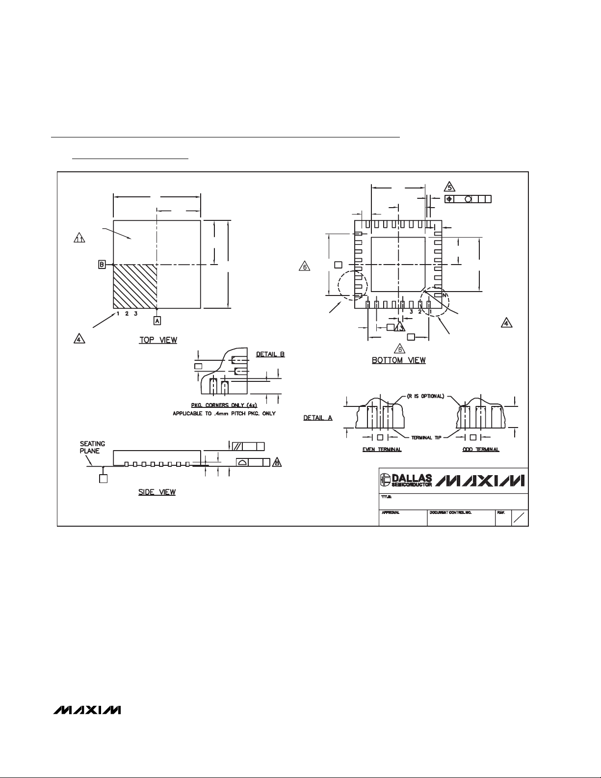
Package Information
(The package drawing(s) in this data sheet may not reflect the most current specifications. For the latest package outline information,
go to www.maxim-ic.com/packages
.)
D/2
D2
b
C
L
k
E/2
E
e
L
L1
(NE-1) X e
DETAIL A
D2/2
e/2
e
(ND-1) X e
L
0.10 M C A B
L
E2/2
PIN # 1 I.D.
DETAIL B
C
E2
L
0.35x45°
CC
L
LL
D
MARKING
XXXXX
PIN # 1
I.D.
QFN THIN.EPS
C
-DRAWING NOT TO SCALE-
0.10 C
A
0.08 C
A3
A1
e e
PACKAGE OUTLINE,
16, 20, 28, 32, 40L THIN QFN, 5x5x0.8mm
21-0140
1
H
2
Page 18
MAX7042
308MHz/315MHz/418MHz/433.92MHz
Low-Power, FSK Superheterodyne Receiver
Maxim cannot assume responsibility for use of any circuitry other than circuitry entirely embodied in a Maxim product. No circuit patent licenses are
implied. Maxim reserves the right to change the circuitry and specifications without notice at any time.
18 ____________________Maxim Integrated Products, 120 San Gabriel Drive, Sunnyvale, CA 94086 408-737-7600
© 2005 Maxim Integrated Products Printed USA is a registered trademark of Maxim Integrated Products, Inc.
Package Information (continued)
(The package drawing(s) in this data sheet may not reflect the most current specifications. For the latest package outline information,
go to www.maxim-ic.com/packages
.)
PKG.
SYMBOL
A1
A3
ND
NE
JEDEC
NOTES:
1. DIMENSIONING & TOLERANCING CONFORM TO ASME Y14.5M-1994.
2. ALL DIMENSIONS ARE IN MILLIMETERS. ANGLES ARE IN DEGREES.
3. N IS THE TOTAL NUMBER OF TERMINALS.
4. THE TERMINAL #1 IDENTIFIER AND TERMINAL NUMBERING CONVENTION SHALL
CONFORM TO JESD 95-1 SPP-012. DETAILS OF TERMINAL #1 IDENTIFIER ARE
OPTIONAL, BUT MUST BE LOCATED WITHIN THE ZONE INDICATED. THE TERMINAL #1
IDENTIFIER MAY BE EITHER A MOLD OR MARKED FEATURE.
5. DIMENSION b APPLIES TO METALLIZED TERMINAL AND IS MEASURED BETWEEN
0.25 mm AND 0.30 mm FROM TERMINAL TIP.
6. ND AND NE REFER TO THE NUMBER OF TERMINALS ON EACH D AND E SIDE RESPECTIVELY.
7. DEPOPULATION IS POSSIBLE IN A SYMMETRICAL FASHION.
8. COPLANARITY APPLIES TO THE EXPOSED HEAT SINK SLUG AS WELL AS THE TERMINALS.
9. DRAWING CONFORMS TO JEDEC MO220, EXCEPT EXPOSED PAD DIMENSION FOR T2855-1,
T2855-3, AND T2855-6.
10. WARPAGE SHALL NOT EXCEED 0.10 mm.
11. MARKING IS FOR PACKAGE ORIENTATION REFERENCE ONLY.
12. NUMBER OF LEADS SHOWN ARE FOR REFERENCE ONLY.
13. LEAD CENTERLINES TO BE AT TRUE POSITION AS DEFINED BY BASIC DIMENSION "e", ±0.05.
-DRAWING NOT TO SCALE-
MIN. MAX.NOM.
A
0.70 0.800.75
b
0.25
4.90
D
E
4.90
e
0.250--
k
L
0.30 0.500.40
---
L1
N
16L 5x5
0.02
0.20 REF.
5.00
0.80 BSC.
16
4
4
WHHB
COMMON DIMENSIONS
20L 5x5
NOM.
MIN.
MAX.
0.70
0.80
0.75
0.05
0
0.05
0.02
0.20 REF.
0.350.30
0.30
0.25
4.90
4.90
0.25
0.45
---
5.00
5.00
0.65 BSC.
0.55
20
5
5
WHHC
0.35
5.10
5.10
0.65
5.10
5.105.00
--
28L 5x5
MIN.
0.70
0
0.20 REF.
0.20
4.90
4.90
0.50 BSC.
0.25
0.45
---
WHHD-1
NOM.
0.75
0.02
0.25
5.00
5.00
0.55
28
7
7
MAX.
MIN.
0.80
0.70
0.05
0.20 0.25 0.30
0.30
4.90
5.10
4.90
5.10
0.25
--
0.30
0.65
32L 5x5
NOM.
0.75
0
0.02
0.20 REF.
5.00
5.00
0.50 BSC.
0.40
---
32
WHHD-2
8
8
MAX.
MIN.
0.80
0.70
0.05
0.15
5.10
4.90
5.10
4.90 5.00
--
0.25 0.35 0.45
0.50
0.30
40L 5x5
NOM.
0.75 0.80
0.20 REF.
5.00 5.10
0.40 BSC.
0.40 0.50
40
10
10
-----
MAX.
0.0500.02
0.250.20
5.10
0.600.40 0.50
EXPOSED PAD VARIATIONS
PKG.
CODES
D2
MAX.
NOM.MIN.
MIN.E2NOM. MAX.
T1655-1 3.203.00 3.10 3.00 3.10 3.20
3.203.00T1655-2 3.10 3.00 3.10 3.20 YE S
3.00T2055-2 3.10
3.20
3.203.00 3.10
3.103.00 3.203.103.00 3.20T2055-4
3.353.15T2055-5 3.25 3.15 3.25 3.35
3.353.15T2855-1 3.25 3.353.15 3.25
T2855-2 2.60 2.602.80 2.70 2.80
2.70
T2855-3 3.15 3.25 3.35 3.15 3.25 3.35
T2855-4 2.60 2.70 2.80 2.60 2.70 2.80
T2855-5 2.60 2.70 2.80 2.60 2.70 2.80
T2855-6 3.15 3.25 3.35 3.15 3.25 3.35
3.10
2.80
2.60 2.70 2.80
3.35
3.35
3.20
3.00 3.10 3.20
T2855-7 2.60 2.70
3.15T2855-8 3.25 3.15 3.25 3.35
3.15T2855N-1 3.25 3.15 3.25 3.35
T3255-2
3.00
3.203.00 3.10T3255-3 3.203.00 3.10
3.203.00 3.10T3255-4 3.203.00 3.10
3.203.10T3255N-1 3.00
3.203.103.00
3.30T4055-1 3.20 3.40 3.20 3.30 3.40
SEE COMMON DIMENSIONS TABLE
**
PACKAGE OUTLINE,
16, 20, 28, 32, 40L THIN QFN, 5x5x0.8mm
21-0140
±0.15
0.40
0.40
DOWN
L
BONDS
ALLOWED
NO
**
**
NO3.203.103.003.10T1655N-1 3.00 3.20
**
NO
**
YES3.103.00 3.203.103.00 3.20T2055-3
**
NO
**
YES
NO
**
NO
**
YES
**
YES
**
NO
**
NO
**
YES
**
YES
NO
**
NO
**
YES
**
NO
**
NO
**
YES
**
2
H
2
 Loading...