

Page 1

General Description
The MAX7032 crystal-based, fractional-N transceiver is
designed to transmit and receive ASK/OOK or FSK
data in the 300MHz to 450MHz frequency range with
data rates up to 33kbps (Manchester encoded) or
66kbps (NRZ encoded). This device generates a typical output power of +10dBm into a 50Ω load, and
exhibits typical sensitivities of -114dBm for ASK data
and -110dBm for FSK data. The MAX7032 features separate transmit and receive pins (PAOUT and LNAIN)
and provides an internal RF switch that can be used to
connect the transmit and receive pins to a common
antenna.
The MAX7032 transmit frequency is generated by a 16bit, fractional-N, phase-locked loop (PLL), while the
receiver’s local oscillator (LO) is generated by an integer-N PLL. This hybrid architecture eliminates the need
for separate transmit and receive crystal reference
oscillators because the fractional-N PLL allows the
transmit frequency to be set within 2kHz of the receive
frequency. The 12-bit resolution of the fractional-N PLL
allows frequency multiplication of the crystal frequency
in steps of f
XTAL
/ 4096. Retaining the fixed-N PLL for
the receiver avoids the higher current drain requirements of a fractional-N PLL and keeps the receiver current drain as low as possible.
The fractional-N architecture of the MAX7032 transmit
PLL allows the transmit FSK signal to be programmed for
exact frequency deviations, and completely eliminates
the problems associated with oscillator-pulling FSK signal generation. All frequency-generation components are
integrated on-chip, and only a crystal, a 10.7MHz IF filter,
and a few discrete components are required to implement a complete antenna/digital data solution.
The MAX7032 is available in a small 5mm x 5mm, 32-pin,
thin QFN package, and is specified to operate in the
automotive -40°C to +125°C temperature range.
Applications
2-Way Remote Keyless Entry
Security Systems
Home Automation
Remote Controls
Remote Sensing
Smoke Alarms
Garage Door Openers
Local Telemetry Systems
Features
♦ +2.1V to +3.6V or +4.5V to +5.5V Single-Supply
Operation
♦ Single Crystal Transceiver
♦ User-Adjustable 300MHz to 450MHz Carrier
Frequency
♦ ASK/OOK and FSK Modulation
♦ User-Adjustable FSK Frequency Deviation
Through Fractional-N PLL Register
♦ Agile Transmitter Frequency Synthesizer with
f
XTAL
/ 4096 Carrier-Frequency Spacing
♦ +10dBm Output Power into 50Ω Load
♦ Integrated TX/RX Switch
♦ Integrated Transmit and Receive PLL, VCO, and
Loop Filter
♦ > 45dB Image Rejection
♦ Typical RF Sensitivity*
ASK: -114dBm
FSK: -110dBm
♦ Selectable IF Bandwidth with External Filter
♦ RSSI Output with High Dynamic Range
♦ Autopolling Low-Power Management
♦ < 12.5mA Transmit-Mode Current
♦ < 6.7mA Receive-Mode Current
♦ < 23.5µA Polling-Mode Current
♦ < 800nA Shutdown Current
♦ Fast-On Startup Feature, < 250µs
♦ Small 32-Pin, Thin QFN Package
MAX7032
Low-Cost, Crystal-Based, Programmable,
ASK/FSK Transceiver with Fractional-N PLL
________________________________________________________________ Maxim Integrated Products 1
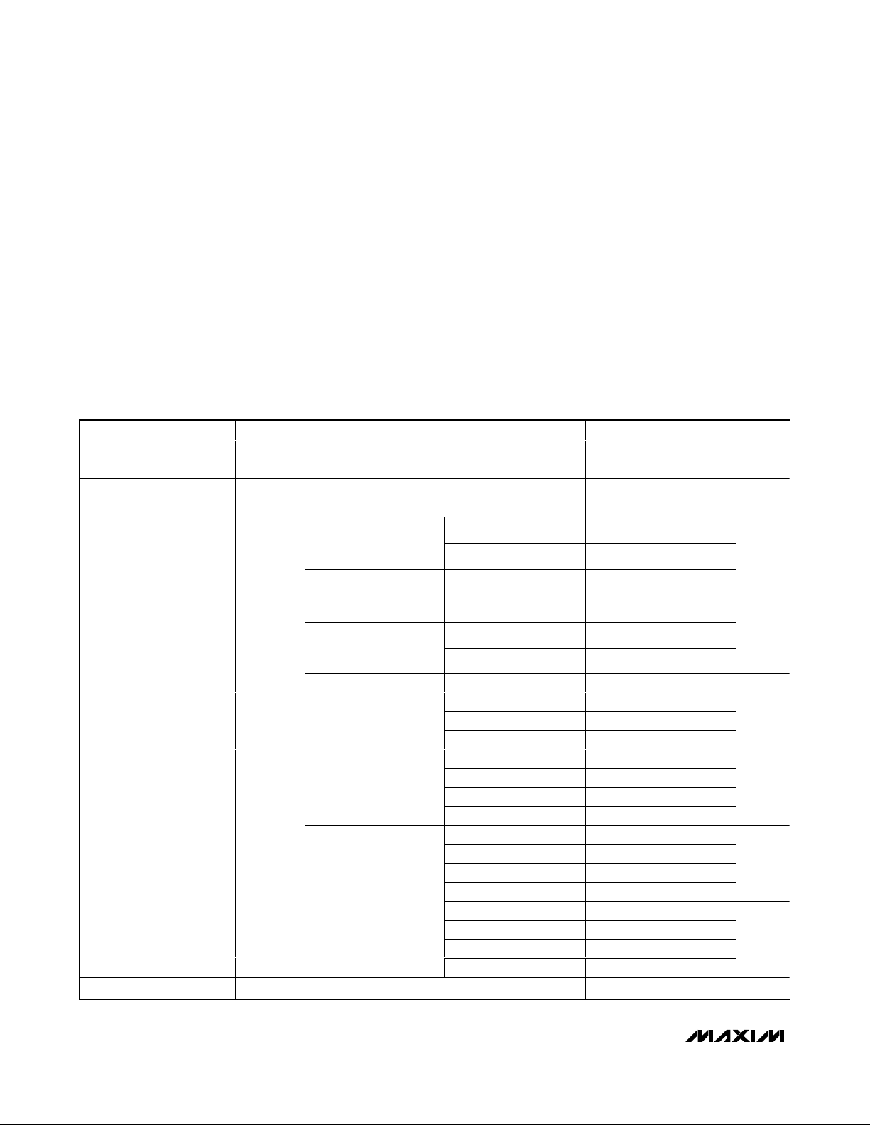
Ordering Information
19-3685; Rev 0; 5/05
For pricing, delivery, and ordering information, please contact Maxim/Dallas Direct! at
1-888-629-4642, or visit Maxim’s website at www.maxim-ic.com.
*0.2% BER, 4kbps Manchester-encoded data, 280kHz IF BW,
average RF power
**EP = Exposed paddle.
Pin Configuration, Typical Application Circuit, and
Functional Diagram appear at end of data sheet.
PART TEMP RANGE PIN-PACKAGE
MAX7032ATJ -40°C to +125°C 32 Thin QFN-EP** T3255-3
PKG
CODE
Page 2
MAX7032
Low-Cost, Crystal-Based, Programmable,
ASK/FSK Transceiver with Fractional-N PLL
2 _______________________________________________________________________________________
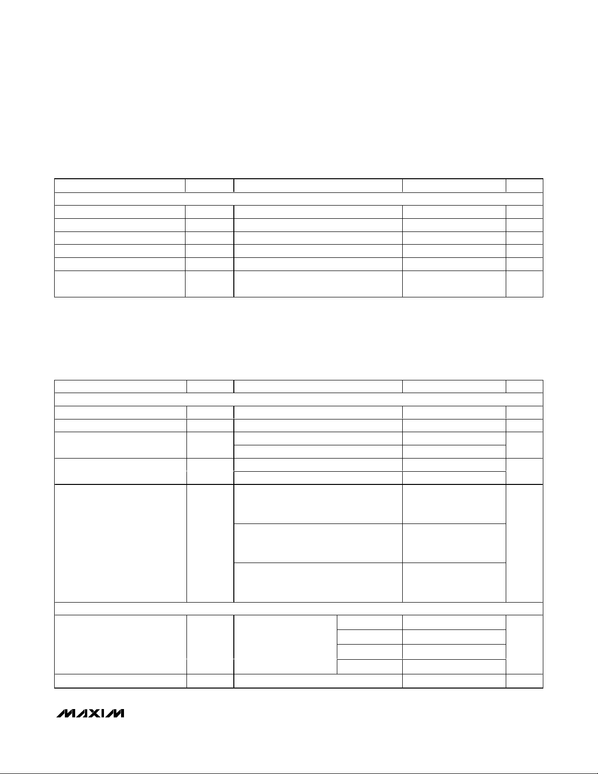
ABSOLUTE MAXIMUM RATINGS
Stresses beyond those listed under “Absolute Maximum Ratings” may cause permanent damage to the device. These are stress ratings only, and functional
operation of the device at these or any other conditions beyond those indicated in the operational sections of the specifications is not implied. Exposure to
absolute maximum rating conditions for extended periods may affect device reliability.
HVINto GND..........................................................-0.3V to +6.0V
PAV
DD
, AVDD, DVDDto GND ................................-0.3V to +4.0V
ENABLE, T/R, DATA, CS, DIO, SCLK, CLKOUT to
GND ......................................................-0.3V to (HV
IN
+ 0.3V)
All Other Pins to GND...............................-0.3V to (_V
DD
+ 0.3V)
Continuous Power Dissipation (T
A
= +70°C)
32-Pin Thin QFN (derate 21.3mW/°C above +70°C)....1702mW
Operating Temperature Range .........................-40°C to +125°C
Storage Temperature Range .............................-65°C to +150°C
Lead Temperature (soldering, 10s) .................................+300°C
DC ELECTRICAL CHARACTERISTICS
(Typical Application Circuit, 50Ω system impedance, AVDD= DVDD= P
AVDD
= HVIN= +2.1V to +3.6V, fRF= 300MHz to 450MHz, TA=
-40°C to +125°C, unless otherwise noted. Typical values are at AV
DD
= DVDD= PAV
DD
= HVIN= +2.7V, TA= +25°C, unless otherwise
noted.) (Note 1)
PARAMETER SYMBOL CONDITIONS MIN TYP MAX UNITS
Supply Voltage (3V Mode) V
Supply Voltage (5V Mode) HV
Supply Current I
Voltage Regulator V
DD
DD
REG
HVIN, PAVDD, AVDD, and DVDD connected to
power supply
PAVDD, AVDD, and DVDD unconnected from HVIN,
IN
but connected together
Transmit mode, PA off,
V
at 0% duty cycle
DATA
(ASK) (Note 2)
Transmit mode, V
at 50% duty cycle
(ASK) (Notes 3, 4)
Transmit mode, V
at 100% duty cycle
(FSK)
TA < +85°C,
typ at +25°C
(Note 4)
TA < +125°C
typ at +125°C
(Note 2)
HVIN = 5V, I
LOAD
DATA
DATA
= 15mA 3.0 V
fRF = 315MHz
= 434MHz
f
RF
fRF = 315MHz
= 434MHz
f
RF
fRF = 315MHz (Note 4)
f
= 434MHz (Note 2)
RF
Receiver (ASK 315MHz)
Receiver (ASK 434MHz) 6.4 8.3
Receiver (FSK 315MHz) 6.4 8.4
Receiver (FSK 434MHz) 6.7 8.7
DRX (3V mode) 23.4 77.3
DRX (5V mode) 67.2 94.4
Deep-sleep (3V mode) 0.8 8.8
Deep-sleep (5V mode) 2.4 10.9
Receiver (ASK 315MHz)
Receiver (ASK 434MHz) 6.7 8.4
Receiver (FSK 315MHz) 6.8 8.7
Receiver (FSK 434MHz) 7.0 8.8
DRX (3V mode) 33.5 103.0
DRX (5V mode) 82.3 116.1
Deep-sleep (3V mode) 8.0 34.2
Deep-sleep (5V mode) 14.9 39.3
2.1 2.7 3.6 V
4.5 5.0 5.5 V
3.5 5.4
4.3 6.7
7.6 12.3
8.4 13.6
11.6 19.1
12.4 20.4
6.1 7.9
6.4 8.2
mA
mA
µA
mA
µA
Page 3
MAX7032
Low-Cost, Crystal-Based, Programmable,
ASK/FSK Transceiver with Fractional-N PLL
_______________________________________________________________________________________ 3
DC ELECTRICAL CHARACTERISTICS (continued)
(Typical Application Circuit, 50Ω system impedance, AVDD= DVDD= P
AVDD
= HVIN= +2.1V to +3.6V, fRF= 300MHz to 450MHz, TA=
-40°C to +125°C, unless otherwise noted. Typical values are at AV
DD
= DVDD= PAV
DD
= HVIN= +2.7V, TA= +25°C, unless otherwise
noted.) (Note 1)
AC ELECTRICAL CHARACTERISTICS
(Typical Application Circuit, 50Ω system impedance, AVDD= DVDD= PAVDD= HVIN= +2.1V to +3.6V, fRF= 300MHz to 450MHz, TA=
-40°C to +125°C, unless otherwise noted. Typical values are at PAV
DD
= AVDD= DVDD= HVIN= +2.7V, TA= +25°C, unless otherwise
noted.) (Note 1)
DIGITAL I/O
Input High Threshold V
Input Low Threshold V
Pulldown Sink Current SCLK, ENABLE, T/R, DATA (HVIN = 5.5V) 20 µA
Pullup Source Current DIO, CS (HVIN = 5.5V) 20 µA
Output-Low Voltage V
Output-High Voltage V
PARAMETER SYMBOL CONDITIONS MIN TYP MAX UNITS
(Note 2) 0.9 x HV
IH
(Note 2) 0.1 x HV
IL
I
OL
OH
= 500µA 0.15 V
SINK
I
SOURCE
= 500µA
IN
HV
-
IN
0.26
V
IN
V
V
PARAMETER SYMBOL CONDITIONS MIN TYP MAX UNITS
GENERAL CHARACTERISTICS
Frequency Range 300 450 MHz
Maximum Input Level P
Transmit Efficiency 100% Duty
Cycle
Transmit Efficiency 50% Duty
Cycle
RFIN
fRF = 315MHz (Note 6) 32
= 434MHz (Note 6) 30
f
RF
fRF = 315MHz (Note 6) 24
= 434MHz (Note 6) 22
f
RF
ENABLE or T/R transition low to high,
transmitter frequency settled to within
50kHz of the desired carrier
0dBm
200
%
%
ENABLE or T/R transition low to high,
Power-On Time t
RECEIVER
Sensitivity
Image Rejection (Note 8) 46 dB
ON
transmitter frequency settled to within 5kHz
of the desired carrier
ENABLE transition low to high, or T/R
transition high to low receiver startup time
(Note 5)
0.2% BER, 4kbps
Manchester data rate,
280kHz IF BW, ±50kHz
FSK deviation,
average power
ASK (315MHz) -114
ASK (434MHz) -113
FSK (315MHz) -110
FSK (434MHz) -107
350
250
µs
dBm
Page 4
MAX7032
Low-Cost, Crystal-Based, Programmable,
ASK/FSK Transceiver with Fractional-N PLL
4 _______________________________________________________________________________________
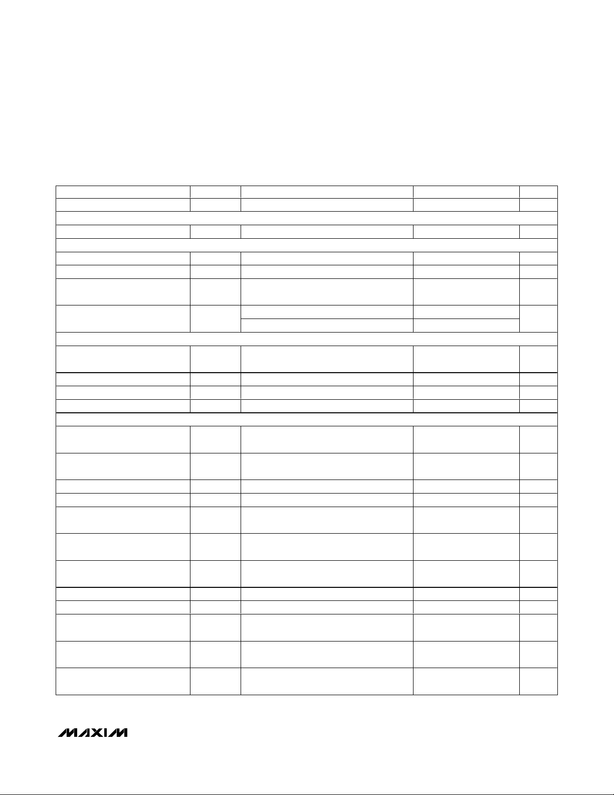
AC ELECTRICAL CHARACTERISTICS (continued)
(Typical Application Circuit, 50Ω system impedance, AVDD= DVDD= PAVDD= HVIN= +2.1V to +3.6V, fRF= 300MHz to 450MHz, TA=
-40°C to +125°C, unless otherwise noted. Typical values are at PAV
DD
= AVDD= DVDD= HVIN= +2.7V, TA= +25°C, unless otherwise
noted.) (Note 1)
PARAMETER SYMBOL CONDITIONS MIN TYP MAX UNITS
POWER AMPLIFIER
TA = +25°C (Note 4) 4.6 10.0 15.5
Output Power P
Modulation Depth 82 dB
Maximum Carrier Harmonics With output-matching network -40 dBc
Reference Spur -50 dBc
PHASE-LOCKED LOOP
Transmit VCO Gain K
Transmit PLL Phase Noise
Receive VCO Gain 340 MHz/V
Receive PLL Phase Noise
Loop Bandwidth
Minimum Transmit Frequency
Step
Reference Frequency Input Level 0.5 V
Programmable Divider Range In transmit mode (Note 4) 20 27
LOW-NOISE AMPLIFIER/MIXER (Note 9)
LNA Input Impedance Z
Voltage-Conversion Gain
Input-Referred 3rd-Order
Intercept Point
Mixer Output Impedance 330 Ω
LO Signal Feedthrough to
Antenna
RSSI
Input Impedance 330 Ω
Operating Frequency f
3dB Bandwidth 10 MHz
OUT
VCO
INLNA
IIP3
IF
TA = +125°C, AVDD = DVDD = HVIN =
= +2.1V (Note 2)
PAV
DD
TA = -40°C, AVDD = DVDD = HVIN =
= +3.6V (Note 4)
PAV
DD
10kHz offset, 200kHz loop BW -68
1MHz offset, 200kHz loop BW -98
10kHz offset, 500kHz loop BW -80
1MHz offset, 500kHz loop BW -90
Transmit PLL 200
Receive PLL 500
Normalized to
50Ω
High-gain state
Low-gain state
High-gain state -42
Low-gain state -6
3.9 6.7
13.1 15.8
340 MHz/V
f
/
XTAL
4096
fRF = 315MHz 1 - j4.7
f
= 434MHz 1 - j3.3
RF
fRF = 315MHz 50
= 434MHz 45
f
RF
fRF = 315MHz 13
= 434MHz 9
f
RF
-100 dBm
10.7 MHz
dBm
dBc/Hz
dBc/Hz
kHz
kHz
P-P
dB
dBm
Page 5
MAX7032
Low-Cost, Crystal-Based, Programmable,
ASK/FSK Transceiver with Fractional-N PLL
_______________________________________________________________________________________ 5
AC ELECTRICAL CHARACTERISTICS (continued)
(Typical Application Circuit, 50Ω system impedance, AVDD= DVDD= PAVDD= HVIN= +2.1V to +3.6V, fRF= 300MHz to 450MHz, TA=
-40°C to +125°C, unless otherwise noted. Typical values are at PAV
DD
= AVDD= DVDD= HVIN= +2.7V, TA= +25°C, unless otherwise
noted.) (Note 1)
Gain 15 mV/dB
FSK DEMODULATOR
Conversion Gain 2.0 mV/kHz
ANALOG BASEBAND
Maximum Data Filter Bandwidth 50 kHz
Maximum Data Slicer Bandwidth 100 kHz
Maximum Peak Detector
Bandwidth
Maximum Data Rate
CRYSTAL OSCILLATOR
Crystal Frequency f
Maximum Crystal Inductance 50 mH
Frequency Pulling by V
Crystal Load Capacitance (Note 7) 4.5 pF
SERIAL INTERFACE TIMING CHARACTERISTICS (see Figure 7)
Minimum SCLK Setup to Falling
Edge of CS
Minimum CS Falling Edge to
SCLK Rising-Edge Setup Time
Minimum CS Idle Time t
Minimum CS Period t
Maximum SCLK Falling Edge to
Data Valid Delay
Minimum Data Valid to SCLK
Rising-Edge Setup Time
Minimum Data Valid to SCLK
Rising-Edge Hold Time
Minimum SCLK High Pulse Width t
Minimum SCLK Low Pulse Width t
Minimum CS Rising Edge to
SCLK Rising-Edge Hold Time
Maximum CS Falling Edge to
Output Enable Time
Maximum CS Rising Edge to
Output Disable Time
PARAMETER SYMBOL CONDITIONS MIN TYP MAX UNITS
Manchester coded 33
NRZ 66
XTAL
DD
t
SC
t
CSS
CSI
CS
t
DO
t
DS
t
DH
CH
CL
t
CSH
t
DV
t
TR
50 kHz
(fRF - 10.7)
/ 24
2 ppm/V
30 ns
30 ns
125 ns
2.125 µs
80 ns
30 ns
30 ns
100 ns
100 ns
30 ns
25 ns
25 ns
kbps
MHz
Page 6
MAX7032
Low-Cost, Crystal-Based, Programmable,
ASK/FSK Transceiver with Fractional-N PLL
6 _______________________________________________________________________________________
AC ELECTRICAL CHARACTERISTICS (continued)
(Typical Application Circuit, 50Ω system impedance, AVDD= DVDD= PAVDD= HVIN= +2.1V to +3.6V, fRF= 300MHz to 450MHz, TA=
-40°C to +125°C, unless otherwise noted. Typical values are at PAV
DD
= AVDD= DVDD= HVIN= +2.7V, TA= +25°C, unless otherwise
noted.) (Note 1)
Note 1: Supply current, output power, and efficiency are greatly dependent on board layout and PAOUT match.
Note 2: 100% tested at T
A
= +125°C. Guaranteed by design and characterization overtemperature.
Note 3: 50% duty cycle at 10kHz ASK data (Manchester coded).
Note 4: Guaranteed by design and characterization. Not production tested.
Note 5: Time for final signal detection; does not include baseband filter settling.
Note 6: Efficiency = P
OUT
/ (VDDx IDD).
Note 7: Dependent on PC board trace capacitance.
Note 8: The oscillator register (0x05) is set to the nearest integer result of f
XTAL
/ 100kHz (see the Oscillator Frequency Register sec-
tion).
Note 9: Input impedance is measured at the LNAIN pin. Note that the impedance at 315MHz includes the 12nH inductive degenera-
tion from the LNA source to ground. The impedance at 434MHz includes a 10nH inductive degeneration connected from the
LNA source to ground. The equivalent input circuit is approximately 50Ω in series with ~ 2.2pF. The voltage conversion is
measured with the LNA input matching inductor, the degeneration inductor, and the LNA/mixer tank in place, and does not
include the IF filter insertion loss.
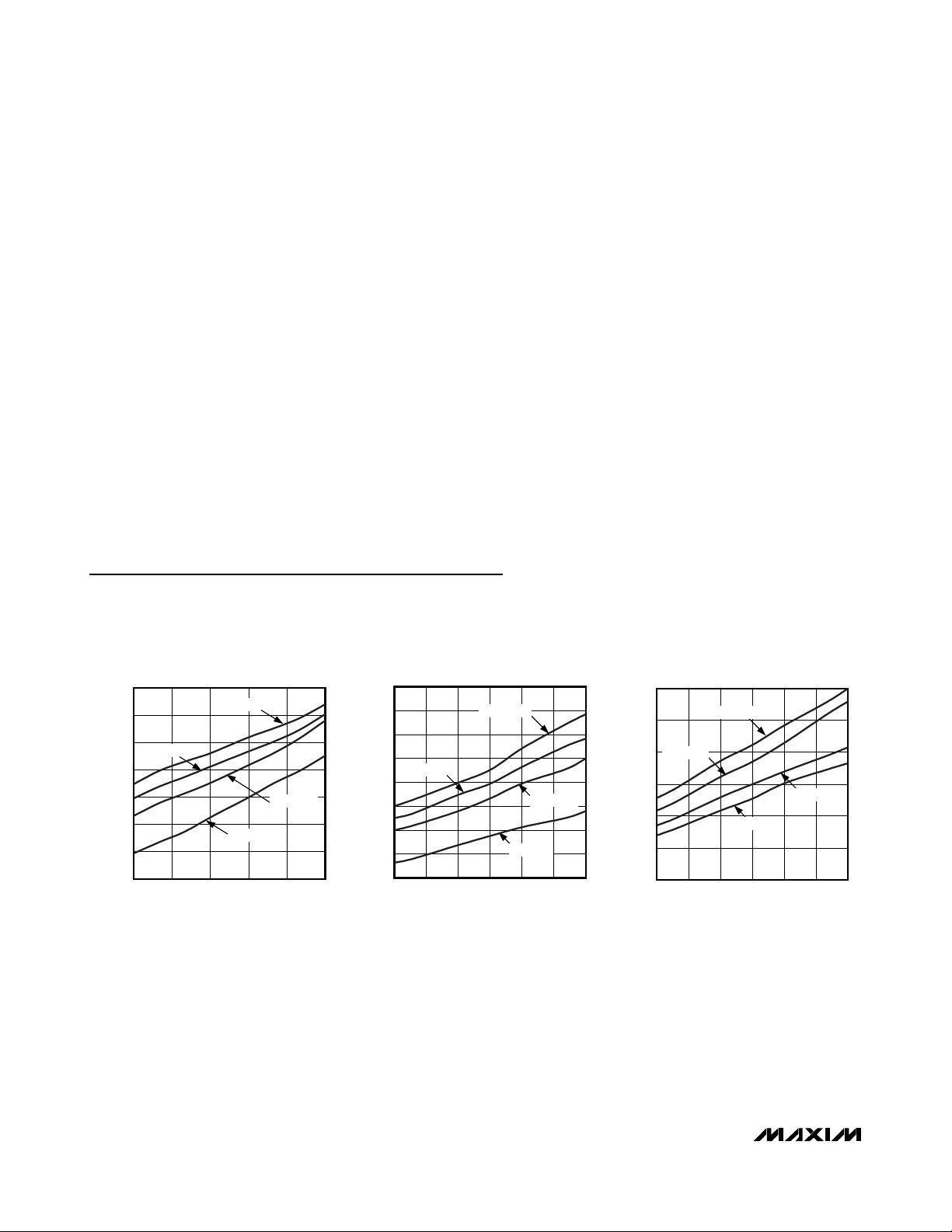
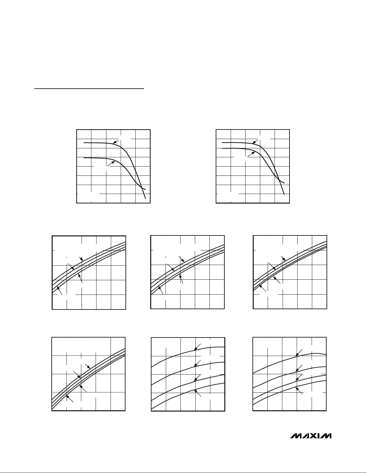
Typical Operating Characteristics
(Typical Operating Circuit, PAVDD= AVDD= DVDD= HVIN= +3.0V, fRF= 433.92MHz, TA= +25°C, IF BW = 280kHz, data rate =
4kbps Manchester encoded, frequency deviation = ±50kHz, BER = 0.2% average RF power, unless otherwise noted.)
SUPPLY CURRENT vs. SUPPLY VOLTAGE
(ASK MODE)
MAX7032 toc01
SUPPLY VOLTAGE (V)
SUPPLY CURRENT (mA)
3.33.02.72.4
5.8
6.0
6.2
6.4
6.6
6.8
7.0
5.6
2.1 3.6
TA = +85°C
TA = +125°C
TA = +25°C
TA = -40°C
SUPPLY CURRENT vs. RF FREQUENCY
(ASK MODE)
MAX7032 toc02a
RF FREQUENCY (MHz)
SUPPLY CURRENT (mA)
425400325 350 375
6.1
6.2
6.3
6.4
6.5
6.6
6.7
6.8
6.0
300 450
TA = +85°C
TA = +125°C
TA = +25°C
TA = -40°C
SUPPLY CURRENT vs. RF FREQUENCY
(FSK MODE)
MAX7032 toc02b
RF FREQUENCY (MHz)
SUPPLY CURRENT (mA)
425400325 350 375
6.5
6.6
6.7
6.8
6.9
7.0
6.4
300 450
TA = +85°C
TA = +125°C
TA = +25°C
TA = -40°C
RECEIVER
Page 7
MAX7032
Low-Cost, Crystal-Based, Programmable,
ASK/FSK Transceiver with Fractional-N PLL
_______________________________________________________________________________________ 7
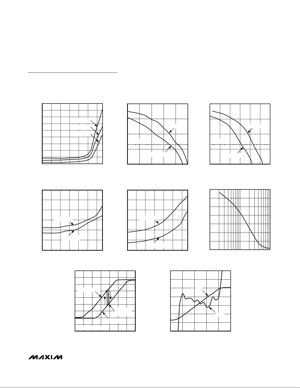
Typical Operating Characteristics (continued)
(Typical Operating Circuit, PAVDD= AVDD= DVDD= HVIN= +3.0V, fRF= 433.92MHz, TA= +25°C, IF BW = 280kHz, data rate =
4kbps Manchester encoded, frequency deviation = ±50kHz, BER = 0.2% average RF power, unless otherwise noted.)
RECEIVER
DEEP-SLEEP CURRENT vs. TEMPERATURE
18
16
14
12
10
8
6
DEEP-SLEEP CURRENT (µA)
4
2
0
-40
TEMPERATURE (°C)
VCC = +3.6V
VCC = +3.0V
VCC = +2.1V
SENSITIVITY vs. TEMPERATURE
(ASK DATA)
-102
-105
-108
-111
SENSITIVITY (dBm)
-114
-117
-120
fRF = 434MHz
fRF = 315MHz
TEMPERATURE (°C)
RSSI vs. RF INPUT POWER
1.8
1.6
1.4
HIGH-GAIN MODE
1.2
1.0
RSSI (V)
0.8
0.6
0.4
0.2
AGC HYSTERESIS: 3dB
0
-130 10
MAX7032 toc03
1108535 60-10-15
MAX7032 toc06
11085603510-15-40
AGC SWITCH
POINT
LOW-GAIN MODE
RF INPUT POWER (dBm)
vs. AVERAGE INPUT POWER (ASK DATA)
BIT-ERROR RATE
100
10
fRF = 434MHz
1
BIT-ERROR RATE (%)
0.2% BER
0.1
fRF = 315MHz
0.01
-121 -111
AVERAGE INPUT POWER (dBm)
SENSITIVITY vs. TEMPERATURE
(FSK DATA)
-100
-102
-104
-106
SENSITIVITY (dBm)
-108
-110
-112
fRF = 434MHz
fRF = 315MHz
TEMPERATURE (°C)
RSSI AND DELTA vs. IF INPUT POWER
2.1
MAX7032 toc09
-10-30-70 -50-90-110
1.8
1.5
1.2
RSSI (V)
0.9
0.6
0.3
0
-90 10
-113-115-117-119
11085603510-15-40
vs. AVERAGE INPUT POWER (FSK DATA)
100
MAX7030 toc04
10
1
BIT-ERROR RATE (%)
0.1
0.01
-116 -104
SENSITIVITY vs. FREQUENCY DEVIATION
-94
-96
MAX7032 toc07
-98
-100
-102
SENSITIVITY (dBm)
-104
-106
-108
1 100
RSSI
IF INPUT POWER (dBm)
BIT-ERROR RATE
0.2% BER
fRF = 315MHz
AVERAGE INPUT POWER (dBm)
(FSK DATA)
10
FREQUENCY DEVIATION (kHz)
MAX7032 toc10
DELTA
-10-30-50-70
3.5
2.5
1.5
0.5
-0.5
-1.5
-2.5
-3.5
fRF = 434MHz
-108 -106-110-112-114
DELTA (%)
MAX7032 toc05
MAX7032 toc08
Page 8
MAX7032
Low-Cost, Crystal-Based, Programmable,
ASK/FSK Transceiver with Fractional-N PLL
8 _______________________________________________________________________________________
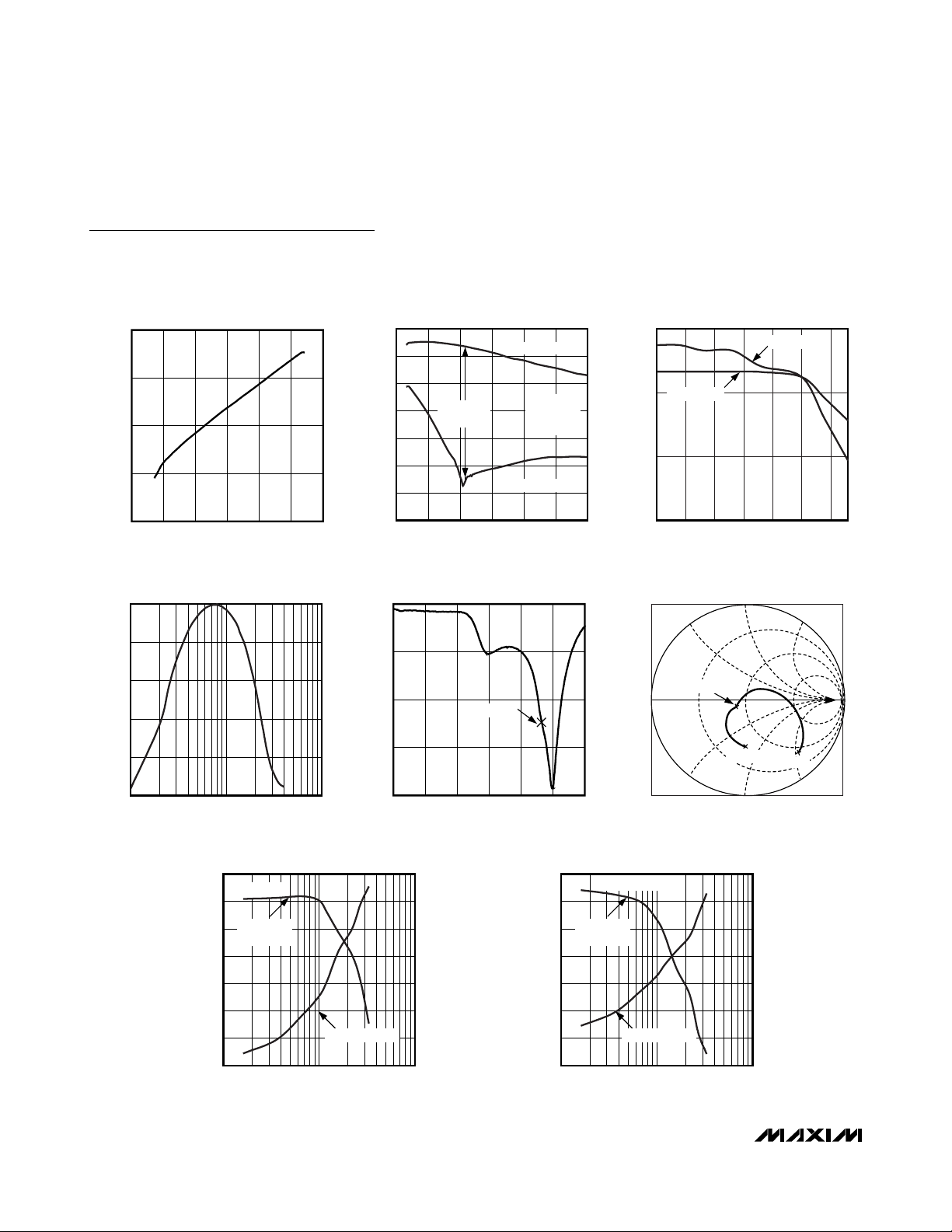
Typical Operating Characteristics (continued)
(Typical Operating Circuit, PAVDD= AVDD= DVDD= HVIN= +3.0V, fRF= 433.92MHz, TA= +25°C, IF BW = 280kHz, data rate =
4kbps Manchester encoded, frequency deviation = ±50kHz, BER = 0.2% average RF power, unless otherwise noted.)
RECEIVER
FSK DEMODULATOR OUTPUT
vs. IF FREQUENCY
1.6
1.2
0.8
0.4
FSK DEMODULATOR OUTPUT (V)
MAX7032 toc11
SYSTEM GAIN (dBm)
50
40
30
20
10
0
-10
SYSTEM GAIN vs. IF FREQUENCY
UPPER SIDEBAND
48dB IMAGE
REJECTION
FROM RFIN
TO MIXOUT
= 434MHz
f
RF
LOWER SIDEBAND
48
MAX7032 toc12
46
44
IMAGE REJECTION (dB)
IMAGE REJECTION vs. TEMPERATURE
fRF = 434MHz
fRF = 315MHz
MAX7032 toc13
0
10.4 11.0
IF FREQUENCY (MHz)
NORMALIZED IF GAIN vs. IF FREQUENCY
0
-4
-8
-12
NORMALIZED IF GAIN (dB)
-16
-20
1 100
10
IF FREQUENCY (MHz)
vs. INDUCTIVE DEGENERATION
90
fRF = 315MHz
80
IMAGINARY
70
IMPEDANCE
60
10.910.810.710.610.5
MAX7032 toc14
INPUT IMPEDANCE
-20
030
IF FREQUENCY (MHz)
252015105
S11 vs. RF FREQUENCY
0
-6
-12
S11 (dB)
-18
-24
200 500
433.92MHz
450400350300250
RF FREQUENCY (MHz)
42
S11 SMITH PLOT OF RFIN
MAX7032 toc15
434MHz
INPUT IMPEDANCE
MAX7032 toc17
-220
-230
-240
-250
vs. INDUCTIVE DEGENERATION
90
80
70
60
fRF = 434MHz
IMAGINARY
IMPEDANCE
TEMPERATURE (
400MHz
MAX7032 toc18
-150
-160
-170
-180
11085603510-15-40
°C)
MAX7032 toc16
500MHz
50
REAL IMPEDANCE (Ω)
40
30
20
1 100
INDUCTIVE DEGENERATION (nH)
REAL IMPEDANCE
10
-260
-270
-280
-290
IMAGINARY IMPEDANCE (Ω)
50
REAL IMPEDANCE (Ω)
40
30
20
1 100
REAL IMPEDANCE
10
INDUCTIVE DEGENERATION (nH)
-190
-200
-210
-220
IMAGINARY IMPEDANCE (Ω)
Page 9
MAX7032
Low-Cost, Crystal-Based, Programmable,
ASK/FSK Transceiver with Fractional-N PLL
_______________________________________________________________________________________ 9
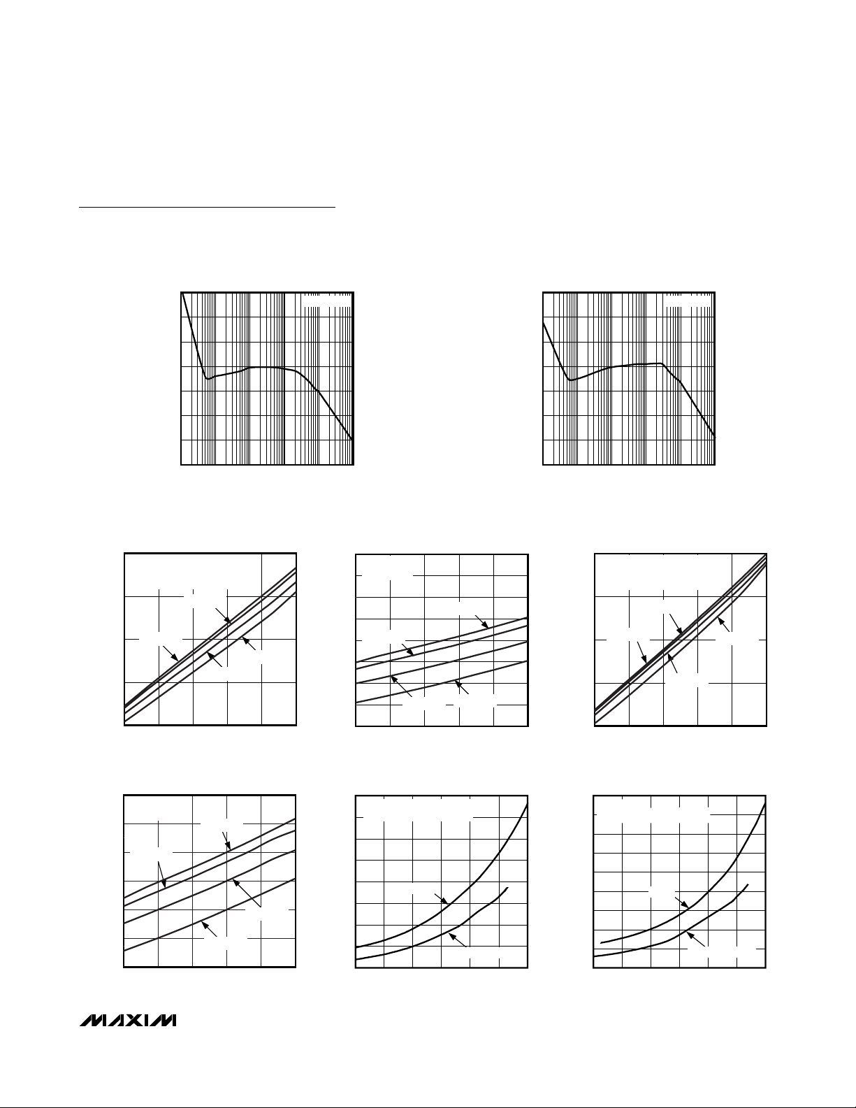
Typical Operating Characteristics (continued)
(Typical Operating Circuit, PAVDD= AVDD= DVDD= HVIN= +3.0V, fRF= 433.92MHz, TA= +25°C, IF BW = 280kHz, data rate =
4kbps Manchester encoded, frequency deviation = ±50kHz, BER = 0.2% average RF power, unless otherwise noted.)
RECEIVER
TRANSMITTER
PHASE NOISE vs. OFFSET FREQUENCY
-50
-60
-70
-80
-90
PHASE NOISE (dBc/Hz)
-100
-110
-120
100 10M
OFFSET FREQUENCY (Hz)
fRF = 315MHz
MAX7032 toc19
1M100k10k1k
PHASE NOISE vs. OFFSET FREQUENCY
-50
-60
-70
-80
-90
PHASE NOISE (dBc/Hz)
-100
-110
-120
100 10M
OFFSET FREQUENCY (Hz)
fRF = 434MHz
MAX7032 toc20
1M100k10k1k
SUPPLY CURRENT vs. SUPPLY VOLTAGE
16
fRF = 315MHz
PA ON
WITHOUT ENVELOPE SHAPING
14
TA = +125°C
12
SUPPLY CURRENT (mA)
10
8
2.1 3.6
TA = +85°C
TA = +25°C
SUPPLY VOLTAGE (V)
SUPPLY CURRENT
vs. SUPPLY VOLTAGE
6.0
fRF = 434MHz
PA OFF
5.5
5.0
TA = +85°C
4.5
4.0
SUPPLY CURRENT (mA)
3.5
3.0
TA = +125°C
TA = -40°C
SUPPLY VOLTAGE (V)
TA = -40°C
3.33.02.72.4
TA = +25°C
3.33.02.72.42.1 3.6
6.0
5.5
MAX7032 toc21
5.0
4.5
4.0
3.5
SUPPLY CURRENT (mA)
3.0
2.5
2.0
12
11
MAX7032 toc24
10
9
8
7
SUPPLY CURRENT (mA)
6
5
4
-14 10
SUPPLY CURRENT vs. OUTPUT POWER
SUPPLY CURRENT
vs. SUPPLY VOLTAGE
fRF = 315MHz
PA OFF
TA = +125°C
TA = +85°C
TA = +25°C
SUPPLY VOLTAGE (V)
fRF = 315MHz
ENVELOPE SHAPING ENABLED
PA ON
50% DUTY CYCLE
AVERAGE OUTPUT POWER (dBm)
TA = -40°C
3.33.02.72.42.1 3.6
62-10 -6 -2
17
MAX7032 toc22
MAX7032 toc25
15
13
SUPPLY CURRENT (mA)
11
14
13
12
11
10
SUPPLY CURRENT (mA)
SUPPLY CURRENT vs. SUPPLY VOLTAGE
fRF = 434MHz
PA ON
WITHOUT ENVELOPE SHAPING
TA = +85°C
TA = +125°C
TA = +25°C
9
2.1 3.6
SUPPLY VOLTAGE (V)
TA = -40°C
3.33.02.72.4
SUPPLY CURRENT vs. OUTPUT POWER
fRF = 434MHz
ENVELOPE SHAPING ENABLED
9
8
7
6
5
-14 10
PA ON
50% DUTY CYCLE
62-2-6-10
AVERAGE OUTPUT POWER (dBm)
MAX7032 toc23
MAX7032 toc26
Page 10
MAX7032
Low-Cost, Crystal-Based, Programmable,
ASK/FSK Transceiver with Fractional-N PLL
10 ______________________________________________________________________________________
Typical Operating Characteristics (continued)
(Typical Operating Circuit, PAVDD= AVDD= DVDD= HVIN= +3.0V, fRF= 433.92MHz, TA= +25°C, IF BW = 280kHz, data rate =
4kbps Manchester encoded, frequency deviation = ±50kHz, BER = 0.2% average RF power, unless otherwise noted.)
TRANSMITTER
SUPPLY CURRENT AND OUTPUT POWER
18
16
14
12
10
8
SUPPLY CURRENT (mA)
6
4
2
0.1 10k
OUTPUT POWER vs. SUPPLY VOLTAGE
14
fRF = 315MHz
PA ON
ENVELOPE SHAPING DISABLED
12
10
8
OUTPUT POWER (dBm)
6
TA = -40°C
TA = +25°C
TA = +125°C
TA = +85°C
vs. EXTERNAL RESISTOR
CURRENT
fRF = 315MHz
PA ON
EXTERNAL RESISTOR (Ω)
POWER
MAX7032 toc27-1
1k1001 10
14
MAX7032 28-1
12
10
8
OUTPUT POWER (dBm)
6
16
12
8
4
0
-4
OUTPUT POWER (dBm)
-8
-12
-16
SUPPLY CURRENT AND OUTPUT POWER
18
16
14
12
10
8
SUPPLY CURRENT (mA)
6
4
fRF = 434MHz
PA ON
2
0.1 10k
OUTPUT POWER vs. SUPPLY VOLTAGE
fRF = 315MHz
PA ON
ENVELOPE SHAPING ENABLED
TA = -40°C
TA = +25°C
TA = +125°C
TA = +85°C
vs. EXTERNAL RESISTOR
POWER
CURENT
EXTERNAL RESISTOR (Ω)
OUTPUT POWER vs. SUPPLY VOLTAGE
14
fRF = 434MHz
PA ON
MAX7032 28-2
ENVELOPE SHAPING DISABLED
12
10
8
OUTPUT POWER (dBm)
6
TA = -40°C
TA = +25°C
TA = +85°C
MAX7032 toc27-2
1k1001 10
TA = +125°C
16
12
8
4
0
-4
OUTPUT POWER (dBm)
-8
-12
-16
MAX7032 29-1
4
2.1 3.6
SUPPLY VOLTAGE (V)
OUTPUT POWER vs. SUPPLY VOLTAGE
14
fRF = 434MHz
PA ON
ENVELOPE SHAPING ENABLED
12
10
OUTPUT POWER (dBm)
8
6
2.1 3.6
TA = -40°C
TA = +25°C
TA = +125°C
TA = +85°C
SUPPLY VOLTAGE (V)
4
3.33.02.72.4
2.1 3.6
SUPPLY VOLTAGE (V)
3.33.02.72.4
EFFICIENCY vs. SUPPLY VOLTAGE
40
fRF = 315MHz
MAX7032 29-2
3.33.02.72.4
PA ON
35
30
EFFICIENCY (%)
25
20
2.1 3.6
SUPPLY VOLTAGE (V)
TA = -40°C
MAX7032 toc30
TA = +25°C
TA = +85°C
TA = +125°C
3.33.02.72.4
4
2.1 3.6
SUPPLY VOLTAGE (V)
EFFICIENCY vs. SUPPLY VOLTAGE
40
fRF = 434MHz
PA ON
35
30
EFFICIENCY (%)
25
20
2.1 3.6
SUPPLY VOLTAGE (V)
3.33.02.72.4
TA = -40°C
TA = +25°C
TA = +85°C
TA = +125°C
3.33.02.72.4
MAX7032 toc31
Page 11

MAX7032
Low-Cost, Crystal-Based, Programmable,
ASK/FSK Transceiver with Fractional-N PLL
______________________________________________________________________________________ 11
Typical Operating Characteristics (continued)
(Typical Operating Circuit, PAVDD= AVDD= DVDD= HVIN= +3.0V, fRF= 433.92MHz, TA= +25°C, IF BW = 280kHz, data rate =
4kbps Manchester encoded, frequency deviation = ±50kHz, BER = 0.2% average RF power, unless otherwise noted.)
TRANSMITTER
EFFICIENCY vs. SUPPLY VOLTAGE
30
fRF = 315MHz
50% DUTY CYCLE
25
20
EFFICIENCY (%)
15
10
2.1 3.6
SUPPLY VOLTAGE (V)
TA = -40°C
TA = +85°C
vs. OFFSET FREQUENCY
-40
fRF = 434MHz
-50
-60
-70
-80
-90
-100
PHASE NOISE (dBc/Hz)
-110
-120
-130
-140
100 10M
OFFSET FREQUENCY (Hz)
MAX7032 toc32
TA = +25°C
TA = +125°C
3.33.02.72.4
PHASE NOISE
1M100k10k1k
EFFICIENCY vs. SUPPLY VOLTAGE
30
fRF = 434MHz
50% DUTY CYCLE
25
EFFICIENCY (%)
20
15
2.1 3.6
SUPPLY VOLTAGE (V)
MAX7032 toc35
TA = -40°C
TA = +25°C
TA = +125°C
-40
-50
MAX7032 toc33
-60
-70
-80
-90
-100
PHASE NOISE (dBc/Hz)
TA = +85°C
3.33.02.72.4
-110
-120
-130
-140
REFERENCE SPUR MAGNITUDE
vs. SUPPLY VOLTAGE
-40
-45
-50
-55
-60
-65
REFERENCE SPUR MAGNITUDE (dBc)
-70
2.1 3.6
PHASE NOISE vs. OFFSET FREQUENCY
fRF = 315MHz
100 10M
OFFSET FREQUENCY (Hz)
433.92MHz
315MHz
3.33.02.72.4
SUPPLY VOLTAGE (V)
1M100k10k1k
MAX7032 toc36
MAX7032 toc34
FREQUENCY STABILITY
vs. SUPPLY VOLTAGE
10
8
6
4
2
0
-2
-4
FREQUENCY STABILITY (ppm)
-6
-8
-10
2.1 3.6
fRF = 315MHz
fRF = 434MHz
SUPPLY VOLTAGE (V)
-56
MAX7032 toc37
3.33.02.72.4
-58
-60
-62
-64
CLKOUT SPUR MAGNITUDE (dBc)
-66
CLKOUT SPUR MAGNITUDE
vs. SUPPLY VOLTAGE
fRF = 434MHz
CLKOUT SPUR = f
10pF LOAD CAPACITANCE
f
= f
CLKOUT
2.1 3.6
± f
RF
CLKOUT
/ 8
XTAL
f
= f
CLKOUT
XTAL
SUPPLY VOLTAGE (V)
f
CLKOUT
/ 4
= f
/ 2
XTAL
3.33.02.72.4
MAX7032 toc38
Page 12

MAX7032
Low-Cost, Crystal-Based, Programmable,
ASK/FSK Transceiver with Fractional-N PLL
12 ______________________________________________________________________________________
Pin Description
PIN NAME FUNCTION
1 PAV
2 ROUT
Power-Amplifier Supply Voltage. Bypass to GND with 0.01µF and 220pF capacitors placed as close
DD
to the pin as possible.
Envelope-Shaping Output. ROUT controls the power-amplifier envelope’s rise and fall times. Connect
ROUT to the PA pullup inductor or optional power-adjust resistor. Bypass the inductor to GND as
close to the inductor as possible with 680pF and 220pF capacitors as shown in the Typical
Application Circuit.
3 TX/RX1
4 TX/RX2 Transmit/Receive Switch Pole. Typically connected to ground. See the Typical Application Circuit.
5 PAOUT
6AV
7 LNAIN Low-Noise Amplifier Input. Must be AC-coupled.
8 LNASRC
9 LNAOUT
10 MIXIN+ Noninverting Mixer Input. Must be AC-coupled to the LNA output.
11 MIXIN- Inverting Mixer Input. Bypass to AVDD with a capacitor as close to LNA LC tank filter as possible.
12 MIXOUT 330Ω Mixer Output. Connect to the input of the 10.7MHz filter.
13 IFIN- Inverting 330Ω IF Limiter Amplifier Input. Bypass to GND with a capacitor.
14 IFIN+ Noninverting 330Ω IF Limiter Amplifier Input. Connect to the output of the 10.7MHz IF filter.
15 PDMIN Minimum-Level Peak Detector for Demodulator Output
16 PDMAX Maximum-Level Peak Detector for Demodulator Output
17 DS- Inverting Data Slicer Input
18 DS+ Noninverting Data Slicer Input
19 OP+ Noninverting Op Amp Input for the Sallen-Key Data Filter
20 DF Data Filter Feedback Node. Input for the feedback of the Sallen-Key data filter.
21 RSSI Buffered Received-Signal-Strength Indicator Output
22 T/R
DD
Transmit/Receive Switch Throw. Drive T/R high to short TX/RX1 to TX/RX2. Drive T/R low to disconnect
TX/RX1 from TX/RX2. Functionally identical to TX/RX2.
Power-Amplifier Output. Requires a pullup inductor to the supply voltage (or ROUT if envelope
shaping is desired), which may be part of the output-matching network to an antenna.
Analog Power-Supply Voltage. AVDD is connected to an on-chip +3.0V regulator in 5V operation.
Bypass AV
Low-Noise Amplifier Source for External Inductive Degeneration. Connect an inductor to GND to set
the LNA input impedance.
Low-Noise Amplifier Output. Must be tied to AV
MIXIN+.
Transmit/ Receive. Drive high to put the device in transmit mode. Drive low or leave unconnected to
put the device in receive mode. It is internally pulled down. This function is also controlled by a
configuration register.
to GND with 0.1µF and 220pF capacitors placed as close to the pin as possible.
DD
through a parallel LC tank filter. AC-couple to
DD
23 ENABLE
24 DATA Receiver Data Output/Transmitter Data Input
25 CLKOUT Divided Crystal Clock Buffered Output
26 DV
DD
Enable. Drive high for normal operation. Drive low or leave unconnected to put the device into
shutdown mode.
Digital Power-Supply Voltage. Bypass to GND with 0.01µF and 220pF capacitors placed as close to
the pin as possible.
Page 13

Detailed Description
The MAX7032 300MHz to 450MHz CMOS transceiver
and a few external components provide a complete
transmit and receive chain from the antenna to the digital data interface. This device is designed for transmitting and receiving ASK and FSK data. All transmit
frequencies are generated by a fractional-N-based synthesizer, allowing for very fine frequency steps in increments of f
XTAL
/ 4096. The receive LO is generated by
a traditional integer-N-based synthesizer. Depending
on component selection, data rates as high as 33kbps
(Manchester encoded) or 66kbps (NRZ encoded) can
be achieved.
Receiver
Low-Noise Amplifier (LNA)
The LNA is a cascode amplifier with off-chip inductive
degeneration that achieves approximately 30dB of voltage gain that is dependent on both the antenna matching network at the LNA input, and the LC tank network
between the LNA output and the mixer inputs.
The off-chip inductive degeneration is achieved by
connecting an inductor from LNASRC to AGND. This
inductor sets the real part of the input impedance at
LNAIN, allowing for a more flexible match for low-input
impedance such as a PC board trace antenna. A nominal value for this inductor with a 50Ω input impedance
is 12nH at 315MHz and 10nH at 434MHz, but the
inductance is affected by PC board trace length.
LNASRC can be shorted to ground to increase sensitivity by approximately 1dB, but the input match must
then be reoptimized.
The LC tank filter connected to LNAOUT consists of L5
and C9 (see the Typical Application Circuit). Select L5
and C9 to resonate at the desired RF input frequency.
The resonant frequency is given by:
where L
TOTAL
= L5 + L
PARASITICS
and C
TOTAL
= C9 +
C
PARASITICS
.
L
PARASITICS
and C
PARASITICS
include inductance and
capacitance of the PC board traces, package pins,
mixer input impedance, LNA output impedance, etc.
These parasitics at high frequencies cannot be
ignored, and can have a dramatic effect on the tank filter center frequency. Lab experimentation must be
done to optimize the center frequency of the tank. The
total parasitic capacitance is generally between 5pF
and 7pF.
Automatic Gain Control (AGC)
When the AGC is enabled, it monitors the RSSI output.
When the RSSI output reaches 1.28V, which corresponds to an RF input level of approximately -55dBm,
the AGC switches on the LNA gain-reduction attenuator. The attenuator reduces the LNA gain by 36dB,
thereby reducing the RSSI output by about 540mV to
740mV. The LNA resumes high-gain mode when the
RSSI output level drops back below 680mV (approximately -59dBm at the RF input) for a programmable
interval called the AGC dwell time. The AGC has a hysteresis of approximately 4dB. With the AGC function,
the RSSI dynamic range is increased, allowing the
MAX7032 to reliably produce an ASK output for RF
input levels up to 0dBm with a modulation depth of
18dB. AGC is not required and can be disabled in
either ASK or FSK mode. AGC is not necessary for FSK
mode because large received signal levels do not
affect FSK performance.
MAX7032
Low-Cost, Crystal-Based, Programmable,
ASK/FSK Transceiver with Fractional-N PLL
______________________________________________________________________________________ 13
Pin Description (continued)
PIN NAME FUNCTION
High-Voltage Supply Input. For 3V operation, connect HVIN to PAVDD, AVDD, and DVDD. For 5V
27 HV
28 CS Serial Interface Active-Low Chip Select
29 DIO Serial Interface Serial Data Input/Output
30 SCLK Serial Interface Clock Input
31 XTAL1 Crystal Input 1. Bypass to GND if XTAL2 is driven by an AC-coupled external reference.
32 XTAL2 Crystal Input 2. XTAL2 can be driven from an AC-coupled external reference.
EP GND Exposed Paddle. Solder evenly to the board’s ground plane for proper operation.
operation, tie only HV
IN
close to the pin as possible.
to 5V. Bypass HVIN to GND with 0.01µF and 220pF capacitors placed as
IN
f
=
2π
1
LC
×
TOTAL TOTAL
Page 14

Mixer
A unique feature of the MAX7032 is the integrated
image rejection of the mixer. This eliminates the need
for a costly front-end SAW filter for many applications.
The advantage of not using a SAW filter is increased
sensitivity, simplified antenna matching, less board
space, and lower cost.
The mixer cell is a pair of double-balanced mixers that
perform an IQ downconversion of the RF input to the
10.7MHz intermediate frequency (IF) with low-side
injection (i.e., f
LO
= fRF- fIF). The image-rejection circuit
then combines these signals to achieve a typical 46dB
of image rejection over the full temperature range. Lowside injection is required as high-side injection is not
possible due to the on-chip image rejection. The IF output is driven by a source follower, biased to create a
driving impedance of 330Ω to interface with an off-chip
330Ω ceramic IF filter. The voltage-conversion gain driving a 330Ω load is approximately 20dB. Note that the
MIXIN+ and MIXIN- inputs are functionally identical.
Integer-N Phase-Locked Loop (PLL)
The MAX7032 utilizes a fixed integer-N PLL to generate
the receive LO. All PLL components, including the loop filter, VCO, charge pump, asynchronous 24x divider, and
phase-frequency detector are integrated on-chip. The
loop bandwidth is approximately 500kHz. The relationship
between RF, IF, and reference frequencies is given by:
f
REF
= (f
RF
– fIF) / 24
Intermediate Frequency (IF)
The IF section presents a differential 330Ω load to provide matching for the off-chip ceramic filter. The internal six AC-coupled limiting amplifiers produce an
overall gain of approximately 65dB, with a bandpass filter type response centered near the 10.7MHz IF frequency with a 3dB bandwidth of approximately 10MHz.
For ASK data, the RSSI circuit demodulates the IF to
baseband by producing a DC output proportional to
the log of the IF signal level with a slope of approximately 15mV/dB. For FSK, the limiter output is fed into a
PLL to demodulate the IF. The FSK demodulation slope
is approximately 2.0mV/kHz.
FSK Demodulator
The FSK demodulator uses an integrated 10.7MHz PLL
that tracks the input RF modulation and converts the frequency deviation into a voltage difference. The PLL is
illustrated in Figure 1. The input to the PLL comes from
the output of the IF limiting amplifiers. The PLL control
voltage responds to changes in the frequency of the
input signal with a nominal gain of 2.0mV/kHz. For example, an FSK peak-to-peak deviation of 50kHz generates
a 100mV
P-P
signal on the control line. This control volt-
age is then filtered and sliced by the baseband circuitry.
The FSK demodulator PLL requires calibration to overcome variations in process, voltage, and temperature.
For more information on calibrating the FSK demodulator, see the Calibration section. The maximum calibration time is 150µs. In discontinuous receive (DRX)
mode, the FSK demodulator calibration occurs automatically just after the IC exits sleep mode.
Data Filter
The data filter for the demodulated data is implemented
as a 2nd-order lowpass Sallen-Key filter. The pole locations are set by the combination of two on-chip resistors
and two external capacitors. Adjusting the value of the
external capacitors changes the corner frequency to
optimize for different data rates. The corner frequency in
kHz should be set to approximately 3 times the fastest
expected Manchester data rate in kbps from the transmitter (1.5 times the fastest expected NRZ data rate) for
ASK. For FSK, the corner frequency should be set to
approximately 2 times the fastest expected Manchester
data rate in kbps from the transmitter (1 times the fastest
expected NRZ data rate). Keeping the corner frequency
near the data rate rejects any noise at higher frequencies, resulting in an increase in receiver sensitivity.
Table 1 lists coefficients to calculate CF1 and CF2.
Table 1. Coefficients to Calculate CF1
and CF2
MAX7032
Low-Cost, Crystal-Based, Programmable,
ASK/FSK Transceiver with Fractional-N PLL
14 ______________________________________________________________________________________
Figure 1. FSK Demodulator PLL Block Diagram
IF
LIMITING
AMPS
FILTER TYPE a b
Butterworth
(Q = 0.707)
Bessel
(Q = 0.577)
PHASE
DETECTOR
CHARGE
PUMP
1.414 1.000
1.3617 0.618
LOOP
FILTER
TO FSK BASEBAND FILTER
AND DATA SLICER
10.7MHz VCO
2.0mV/kHz
Page 15

MAX7032
Low-Cost, Crystal-Based, Programmable,
ASK/FSK Transceiver with Fractional-N PLL
______________________________________________________________________________________ 15
The configuration shown in Figure 2 can create a
Butterworth or Bessel response. The Butterworth filter
offers a very flat amplitude response in the passband
and a rolloff rate of 40dB/decade for the two-pole filter.
The Bessel filter has a linear phase response, which
works well for filtering digital data. To calculate the
value of the capacitors, use the following equations,
along with the coefficients in Table 1:
where fCis the desired 3dB corner frequency.
For example, choose a Butterworth filter response with
a corner frequency of 5kHz:
Choosing standard capacitor values changes CF1to
470pF and CF2to 220pF. In the Typical Application Circuit,
CF1and CF2are named C16 and C17, respectively.
Data Slicer
The data slicer takes the analog output of the data filter
and converts it to a digital signal. This is achieved by
using a comparator and comparing the analog input to
a threshold voltage. The threshold voltage is set by the
voltage on the DS- pin, which is connected to the negative input of the data-slicer comparator.
Numerous configurations can be used to generate the
data-slicer threshold. For example, the circuit in Figure
3 shows a simple method using only one resistor and
one capacitor. This configuration averages the analog
output of the filter and sets the threshold to approximately 50% of that amplitude. With this configuration,
the threshold automatically adjusts as the analog signal
varies, minimizing the possibility for errors in the digital
data. The values of R and C affect how fast the threshold tracks the analog amplitude. Be sure to keep the
corner frequency of the RC circuit much lower (about
10 times) than the lowest expected data rate.
With this configuration, a long string of NRZ zeros or ones
can cause the threshold to drift. This configuration works
best if a coding scheme, such as Manchester coding,
which has an equal number of zeros and ones, is used.
Figure 4 shows a configuration that uses the positive and
negative peak detectors to generate the threshold. This
configuration sets the threshold to the midpoint between
a high output and a low output of the data filter.
Peak Detectors
The maximum peak detector (PDMAX) and minimum
peak detector (PDMIN), with resistors and capacitors
shown in Figure 4, create DC output voltages equal to
the high and low peak values of the filtered ASK or FSK
demodulated signals. The resistors provide a path for
the capacitors to discharge, allowing the peak detectors to dynamically follow peak changes of the data filter output voltages.
Figure 3. Generating Data Slicer Threshold Using a Lowpass
Filter
Figure 2. Sallen-Key Lowpass Data Filter
C
=
1
F
=
C
2
F
b
100
()()()
ΩΩπ
ak f
C
a
4 100
()()()
π
kf
C
1 000
C
=≈
FF1
1 414 100 3 14 5
( . )( )( . )( )
C
=≈
2
4 100 3 14 5
( )( )( . )( )
.
k kHz
Ω
1 414
.
k kHz
Ω
450
225
pF
pF
MAX7032
DS+
C
F2
MAX7032
DATA
SLICER
DATA
C
FSK DEMOD
100kΩ
DS- DS+
R
RSSI OR
DFOP+
100kΩ
C
F1
Page 16

MAX7032
Low-Cost, Crystal-Based, Programmable,
ASK/FSK Transceiver with Fractional-N PLL
16 ______________________________________________________________________________________
The maximum and minimum peak detectors can be
used together to form a data slicer threshold voltage at
a value midway between the maximum and minimum
voltage levels of the data stream (see the Data Slicer
section and Figure 4). The RC time constant of the
peak-detector combining network should be set to at
least 5 times the data period.
If there is an event that causes a significant change in
the magnitude of the baseband signal, such as an AGC
gain switch or a power-up transient, the peak detectors
may “catch” a false level. If a false peak is detected,
the slicing level is incorrect. The MAX7032 has a feature called peak-detector track enable (TRK_EN),
where the peak-detector outputs can be reset (see
Figure 5). If TRK_EN is set (logic 1), both the maximum
and minimum peak detectors follow the input signal.
When TRK_EN is cleared (logic 0), the peak detectors
revert to their normal operating mode. The TRK_EN
function is automatically enabled for a short time whenever the IC is first powered up, or transitions from transmit to receive mode, or recovers from the sleep portion
of DRX mode, or when an AGC gain switch occurs
regardless of the bit setting. Since the peak detectors
exhibit a fast-attack/slow-decay response, this feature
allows for an extremely fast startup or AGC recovery.
See Figure 6 for an illustration of a fast-recovery
sequence. In addition to the automatic control of this
function, the TRK_EN bits can be controlled through the
serial interface (see the Serial Control Interface section).
Transmitter
Power Amplifier (PA)
The PA of the MAX7032 is a high-efficiency, opendrain, Class C amplifier. The PA with proper output-
matching network can drive a wide range of antenna
impedances, which includes a small-loop PC board
trace and a 50Ω antenna. The output-matching network
for a 50Ω antenna is shown in the Typical Application
Circuit. The output-matching network suppresses the
carrier harmonics and transforms the antenna impedance to an optimal impedance at PAOUT (pin 5). The
optimal impedance at PAOUT is 250Ω.
When the output-matching network is properly tuned, the
PA transmits power with a high overall efficiency of up to
32%. The efficiency of the PA itself is more than 46%.
The output power is set by an external resistor at
PAOUT, and is also dependent on the external antenna
and antenna-matching network at the PA output.
Figure 5. Peak-Detector Track Enable
Figure 6. Fast Receiver Recovery in FSK Mode Utilizing Peak
Detectors
Figure 4. Generating Data Slicer Threshold Using the Peak
Detectors
MINIMUM PEAK
DETECTOR
TRK_EN = 1
MAXIMUM PEAK
DETECTOR
TRK_EN = 1
RECEIVER ENABLED, TRK_EN SET
FILTER OUTPUT
100µs/div
TRK_EN CLEARED
MAX PEAK DETECTOR
MIN PEAK DETECTOR
DATA OUTPUT
MAX7032
DATA
SLICER
PEAK
DET
PEAK
DET
DATA
PDMAX PDMIN
R
C
R
C
MAX7032
BASEBAND
FILTER
200mV/div
DATA OUTPUT
2V/div
PDMIN
PDMAX
TO SLICER
INPUT
Page 17

MAX7032
Low-Cost, Crystal-Based, Programmable,
ASK/FSK Transceiver with Fractional-N PLL
______________________________________________________________________________________ 17
Envelope Shaping
The MAX7032 features an internal envelope-shaping
resistor, which connects between the open-drain output
of the PA and the power supply (see Typical
Application Circuit). The envelope-shaping resistor
slows the turn-on/turn-off of the PA in ASK mode, and
results in a smaller spectral width of the modulated PA
output signal.
Fractional-N PLL
The MAX7032 utilizes a fully integrated fractional-N PLL
for its transmit frequency synthesizer. All PLL components, including the loop filter, are included on chip.
The loop bandwidth is approximately 200kHz. The 16bit fractional-N topology allows the transmit frequency
to be adjusted in increments of f
XTAL
/ 4096. The finefrequency-adjustment capability enables the use of a
single crystal, as the transmit frequency can be set
within 2kHz of the receive frequency.
The fractional-N topology also allows exact FSK frequency deviations to be programmed, completely eliminating the problems associated with generating
frequency deviations by crystal oscillator pulling.
The integer and fractional portions of the PLL divider
ratio set the transmit frequency. The example below
shows how to calculate f
XTAL
and how to determine the
correct values to be loaded to register TxLOW (register
0x0D and 0x0E) and TxHIGH (registers 0x0F and
0x10):
Assume the receiver/ASK transmit frequency = 315MHz,
and IF = 10.7MHz:
and
Due to the nature of the transmit PLL frequency divider,
a fixed offset of 16 must be subtracted from the transmit PLL divider ratio for programming the MAX7032’s
transmit frequency registers. To determine the value to
program the MAX7032’s transmit frequency registers,
convert the decimal value of the following equation to
the nearest hexadecimal value:
In this example, the rounded decimal value is 36,225,
or 8D81 hexadecimal. The upper byte (8D) is loaded
into register 0x0D, and the low byte (81) is loaded into
register 0x0E.
In FSK mode, the transmit frequencies equal the upper
and lower frequencies that are programmed into the
MAX7032’s transmit frequency registers. Calculate the
upper frequency in the same way as shown above. In
ASK mode, the transmit frequency equals the lower frequency that is programmed into the MAX7032’s transmit frequency registers.
Power-Supply Connections
The MAX7032 can be powered from a 2.1V to 3.6V
supply or a 4.5V to 5.5V supply. If a 4.5V to 5.5V supply
is used, then the on-chip linear regulator reduces the
5V supply to the 3V needed to operate the chip.
To operate the MAX7032 from a 3V supply, connect
PAVDD, AVDD, DVDD, and HVINto the 3V supply. When
using a 5V supply, connect the supply to HV
IN
only and
connect AV
DD
, PAVDD, and DVDDtogether. In both
cases, bypass DVDD, PAVDDand HVINto GND with a
0.01µF and 220pF capacitor and bypass AVDDto GND
with a 0.1µF and 220pF capacitor. Bypass T/R,
ENABLE, DATA, CS, DIO, and SCLK with 10pF capacitors to GND. Place all bypass capacitors as close to
the respective pins as possible.
Transmit/Receive Antenna Switch
The MAX7032 features an internal SPST RF switch,
which, when combined with a few external components, allows the transmit and receive pins to share a
common antenna (see the Typical Application Circuit).
In receive mode, the switch is open and the power
amplifier is shut down, presenting a high impedance to
minimize the loading of the LNA. In transmit mode, the
switch closes to complete a resonant tank circuit at the
PA output and forms an RF short at the input to the
LNA. In this mode, the external passive components
couple the output of the PA to the antenna to protect
the LNA input from strong transmitted signals.
The switch state is controlled either by an external digital input or by the T/R bit, which is bit 6 in the configuration 0 register, T/R. Drive the T/R pin high to put the
device in transmit mode; drive the T/R pin low to put the
device in receive mode.
f
(.)
f
XTAL
f
RF
==24 8439.
f
XTAL
RF
=
−
10 7
24
transmit PLL divider ratio
=
.
12 67917
MHz
⎛
f
RF
⎜
f
⎝
XTAL
transmit frequency registers
⎞
−
×=16 4096
⎟
⎠
decimal value to program
Page 18

MAX7032
Low-Cost, Crystal-Based, Programmable,
ASK/FSK Transceiver with Fractional-N PLL
18 ______________________________________________________________________________________
Crystal Oscillator (XTAL)
The XTAL oscillator in the MAX7032 is designed to present a capacitance of approximately 3pF between the
XTAL1 and XTAL2 pins. In most cases, this corresponds to a 4.5pF load capacitance applied to the
external crystal when typical PC board parasitics are
added. It is very important to use a crystal with a
load capacitance that is equal to the capacitance of
the MAX7032 crystal oscillator plus PC board parasitics. If a crystal designed to oscillate with a different
load capacitance is used, the crystal is pulled away
from its stated operating frequency, introducing an
error in the reference frequency. Crystals designed to
operate with higher differential load capacitance
always pull the reference frequency higher.
In actuality, the oscillator pulls every crystal. The crystal’s natural frequency is really below its specified frequency, but when loaded with the specified load
capacitance, the crystal is pulled and oscillates at its
specified frequency. This pulling is already accounted
for in the specification of the load capacitance.
Additional pulling can be calculated if the electrical
parameters of the crystal are known. The frequency
pulling is given by:
where:
f
p
is the amount the crystal frequency is pulled in ppm.
Cmis the motional capacitance of the crystal.
C
CASE
is the case capacitance.
C
SPEC
is the specified load capacitance.
C
LOAD
is the actual load capacitance.
When the crystal is loaded as specified, i.e., C
LOAD
=
C
SPEC
, the frequency pulling equals zero.
Serial Control Interface
Communication Protocol
The MAX7032 programs through a 3-wire interface. The
data input must follow the timing diagrams shown in
Figures 7, 8, and 9.
Note that the DIO line must be held LOW while CS is
high. This is to prevent the MAX7032 from entering discontinuous receive mode if the DRX bit is high. The
data is latched on the rising edge of SCLK, and therefore must be stable before that edge. The data
sequencing is MSB first, the command (C[1:0] see
Table 2), the register address (A[5:0] see Table 3), and
the data (D[7:0] see Table 4).
Table 2. Command Bits
Figure 7. Serial Interface Timing Diagram
⎛
C
m
f
=
P
⎜
CC CC
2
⎝
11
+
CASE LOAD CASE SPEC
−
+
⎞
⎟
⎠
6
10
×
C[1:0] DESCRIPTION
0x0 No operation
0x1 Write data
0x2 Read data
0x3 Master reset
t
CS
CS
t
CSS
t
SC
SCLK
t
DH
t
DS
HI-Z
DIO
DATA IN
t
CH
t
CL
t
t
TH
HI-Z
t
DV
D7 D0
DO
DATA OUT
t
HI-Z
CSH
t
TR
Page 19

MAX7032
Low-Cost, Crystal-Based, Programmable,
ASK/FSK Transceiver with Fractional-N PLL
______________________________________________________________________________________ 19
Table 3. Register Summary
REGISTER A[5:0] REGISTER NAME DESCRIPTION
0x00 Power configuration
0x01 Control
0x02 Configuration0
0x03 Configuration1
0x05 Oscillator frequency
0x06 Off timer—t
0x07 Off timer—t
0x08 CPU recovery timer—t
0x09
0x0A
0x0B On timer—tON (upper byte)
0x0C On timer—tON (lower byte)
0x0D
0x0E
0x0F
0x10
0x1A Status register (read only)
RF settling timer—t
byte)
RF settling timer—t
byte)
Transmitter low-frequency
setting—TxLOW (upper byte)
Transmitter low-frequency
setting—TxLOW (lower byte)
Transmitter high-frequency
setting—TxHIGH (upper byte)
Transmitter high-frequency
setting—TxHIGH (lower byte)
(upper byte)
OFF
(lower byte)
OFF
(upper
RF
(lower
RF
CPU
Enables/disables the LNA, AGC, mixer, baseband, peak
detectors, PA, and RSSI output (see Table 5).
Controls AGC lock, gain state, peak-detector tracking, polling
timer and FSK calibration, clock signal output, and sleep mode
(see Table 6).
Sets options for modulation, TX/RX mode, manual-gain mode,
discontinuous receive mode, off-timer and on-timer prescalers
(see Table 7).
Sets options for automatic FSK calibration, clock output, output
clock divider ratio, AGC dwell timer (see Tables 8, 10, 11, and 12).
Sets the internal clock frequency divisor. This register must be set
to the integer result of f
Frequency Register section).
Sets the duration that the MAX7032 remains in low-power mode
when DRX is active (see Table 12).
Increases maximum time the MAX7032 stays in lower power mode
while CPU wakes up when DRX is active (see Table 13).
During the time set by the RF settling timer, the MAX7032 is
powered on with the peak detectors and the data outputs disabled
to allow time for the RF section to settle. DIO must be driven low at
any time during t
restarts (see Table 14).
Sets the duration that the MAX7032 remains in active mode when
DRX is active (see Table 15).
Sets the low frequency (FSK) of the transmitter or the carrier
frequency of ASK for the fractional-N synthesizer.
Sets the high frequency (FSK) of the transmitter for the fractional-N
synthesizer.
Provides status for PLL lock, AGC state, crystal operation, polling
timer, and FSK calibration (see Table 9).
LOW
= t
XTAL
CPU
/ 100kHz (see the Oscillator
+ tRF + tON or the timer sequence
Page 20

MAX7032
Low-Cost, Crystal-Based, Programmable,
ASK/FSK Transceiver with Fractional-N PLL
20 ______________________________________________________________________________________
Figure 9. Read Command on a 3-Wire Serial Interface
Figure 8. Data Input Diagram
DIO is selected as an output of the MAX7032 for the following CS cycle whenever a READ command is
received. The CPU must tri-state the DIO line on the
cycle of CS that follows a read command, so the
MAX7032 can drive the data output line. Figure 9
shows the diagram of the 3-wire interface. Note that the
user can choose to send either 16 cycles of SLCK or
just eight cycles as all the registers are 8-bits wide. The
user must drive DIO low at the end of the read
sequence.
The MASTER RESET command (0x3) (see Table 2)
sends a reset signal to all the internal registers of the
MAX7032 just like a power-off and power-on sequence
would do. The reset signal remains active for as long as
CS is high after the command is sent.
CS
SCLK
DIO
CS
SCLK
DIO
1 0 A5 A4
READ
COMMAND
CS
SCLK
DIO
1 0 A5 A4
READ
COMMAND
C1 C0 A5 A4 A3 A2 A1 A0 D3 D2 D1 D0D7 D6 D5 D4
COMMAND ADDRESS
A3 A2
ADDRESS
ADDRESS
A1 A0
0 0 0 0 0 0 0 0
DATA
0 0 0 0 0 0 0 0A3 A2 A1 A0
DATA
R7 R6 R5 R4 R3 R2 R1 R0 R0R7
R7 R6 R5 R4 R3 R2 R1
DATA
REGISTER DATA
REGISTER DATA
8 BITS OF DATA
REGISTER
DATA
16 BITS OF DATA
A3
Page 21

MAX7032
Low-Cost, Crystal-Based, Programmable,
ASK/FSK Transceiver with Fractional-N PLL
______________________________________________________________________________________ 21
Continuous Receive Mode (DRX = 0)
In continuous receive mode, individual analog modules
can be powered on directly through the power configuration register (register 0x00). The SLEEP bit (bit 0 in
register 0x01) overrides the power configuration registers and puts the device into deep-sleep mode when
set. It is also necessary to write the frequency divisor of
the external crystal in the oscillator frequency register
(register 0x05) to optimize image rejection and to
enable accurate calibration sequences for the polling
timer and the FSK demodulator. This number is the
integer result of f
XTAL
/ 100kHz.
If the FSK receive function is selected, it is necessary to
perform an FSK calibration to allow operation; otherwise, the demodulator is saturated. Polling timer calibration is not necessary. See the Calibration section for
more information.
Discontinuous Receive Mode (DRX = 1)
In the discontinuous receive mode (DRX = 1), the
receiver modules set to logic 1 by the power register
(0x00) of the MAX7032 toggle between OFF and ON,
according to internal timers t
OFF
, t
CPU
, tRF, and tON. It
is also necessary to write the frequency divisor of the
external crystal in the oscillator frequency register (register 0x05). This number is the integer result of f
XTAL
/
100kHz. Before entering the discontinuous receive
mode for the first time, it is also necessary to calibrate
the timers (see the Calibration section).
The MAX7032 uses a series of internal timers (t
OFF
,
t
CPU
, tRF, and tON) to control its power-up sequence.
The timer sequence begins when both CS and DIO are
one. The MAX7032 has an internal pullup on the DIO
pin, so the user must tri-state the DIO line when CS
goes high.
The external CPU can then go to a sleep mode during
t
OFF
. A high-to-low transition on DIO, or a low level on
DIO serves as the wake-up signal for the CPU, which
must then start its wake-up procedure, and drive DIO
low before t
LOW
expires (t
CPU
+ t
RF
+ tON). Once t
RF
expires and t
ON
is active, the MAX7032 enables the
data output. The CPU must then keep DIO low for as
long as it may need to analyze any received data.
Releasing DIO after tONexpires causes the MAX7032
to pull up DIO, reinitiating the t
OFF
timer.
Table 4. Register Configuration
NAME (ADDRESS)
POWER[7:0] (0x00) LNA AGC MIXER BaseB PkDet PA RSSIO X
CONTRL[7:0] (0x01) AGCLK GAIN TRK_EN — PCAL FCAL CKOUT SLEEP
CONF0[7:0] (0x02) Mode T/R MGAIN DRX OFPS1 OFPS0 ONPS1 ONPS0
CONF1[7:0] (0x03) — ACAL CLKOF CDIV1 CDIV0 DT2 DT1 DT0
OSC[7:0] (0x05) OSC7 OSC6 OSC5 OSC4 OSC3 OSC2 OSC1 OSC0
t
[15:8] (0x06) t
OFF
t
[7:0] (0x07) t
OFF
t
[7:0] (0x08) t
CPU
tRF[15:8] (0x09) tRF 15 tRF 14 tRF 13 tRF 12 tRF 11 tRF 10 tRF 9t
tRF [7:0] (0x0A) tRF 7t
tON[15:8] (0x0B) tON 15 tON 14 tON 13 tON 12 tON 11 tON 10 tON 9tON 8
tON [7:0] (0x0C) tON 7tON 6tON 5tON 4tON 3tON 2tON 1tON 0
TxLOW[15:8] (0x0D) TxL15 TxL14 TxL13 TxL12 TxL11 TxL10 TxL9 TxL8
TxLOW[7:0] (0x0E) TxL7 TxL6 TxL5 TxL4 TxL3 TxL2 TxL1 TxL0
TxHIGH[15:8] (0x0F) TxH15 TxH14 TxH13 TxH12 TxH11 TxH10 TxH9 TxH8
TxHIGH[7:0] (0x10) TxH7 TxH6 TxH5 TxH4 TxH3 TxH2 TxH1 TxH0
STATUS[7:0] (0x1A) LCKD GAINS CLKON 0 0 0 PCALD FCALD
D7 D6 D5 D4 D3 D2 D1 D0
15 t
OFF
7t
OFF
7t
CPU
14 t
OFF
6t
OFF
6t
CPU
6t
RF
OFF
OFF
CPU
RF
13 t
5t
5t
5t
OFF
OFF
CPU
RF
DATA
12 t
4t
4t
4t
11 t
OFF
3t
OFF
3t
CPU
3t
RF
10 t
OFF
2t
OFF
2t
CPU
2t
RF
OFF
OFF
CPU
RF
9t
1t
1t
1t
OFF
OFF
CPU
RF
RF
8
0
8
0
0
Page 22

MAX7032
Low-Cost, Crystal-Based, Programmable,
ASK/FSK Transceiver with Fractional-N PLL
22 ______________________________________________________________________________________
Table 6. Control Register (Address: 0x01)
Table 5. Power-Configuration Register (Address: 0x00)
BIT ID BIT NAME BIT LOCATION (0 = LSB) FUNCTION
LNA LNA enable 7
AGC AGC enable 6
MIXER Mixer enable 5
BaseB Baseband enable 4
PkDet Peak-detector enable 3
PA Transmitter PA enable 2
RSSIO RSSI amplifier enable 1
X None 0 Not used
1 = Enable LNA
0 = Disable LNA
1 = Enable AGC
0 = Disable AGC
1 = Enable mixer
0 = Disable mixer
1 = Enable baseband
0 = Disable baseband
1 = Enable peak detector
0 = Disable peak detector
1 = Enable PA
0 = Disable PA
1 = Enable buffer
0 = Disable buffer
BIT ID BIT NAME BIT LOCATION (0 = LSB) FUNCTION
AGCLK AGC locking feature 7
GAIN Gain state 6
TRK_EN
X None 4 Not used
PCAL Polling timer calibration 3
FCAL FSK calibration 2
CKOUT Crystal clock output enable 1
SLEEP Sleep mode 0
Manual peak-detector
tracking
5
1 = Enable AGC lock
0 = Disable AGC lock
1 = Force manual high-gain state if MGAIN = 1
0 = Force manual low-gain state if MGAIN = 1
1 = Force manual peak-detector tracking
0 = Release peak-detector tracking
1 = Perform polling timer calibration
Automatically reset to zero once calibration is completed
1 = Perform FSK calibration
Automatically reset to zero once calibration is completed
1 = Enable crystal clock output
0 = Disable crystal clock output
1 = Deep-sleep mode, regardless the state of
ENABLE pin
0 = Normal operation
Page 23

MAX7032
Low-Cost, Crystal-Based, Programmable,
ASK/FSK Transceiver with Fractional-N PLL
______________________________________________________________________________________ 23
Table 7. Configuration 0 Register (Address: 0x02)
Table 8. Configuration 1 Register (Address: 0x03)
BIT ID BIT NAME BIT LOCATION (0 = LSB) FUNCTION
1 = Enable FSK for both receive and
MODE FSK or ASK modulation 7
T/R Transmit or receive 6
MGAIN Manual gain mode 5
DRX
OFPS1 Off-timer prescaler 3
OFPS0 Off-timer prescaler 2
ONPS1 On-timer prescaler 1
ONPS0 On-timer prescaler 0
Discontinuous receive
mode
4
transmit
0 = Enable ASK for both receive and
transmit
1 = Enable transmit mode of the
transceiver, regardless the state of pin
T/R
0 = Enable receive mode of the transceiver
when pin T/R = 0
1 = Enable manual-gain mode
0 = Disable manual-gain mode
1 = Enable DRX
0 = Disable DRX
Sets the time base for the off timer (see the
Off Timer section)
Sets the time base for the on timer (see the
On Timer section)
BIT ID BIT NAME BIT LOCATION (0 = LSB) FUNCTION
X None 7 Not used
1 = Enable automatic FSK calibration
ACAL Automatic FSK calibration 6
approximately once every 60s
0 = Disable automatic FSK calibration
1 = Enable continuous clock output when CKOUT
Continuous clock output
CLKOF
CDIV1 Crystal divider 4 CLKOUT crystal-divider MSB
CDIV0 Crystal divider 3 CLKOUT crystal-divider LSB
DT2 AGC dwell timer 2 AGC dwell timer MSB
DT1 AGC dwell timer 1 AGC dwell timer
DT0 AGC dwell timer 0 AGC dwell timer LSB
(even during t
EN pin is low)
OFF
or when
5
= 1
0 = Continuous clock output; if CKOUT = 1, clock
output is active during T
EN pin is high (continuous receive mode)
ON
(DRX mode) or when
Page 24

Oscillator Frequency Register (Address 0x05)
The MAX7032 has an internal frequency divider that
divides down the crystal frequency to 100kHz. The
MAX7032 uses the 100kHz clock signal when calibrating itself and also to set image-rejection frequency. The
hexadecimal value written to the oscillator frequency
register is the nearest integer result of f
XTAL
/ 100kHz.
For example, if data is being received at 315MHz, the
crystal frequency is 12.67917MHz. Dividing the crystal
frequency by 100kHz and rounding to the nearest integer gives 127, or 0x7F hex. So for 315MHz, 0x7F would
be written to the oscillator frequency register.
AGC Dwell Timer (Address 0x03)
The AGC dwell timer holds the AGC in low-gain state
for a set amount of time after the power level drops
below the AGC switching threshold. After that set
amount of time, if the power level is still below the AGC
threshold, the LNA goes into high-gain state. This is
important for ASK since the modulated data may have
a high level above the threshold and a low level below
the threshold, which without the dwell timer would
cause the AGC to switch on every bit.
MAX7032
Low-Cost, Crystal-Based, Programmable,
ASK/FSK Transceiver with Fractional-N PLL
24 ______________________________________________________________________________________
Table 10. Clock Output Divider Ratio
Configuration
Table 9. Status Register (Read Only) (Address: 0x1A)
BIT ID BIT NAME
LCKD Lock detect 7
BIT LOCATION
(0 = LSB)
FUNCTION
1 = Internal PLL is locked
0 = Internal PLL is not locked so the
MAX7032 does not receive or transmit data
GAINS AGC gain state 6
CLKON Clock/crystal alive 5
X None 4 Zero
X None 3 Zero
X None 2 Zero
PCALD
FCALD FSK calibration done 0
Polling timer calibration
done
CKOUT CDIV1 CDIV0
0 X X Disabled at logic 0
10 0f
10 1f
11 0f
11 1f
FREQUENCY
XTAL
/ 2
XTAL
/ 4
XTAL
/ 8
XTAL
CLOCKOUT
1 = LNA in high-gain state
0 = LNA in low-gain state
1 = Valid clock at crystal inputs
0 = No valid clock signal seen at the crystal
inputs
1 = Polling timer calibration is completed
1
0 = Polling timer calibration is in progress or
not completed
1 = FSK calibration is completed
0 = FSK calibration is in progress or not
completed
Page 25

The AGC dwell time is dependent on the crystal frequency and the bit settings of the AGC dwell timer. To
calculate the dwell time, use the following equation:
where K is an odd integer in decimal from 9 to 23; see
Table 11.
To calculate the value of K, use the following equation
and use the next odd integer higher than the calculated
result:
K ≥ 3.3 x log
10
(Dwell Time x f
XTAL
)
For Manchester Code (50% duty cycle), set the dwell
time to at least twice the bit period. For NRZ data, set
the dwell to greater than the period of the longest string
of zeros or ones. For example, using Manchester Code
at 315MHz (f
XTAL
= 12.679MHz) with a data rate of
4kbps (bit period = 125µs), the dwell time needs to be
greater than 250µs:
K ≥ 3.3 x log
10
(250µs x 12.679MHz) ≈ 11.553
Choose the register value to be the next odd integer value
higher than 11.553, which is K = 13. The default value of
the AGC dwell timer on power-up or rest is zero (K = 9).
Calibration
The MAX7032 must be calibrated to ensure accurate
timing of the off timer in discontinuous receive mode or
when receiving FSK signals. The first step in calibration
is ensuring that the oscillator frequency register (register: 0x05) has been programmed with the correct divisor value (see the Oscillator Frequency Register
section). Next, enable the mixer to turn the crystal driver on.
Calibrate the polling timer by setting PCAL = 1 in the
control register (register 0x01, bit 3). Upon completion,
the PCALD bit in the status register (register 0x1A,
bit 1) is 1, and the PCAL bit is reset to zero. If using the
MAX7032 in continuous receive mode, polling timer
calibration is not needed.
To calibrate the FSK receiver, set FCAL = 1. Upon
completion, the FCALD bit in the status register (register 0x08) is one, and the FCAL bit is reset to zero.
When in continuous receive mode and receiving FSK
data, recalibrate the FSK receiver after a significant
change in temperature or supply voltage. An autocal feature is provided that performs a calibration every minute
(ACAL bit, Table 8). When in discontinuous receive
mode, the polling timer and FSK receiver (if enabled) are
automatically calibrated every wake-up cycle.
Off Timer (t
OFF
)
The off timer, t
OFF
(see Figure 10), is a 16-bit timer that
is configured using register 0x06 for the upper byte,
register 0x07 for the lower byte, and bits OFPS1 and
OFPS0 in the configuration 0 register (register 0x02, bit
3 and bit 2, respectively). Table 12 summarizes the
configuration of the t
OFF
timer. The OFPS1 and OFPS0
bits set the size of the shortest time possible (t
OFF
time
base). The data written to the t
OFF
registers (register
0x06 and register 0x07) are multiplied by the time base
to give the total t
OFF
time. See the example below. On
power-up, the off-timer registers are reset to zero and
must be written before using DRX mode.
MAX7032
Low-Cost, Crystal-Based, Programmable,
ASK/FSK Transceiver with Fractional-N PLL
______________________________________________________________________________________ 25
Table 11. AGC Dwell Timer Configuration
(Address 0x03)
Table 12. Off-Timer (t
OFF
) Configuration
K
Dwell Time
=
2
f
XTAL
DT2 DT1 DT0 DESCRIPTION
0 0 0 K = 9
001 K = 11
010 K = 13
011 K = 15
100 K = 17
101 K = 19
110 K = 21
111 K = 23
OFPS1 OFPS0
0 0 120µs 120µs 7.86s
0 1 480µs 480µs 31.46s
1 0 1920µs 1.92ms 2 min 6s
1 1 7680µs 7.68ms 8 min 23s
TIME BASE
t
OFF
MIN t
REG 0x06 = 0x00;
REG 0x07 = 0x01
OFF
MAX t
REG 0x06 = 0xFF;
REG 0x07 = 0xFF
OFF
Page 26

MAX7032
Low-Cost, Crystal-Based, Programmable,
ASK/FSK Transceiver with Fractional-N PLL
26 ______________________________________________________________________________________
Figure 10. DRX Mode Sequence of the MAX7032
Set OFPS1 to be 1 and OFPS0 to be 1. That sets the
t
OFF
time base (1 LSB) to be 7680µs. Set REG 0x06
and REG 0x07 to be FFFF, which is 65535 in decimal.
Therefore, the total t
OFF
is:
t
OFF
= 7680µs x 65535 = 8min 23s
During t
OFF
, the MAX7032 is operating with very low
supply current (23.4µA typ), where all its modules are
turned off, except for the t
OFF
timer itself. Upon com-
pletion of the t
OFF
time, the MAX7032 signals the user
by asserting DIO low.
CPU Recovery Timer (t
CPU
)
The CPU recovery timer, t
CPU
(see Figure 10) is used
to delay power up of the MAX7032, thereby providing
extra power savings and giving the CPU time to complete its own power-on sequence. The CPU is signaled
to begin powering up when the DIO line is pulled low
by the MAX7032 at the end of t
OFF
. Then, t
CPU
begins
counting, while DIO is held low by the MAX7032. At the
end of t
CPU
, the tRFcounter begins.
t
CPU
is an 8-bit timer, configured through register 0x08.
The possible t
CPU
settings are summarized in Table 13.
The data written to the t
CPU
register (register 0x08) is
multiplied by 120µs to give the total t
CPU
time. See the
example below. On power-up, the CPU timer register is
reset to zero and must be written before using DRX
mode.
Set REG 0x08 to be FF in hex, which is 255 in decimal.
Therefore, the total t
CPU
is:
t
CPU
= 120µs x 255 = 30.6ms
RF Settling Timer (t
RF
)
The RF settling timer, tRF(see Figure 10), allows the RF
sections of the MAX7032 to power up and stabilize
before ASK or FSK data is received. tRFbegins counting once t
CPU
has expired. At the beginning of tRF, the
modules selected in the power control register (register
0x00) are all powered up and the peak detectors are in
the track mode and have the tRFperiod to settle.
tRFis a 16-bit timer, configured through register 0x09
(upper byte) and register 0x0A (lower byte). The possible tRFsettings are listed in Table 14. The data written
to the tRFregister (register 0x09 and register 0x0A) are
multiplied by 120µs to give the total tRFtime. See the
example in the CPU Recovery Time (t
CPU
) section. On
power-up, the RF timer registers are reset to zero and
must be written before using DRX mode.
Table 13. CPU Recovery Timer (t
CPU
)
Configuration
Table 14. RF Settling Timer (tRF)
Configuration
CS
DIO
t
OFF
t
OFF
t
CPU
t
RF
t
ON
ASK_DATA OR
FSK_DATA
t
CPU
t
LOW
t
RF
t
ON
MIN t
TIME BASE
(µs)
120 120 30.6
REG 0x08 = 0x01
CPU
REG 0x08 = 0xFF
(µs)
MIN t
tRF TIME BASE
(µs)
120 120 7.86
REG 0x09 = 0x00
REG 0x0A = 0x01
RF
REG 0x09 = 0xFF
REG 0x0A = 0xFF
(µs)
MAX t
CPU
(ms)
MAX t
RF
(s)
Page 27

MAX7032
Low-Cost, Crystal-Based, Programmable,
ASK/FSK Transceiver with Fractional-N PLL
______________________________________________________________________________________ 27
On Timer (tON)
The on timer, tON(see Figure 10), is a 16-bit timer that
is configured through register 0x0B for the upper byte,
register 0x0C for the lower byte (Table 15). The information stored in this timer provides an additional way to
control the duration of the on time of the receiver.
The CPU must begin driving DIO low any time during
t
LOW
= t
CPU
+ t
RF
+ tON. If the CPU fails to drive DIO
low at the end of tON, DIO is pulled high through the
internal pullup resistor, and the time sequence is
restarted, leaving the MAX7032 powered down. Any
time the DIO line is driven high while the DRX = 1, the
DRX sequence is initiated, as defined in Figure 10. In
the event that the CPU is processing data, after t
ON
expires, the CPU should keep the MAX7032 awake by
holding the DIO line low.
The data written to the tONregister (register 0x0B and
register 0x0C) are multiplied by the tONtime base
(Table 15) to give the total tONtime. See the example in
the Off Timer (t
OFF
) section. On power-up, the on-timer
register is reset to zero and must be written before
using DRX mode.
Transmitter Low-Frequency Register (TxLOW)
The TxLOW register sets the divider information of the
fractional-N synthesizer for the lower transmit frequency
in FSK mode. See the example given in the Fractional-N
PLL section. In ASK mode, TxLOW determines the carrier frequency.
Transmitter High-Frequency Register (TxHIGH)
The TxHIGH register sets the divider information of the
fractional-N synthesizer for the upper transmit frequency
in the FSK mode. In ASK mode, the content of TxHIGH
is not used. The 16-bit register contains the binary representation of the Tx PLL divider ratio, which is shown in
the example in the Fractional-N PLL section.
Applications Information
Output Matching to 50
ΩΩ
When matched to a 50Ω system, the MAX7032’s PA is
capable of delivering +10dBm of output power at V
DD
= +2.7V. The output of the PA is an open-drain transistor that requires external impedance matching and
pullup inductance for proper biasing. The pullup inductance from the PA to PAVDDserves three main purposes: it resonates the capacitive PA output, provides
biasing for the PA, and becomes a high-frequency
choke to prevent RF energy from coupling into VDD.
The network also forms a bandpass filter that provides
attention for the higher order harmonics.
Output Matching to PC Board Loop
Antenna
In most applications, the MAX7032 must be impedance
matched to a small-loop antenna. The antenna is usually fabricated out of a copper trace on a PC board in a
rectangular, circular, or square pattern. The antenna
has an impedance that consists of a lossy component
and a radiative component. To achieve high radiating
efficiency, the radiative component should be as high
as possible, while minimizing the lossy component. In
addition, the loop antenna has an inherent loop inductance associated with it (assuming the antenna is terminated to ground). For example, in a typical application,
the radiative impedance is less than 0.5Ω, the lossy
impedance is less than 0.7Ω, and the inductance is
approximately 50nH to 100nH.
Layout Considerations
A properly designed PC board is an essential part of
any RF/microwave circuit. On high-frequency inputs
and outputs, use controlled-impedance lines and keep
them as short as possible to minimize losses and radiation. At high frequencies, trace lengths that are on the
order of λ / 10 or longer act as antennas, where λ is the
wavelength.
Table 15. On-Timer (tON) Configuration
ONPS1 ONPS0 tON TIME BASE
0 0 120µs 120µs 7.86s
0 1 480µs 480µs 31.46s
1 0 1920µs 1.92µs 2 min 6s
1 1 7680µs 7.68µs 8 min 23s
MIN t
REG 0x0B = 0x00
REG 0x0C = 0x01
ON
MAX t
REG 0x0B = 0xFF
REG 0x0C = 0xFF
ON
Page 28

MAX7032
Low-Cost, Crystal-Based, Programmable,
ASK/FSK Transceiver with Fractional-N PLL
28 ______________________________________________________________________________________
Keeping the traces short also reduces parasitic inductance. Generally, 1in of PC board trace adds about
20nH of parasitic inductance. The parasitic inductance
can have a dramatic effect on the effective inductance
of a passive component. For example, a 0.5in trace
connecting to a 100nH inductor adds an extra 10nH of
inductance, or 10%.
To reduce parasitic inductance, use wider traces and a
solid ground or power plane below the signal traces.
Also, use low-inductance connections to the ground
plane, and place decoupling capacitors as close to all
VDDpins and HVINas possible.
1
2
3
4
5
6
7
8
C8
L3
C6
910
11
C10
C12
C9
12
L5
C11
13
IN OUTGND
14
15
16
Y2
C13
17
18
19
20
21
22
23
24
C17
R1
25262728293032 31
CLOCK
OUTPUT
DIO
SCLK
MAX7032
3.0V
C23
V
DD
V
DD
PAV
DD
ROUT
TX/RX1
TX/RX2
PAOUT
AV
DD
LNAIN
LNASRC
LNAOUT
MIXIN+
MIXIN-
IFIN+
IFIN-
PDMIN
PDMAX
MIXOUT
DS-
DS+
OP+
DF
RSSI
T/R
ENABLE
DATA
CLKOUT
DV
DD
HVIN
CS
DIO
SCLK
XTAL1
XTAL2
CS
C20
C21
Y1
L4
C14
C15
DATA
ENABLE
C16
TRANSMIT/
RECEIVE
C22
C5
C4
C18
C19
C7
L1
L2
C1C2
R2
R3*
*OPTIONAL POWER-ADJUST RESISTOR
C24
EXPOSED
PADDLE
C3
L6
V
DD
V
DD
V
DD
Typical Application Circuit
Page 29

MAX7032
Low-Cost, Crystal-Based, Programmable,
ASK/FSK Transceiver with Fractional-N PLL
______________________________________________________________________________________ 29
Table 16. Component Values for Typical Application Circuit
Note: Component values vary depending on PC board layout.
COMPONENT
C1 220pF 220pF 10%
C2 680pF 680pF 10%
C3 6.8pF 12pF 5%
C4 6.8pF 10pF 5%
C5 10pF 22pF 5%
C6 220pF 220pF 10%
C7 0.1µF 0.1µF 10%
C8 100pF 100pF 5%
C9 1.8pF 2.7pF ±0.1pF
C10 100pF 100pF 5%
C11 220pF 220pF 10%
C12 100pF 100pF 5%
C13 1500pF 1500pF 10%
C14 0.047µF 0.047µF 10%
C15 0.047µF 0.047µF 10%
C16 470pF 470pF 10%
C17 220pF 220pF 10%
C18 220pF 220pF 10%
C19 0.01µF 0.01µF 10%
C20 100pF 100pF 5%
C21 100pF 100pF 5%
C22 220pF 220pF 10%
C23 0.01µF 0.01µF 10%
C24 0.01µF 0.01µF 10%
L1 22nH 27nH Coilcraft 0603CS
L2 22nH 30nH Coilcraft 0603CS
L3 22nH 30nH Coilcraft 0603CS
L4 10nH 12nH Coilcraft 0603CS
L5 16nH 30nH Murata LQW18A
L6 68nH 100nH Coilcraft 0603CS
R1 100kΩ 100kΩ 5%
R2 100kΩ 100kΩ 5%
R3 0Ω 0Ω —
Y1 17.63416MHz 12.67917MHz
Y2 10.7MHz ceramic filter 10.7MHz ceramic filter Murata SFECV10.7 series
VALUE FOR
433.92MHz RF
VALUE FOR
315MHz RF
DESCRIPTION
Crystal, 4.5pF load
capacitance
Page 30

MAX7032
Low-Cost, Crystal-Based, Programmable,
ASK/FSK Transceiver with Fractional-N PLL
30 ______________________________________________________________________________________
Functional Diagram
7
LNAIN
LNASRC
8
XTAL1
31
XTAL2
32
CLKOUT
25
HV
27
IN
6
AV
DD
LNA
CRYSTAL
OSCILLATOR
REGULATOR
MIXIN-MIXIN+LNAOUT
9 10 11 12
0°
90°
I
Q
RX VCO
RX
FREQUENCY
DIVIDER
PHASE
DETECTOR
CHARGE
1/K
3.0V
PUMP
LOOP FILTER
Σ
TX
FREQUENCY
DIVIDER
TX VCO
IFIN+ IFIN-MIXOUT
14
13
IF LIMITING
RSSI
∆Σ
MODULATOR
AMPS
ASK
FSK
DEMODULATOR
DATA FILTER
100kΩ
FSK
RX
DATA
100kΩ
DF
20
19
OP+
21
RSSI
18
DS+
PDMIN
15
PDMAX
16
DS-
17
EXPOSED
PADDLE
ROUT PAV
MAX7032
12
DD
PA
SERIAL
INTERFACE AND
DIGITAL LOGIC
5
3
PAOUT T/R DVDDENABLE
TX/RX1 TX/RX2
4
26
22
SCLK
30
CS
28
DIO
29
DATA
24
23
Page 31

MAX7032
Low-Cost, Crystal-Based, Programmable,
ASK/FSK Transceiver with Fractional-N PLL
______________________________________________________________________________________ 31
Chip Information
PROCESS: CMOS
Pin Configuration
TOP VIEW
CLKOUT
DV
DD
HV
CS
DIO
SCLK
XTAL1
XTAL2
DATA
ENABLE
24 23 22 21 20 19 18
25
26
27
IN
28
29
30
31
32
1234567
DD
ROUT
PAV
T/R
MAX7032
TX/RX1
RSSI
TX/RX2
THIN QFN
DF
PAOUT
OP+
DD
AV
DS+
LNAIN
DS-
17
8
LNASRC
PDMAX
16
15
PDMIN
14
IFIN+
13
IFIN-
12
MIXOUT
11
MIXIN-
MIXIN+
10
9
LNAOUT
Page 32

MAX7032
Low-Cost, Crystal-Based, Programmable,
ASK/FSK Transceiver with Fractional-N PLL
Maxim cannot assume responsibility for use of any circuitry other than circuitry entirely embodied in a Maxim product. No circuit patent licenses are
implied. Maxim reserves the right to change the circuitry and specifications without notice at any time.
32 ____________________Maxim Integrated Products, 120 San Gabriel Drive, Sunnyvale, CA 94086 408-737-7600
© 2005 Maxim Integrated Products Printed USA is a registered trademark of Maxim Integrated Products, Inc.
MAX7032MAX7032MAX7032
Package Information
(The package drawing(s) in this data sheet may not reflect the most current specifications. For the latest package outline information,
go to www.maxim-ic.com/packages
.)
C
D
XXXXX
D2
D/2
E/2
E
e
L1
0.10 C
A
0.08 C
A3
A1
(NE-1) X e
DETAIL A
L
C
k
e
(ND-1) X e
L
e e
PACKAGE OUTLINE,
16, 20, 28, 32, 40L THIN QFN, 5x5x0.8mm
b
L
D2/2
0.10 M C A B
H
LL
1
2
QFN THIN.EPS
L
E2/2
C
E2
L
DETAIL B
PIN # 1 I.D.
0.35x45°
CC
L
e/2
21-0140
-DRAWING NOT TO SCALE-
MARKING
PIN # 1
I.D.
16L 5x5
MIN. MAX.NOM.
0.70 0.800.75
0.05
0.02
0.20 REF.
0.350.30
0.25
5.10
5.00
4.90
5.105.00
4.90
0.80 BSC.
0.250--
0.30 0.500.40
---
16
4
4
WHHB
COMMON DIMENSIONS
20L 5x5
NOM.
MIN.
MAX.
0
0.20 REF.
0.65 BSC.
---
WHHC
MIN.
0.80
0.70
0.75
0.05
0.02
0.30
0.35
0.20
5.00
5.10
4.90
5.00
5.10
4.90
--
0.25
0.55
0.65
0.45
20
5
5
0.70
0.25
4.90
4.90
0.25
0.45
28L 5x5
0
0.20 REF.
0.50 BSC.
---
WHHD-1
NOM.
0.75
0.02
0.25
5.00
5.00
0.55
28
7
7
MAX.
0.80
0.05
0.30
5.10
5.10
--
0.65
32L 5x5
NOM.
MIN.
0.70
0.75
0
0.02
0.20 REF.
0.20 0.25 0.30
5.00
4.90
5.00
4.90
0.50 BSC.
0.25
0.40
0.30
---
32
8
8
WHHD-2
MAX.
0.80
0.05
5.10
5.10
--
0.50
40L 5x5
MIN.
NOM.
0.75 0.80
0.70
0.20 REF.
0.15
4.90
5.00 5.10
4.90 5.00
0.40 BSC.
0.25 0.35 0.45
0.30
0.40 0.50
40
10
10
-----
PKG.
SYMBOL
A
A1
A3
b
D
E
e
k
L
L1
N
ND
NE
JEDEC
NOTES:
1. DIMENSIONING & TOLERANCING CONFORM TO ASME Y14.5M-1994.
2. ALL DIMENSIONS ARE IN MILLIMETERS. ANGLES ARE IN DEGREES.
3. N IS THE TOTAL NUMBER OF TERMINALS.
4. THE TERMINAL #1 IDENTIFIER AND TERMINAL NUMBERING CONVENTION SHALL
CONFORM TO JESD 95-1 SPP-012. DETAILS OF TERMINAL #1 IDENTIFIER ARE
OPTIONAL, BUT MUST BE LOCATED WITHIN THE ZONE INDICATED. THE TERMINAL #1
IDENTIFIER MAY BE EITHER A MOLD OR MARKED FEATURE.
5. DIMENSION b APPLIES TO METALLIZED TERMINAL AND IS MEASURED BETWEEN
0.25 mm AND 0.30 mm FROM TERMINAL TIP.
6. ND AND NE REFER TO THE NUMBER OF TERMINALS ON EACH D AND E SIDE RESPECTIVELY.
7. DEPOPULATION IS POSSIBLE IN A SYMMETRICAL FASHION.
8. COPLANARITY APPLIES TO THE EXPOSED HEAT SINK SLUG AS WELL AS THE TERMINALS.
9. DRAWING CONFORMS TO JEDEC MO220, EXCEPT EXPOSED PAD DIMENSION FOR T2855-1,
T2855-3, AND T2855-6.
10. WARPAGE SHALL NOT EXCEED 0.10 mm.
11. MARKING IS FOR PACKAGE ORIENTATION REFERENCE ONLY.
12. NUMBER OF LEADS SHOWN ARE FOR REFERENCE ONLY.
13. LEAD CENTERLINES TO BE AT TRUE POSITION AS DEFINED BY BASIC DIMENSION "e", ±0.05.
-DRAWING NOT TO SCALE-
MAX.
0.0500.02
0.250.20
5.10
0.600.40 0.50
EXPOSED PAD VARIATIONS
PKG.
CODES
T1655-1 3.203.00 3.10 3.00 3.10 3.20
T2855-2 2.60 2.602.80 2.70 2.80
T2855-3 3.15 3.25 3.35 3.15 3.25 3.35
T2855-4 2.60 2.70 2.80 2.60 2.70 2.80
T2855-5 2.60 2.70 2.80 2.60 2.70 2.80
T2855-6 3.15 3.25 3.35 3.15 3.25 3.35
T2855-7 2.60 2.70
T3255-2
D2
MAX.
NOM.MIN.
MIN.E2NOM. MAX.
3.203.00T1655-2 3.10 3.00 3.10 3.20 Y ES
3.20
3.00T2055-2 3.10
3.103.00 3.203.103.00 3.20T2055-4
3.353.15T2055-5 3.25 3.15 3.25 3.35
3.353.15T2855-1 3.25 3.353.15 3.25
2.70
2.80
2.60 2.70 2.80
3.35
3.15T2855-8 3.25 3.15 3.25 3.35
3.35
3.15T2855N-1 3.25 3.15 3.25 3.35
3.20
3.00
3.00 3.10 3.20
3.10
3.203.00 3.10T3255-3 3.203.00 3.10
3.203.00 3.10T3255-4 3.203.00 3.10
3.203.10T3255N-1 3.00
3.30T4055-1 3.20 3.40 3.20 3.30 3.40
SEE COMMON DIMENSIONS TABLE
**
PACKAGE OUTLINE,
16, 20, 28, 32, 40L THIN QFN, 5x5x0.8mm
21-0140
DOWN
L
BONDS
±0.15
ALLOWED
NO
**
**
NO3.203.103.003.10T1655N-1 3.00 3.20
**
3.203.00 3.10
3.203.103.00
0.40
0.40
NO
**
YES3.103.00 3.203.103.00 3.20T2055-3
**
NO
**
YES
NO
**
NO
**
YES
**
YES
**
NO
**
NO
**
YES
**
YES
NO
**
NO
**
YES
**
NO
**
NO
**
YES
**
2
H
2
 Loading...