

Page 1
General Description
The MAX6972/MAX6973 precision current-sinking,
16-output PWM LED drivers drive red, green, and/or blue
LEDs for full-color graphic message boards and video
displays. Each output has an individual 12-bit (MAX6972)
or 14-bit (MAX6973) PWM-intensity (hue) control and
7-bit (MAX6972) or 5-bit (MAX6973) global PWM intensity
(luminance) control. The MAX6972/MAX6973 also feature open-circuit LED fault-detection circuitry, as well as
a watchdog timer.
The driver has two banks of eight outputs, with each bank
intended to drive a different color in RGB applications.
The standard application uses three MAX6972/
MAX6973s to drive eight RGB LEDs. The full-scale current
for each bank of eight outputs is adjustable from 11mA
to 55mA in 256 steps (0.3125% per step) to calibrate
each color.
The MAX6972/MAX6973 can optionally multiplex by
using outputs MUX0 and MUX1, which each drive an
external pnp transistor. Multiplexing doubles the
MAX6972/MAX6973 drive capability to 32 LEDs.
The MAX6972/MAX6973 operate from a 3.0V to 3.6V
power supply. The LED power supply can range from
3V to 7V. The LED drivers require only 0.8V headroom
above the LEDs’ forward-voltage drop. Using a separate LED supply voltage for each LED minimizes power
consumption.
The serial interface uses differential signaling for the
high-speed clock and data signals to reduce EMI and
improve signal integrity. The MAX6972/MAX6973 buffer
all interface signals to simplify cascading devices in
modules that use a large number of drivers.
An internal watchdog timer, when enabled, automatically
clears the pixel-data registers and blanks the display if
any of the signal inputs fail to toggle within 40ms.
The MAX6972/MAX6973 are available in 32-pin TQFN
packages and operate over the -40°C to +125°C
temperature range.
Refer to the MAX6974/MAX6975 data sheet for a
24-output, 6mA to 30mA software-compatible device.
EZCascade is a trademark of Maxim Integrated Products, Inc.
Applications
LED Video Display Panels
LED Message Boards
Variable Message Signs (VMS)
Signs
Graphic Panels
Features
♦ 16 LED Current Sink Outputs (Two Banks of Eight
Outputs)
♦ 32 LED Drive Option When Multiplexing
♦ 33MHz Clock Supports Up to 63 Frames per
Second of Video
♦ Constant Output Current Calibration from 11mA
to 55mA in 256 Steps
♦ EZCascade™ Interface Simplifies Multiple Driver
Cascading Without External Buffers
♦ 12-Bit or 14-Bit Individual PWM LED Intensity
Controls
♦ 7-Bit or 5-Bit Panel PWM-Intensity Control
♦ +3V to +7V LED Power Supply
♦ +3.0V to +3.6V Logic Supply
♦ Open-Circuit LED Fault Detection
♦ Optional Watchdog Timer Blanks Display if
Interface Fails
♦ Standard -40°C to +125°C Operating Temperature
Range
MAX6972/MAX6973
16-Output PWM LED Drivers
for Message Boards
________________________________________________________________ Maxim Integrated Products 1
MAX6972ATJ
MAX6973ATJ
TQFN
5mm x 5mm
TOP VIEW
29
30
28
27
12
11
13
MUX0
CLKI-
DIN+
DIN-
LOADI
14
V
DD
MUX1
CLKO-
DOUT+
AGND
DOUT-
LOAD0
1+2
Z4
4567
2324 22 20 19 18
Z3
Z2
Y5
Y4
Y3
Y2
CLKI+
CLKO+
3
21
31
10
Z1
Y1
32
9
Z0
Y0
Z5
26
15
Y6
Z6
25
16
Y7
EP*
*EP = EXPOSED PADDLE.
I.C.
V
DD
8
17
Z7
Pin Configuration
Ordering Information
19-0534; Rev 0; 5/06
For pricing delivery, and ordering information please contact Maxim/Dallas Direct! at
1-888-629-4642, or visit Maxim’s website at www.maxim-ic.com.
PART
TEMP RANGE
PINPACKAGE
PKG
CODE
MAX6972ATJ+
T3255-5
MAX6973ATJ+
T3255-5
Typical Operating Circuit appears at the end of data sheet.
*EP = Exposed paddle.
+Denotes lead-free package.
-40°C to +125°C 32 TQFN-EP*
-40°C to +125°C 32 TQFN-EP*
Page 2

MAX6972/MAX6973
16-Output PWM LED Drivers
for Message Boards
2 _______________________________________________________________________________________
ABSOLUTE MAXIMUM RATINGS
Stresses beyond those listed under “Absolute Maximum Ratings” may cause permanent damage to the device. These are stress ratings only, and functional
operation of the device at these or any other conditions beyond those indicated in the operational sections of the specifications is not implied. Exposure to
absolute maximum rating conditions for extended periods may affect device reliability.
(All voltages with respect to GND.)
V
DD
........................................................................-0.3V to +4.0V
Y0–Y7, Z0–Z7, MUX0, and MUX1 .........................-0.3V to +8.0V
All Other Pins..............................................-0.3V to (V
DD
+ 0.3V)
Continuous Power Dissipation (T
A
= +70°C)
32-Pin TQFN (derate 34.5mW/°C over +70°C) ..........2857mW
Operating Temperature Range .........................-40°C to +125°C
Junction Temperature......................................................+150°C
Storage Temperature Range .............................-65°C to +150°C
Lead Temperature (soldering, 10s) .................................+300°C
PARAMETER
CONDITIONS
UNITS
Operating Supply Voltage V
DD
V
LEDs Anode Voltage
V
O
7V
f
CLKI
= 0Hz; CLKO_, DOUT_ loaded 200Ω;
calibration DACs set to 0x01
f
CLKI
= 0Hz; CLKO_, DOUT_ loaded 200Ω;
calibration DACs set to 0xFF
Supply Current I
DD
f
CLKI
= 32MHz; CLKO_, DOUT_ loaded 200Ω;
calibration DACs set to 0xFF
mA
Input High Voltage LOADI V
IHC
0.7
V
Input Low Voltage LOADI V
ILC
V
Differential Input Voltage Range
CLKI_, DIN_
V
ID
V
Common-Mode Input Voltage
CLKI_, DIN_
V
CM
V
Differential Input High Threshold
8
mV
Differential Input Low Threshold
-8
mV
Differential Output Voltage
CLKO_, DOUT_
V
OD
Termination 200Ω at receiver _+ and _- inputs
mV
Differential Output Offset
CLKO_, DOUT_
V
OS
Termination 200Ω at receiver _+ and _- inputs
V
Input Leakage Current
CLKI_, DIN_, LOADI
I
IH
, I
IL
-1
µA
Input Capacitance
CLKI_, DIN_, LOADI
pF
Output Low Voltage LOADO V
OLCISINK
= 5mA
V
Output High Voltage LOADO V
OHC
I
SOURCE
= 5mA
V
DD
- 0.5
V
Output Slew Time LOADO 20% to 80%, 80% to 20%, load = 10pF 3 ns
ELECTRICAL CHARACTERISTICS
(VDD= 3.0V to 3.6V, TA= T
MIN
to T
MAX
, unless otherwise noted. Typical values are at VDD= 3.3V, TA= +85°C.) (Note 1)
(Y0–Y7, Z0–Z7, MUX0, and MUX1)
SYMBOL
MIN TYP MAX
3.0 3.6
VDIFF
TH
VDIFF
TL
x V
±0.15 ±1.20
| V
I D
-65
±190 ±550
1.125 1.25 1.375
21 35
40 55
42 60
DD
/ 2| 2.4
10
0.05 0.25
V
DD
- 0.2
0.3
x V
DD
65
+1
Page 3
MAX6972/MAX6973
16-Output PWM LED Drivers
for Message Boards
_______________________________________________________________________________________ 3
Note 1: All parameters tested at TA= +85°C. Specifications over temperature are guaranteed by design.
Note 2: Specification limits apply to devices at the same T
A
for TA= T
MIN
to T
MAX
.
Note 3: Guaranteed by design.
PARAMETER
CONDITIONS
UNITS
Output Low Voltage MUX_ V
OLMISINK
= 40mA
V
Open-Circuit Detection V
OCD
mV
Output Slew Time
Y0–Y7, Z0–Z7
80% to 20%, load = 50pF,
calibration DACs set to 0xFF
ns
TA = +85°C 54
Full-Scale Port Output Current
Y0–Y7, Z0–Z7
VDD = 3.3V, V
O
= 1.2V,
mA
TA = +125°C
(Note 3)
TA = +85°C
Port-to-Port Current Matching
Y0–Y7, Z0–Z7
VDD = 3.3V, V
O
= 1.2V,
I
SINK
= 55mA (Note 2)
T
A
= -40°C
(Note 3)
%
D evi ce- to- D evi ce C ur r ent M atchi ng
Y0–Y7, Z0–Z7
∆I
AVG
I
SINK
= 55mA, TA = +85°C (Note 3)
%
TA = +85°C
Half-Scale Port Output Current
Y0–Y7, Z0–Z7
VDD = 3.3V, VO = 1.2V,
mA
TA = +85°C
Output Load Regulation ∆I
OLR
V
D D
= 3.3V , V O = 1.2V to
3.0V , calibration DACs set to
0x80, I
SINK
= 33mA
mA/V
TA = +85°C
Output Power-Supply Rejection
V
D D
= 3.0 V to 3.6V ,
V
O
= 1.2V , calibration DACs
set to 0x80, I
SINK
= 33mA
mA/V
ELECTRICAL CHARACTERISTICS (continued)
(VDD= 3.0V to 3.6V, TA= T
MIN
to T
MAX
, unless otherwise noted. Typical values are at VDD= 3.3V, TA= +85°C.) (Note 1)
PARAMETER
CONDITIONS
UNITS
CLKI_ Input Frequency f
CLKI
MHz
CLKI_ Duty Cycle 40
%
CLKO_ Output Delay
ns
DIN_ Setup Time
ns
DIN_ Hold Time
5ns
DOUT_ Output Delay
ns
LOADO Output Delay
ns
LOADI Setup Time
-3 ns
LOADI Hold Time
8ns
Watchdog Period When enabled 40
ms
TIMING CHARACTERISTICS
(VDD= 3.0V to 3.6V, TA= T
MIN
to T
MAX
, unless otherwise noted. Typical values are at 3.3V, TA= +85°C.) (Note 1)
SYMBOL
I
SINKFS
∆I
SINK
I
SINKHS
∆I
OPSR
calibration DACs set to 0xFF
calibration DACs set to 0xFF
V
= 3.3V , V O = 1.2V , cal i b r ati on D AC s set to 0xFF,
D D
calibration DACs set to 0x80
T
= T
A
T
= T
A
TA = T
TA = T
MIN
MIN
MIN
MIN
to T
to T
to T
to T
MIN TYP MAX
52.5 55 58.0
MAX
31.0 33 35.5
30.0 33 36.5
MAX
MAX
MAX
0.4
200
100
55 56
±0.5 ±1.8
±0.5 ±1.2
±0.7 ±2.3
±1 ±2
0.3 1.15
1.5
0.6 1.7
2.0
SYMBOL
t
PD-CLKO
t
SU-DIN
t
HD-DIN
t
PD-DOUT
t
PD-LOADO
t
SU-LOADI
t
HD-LOADI
MIN TYP MAX
33
60
16
0.5
15
18
125 300
Page 4
MAX6972/MAX6973
16-Output PWM LED Drivers
for Message Boards
4 _______________________________________________________________________________________
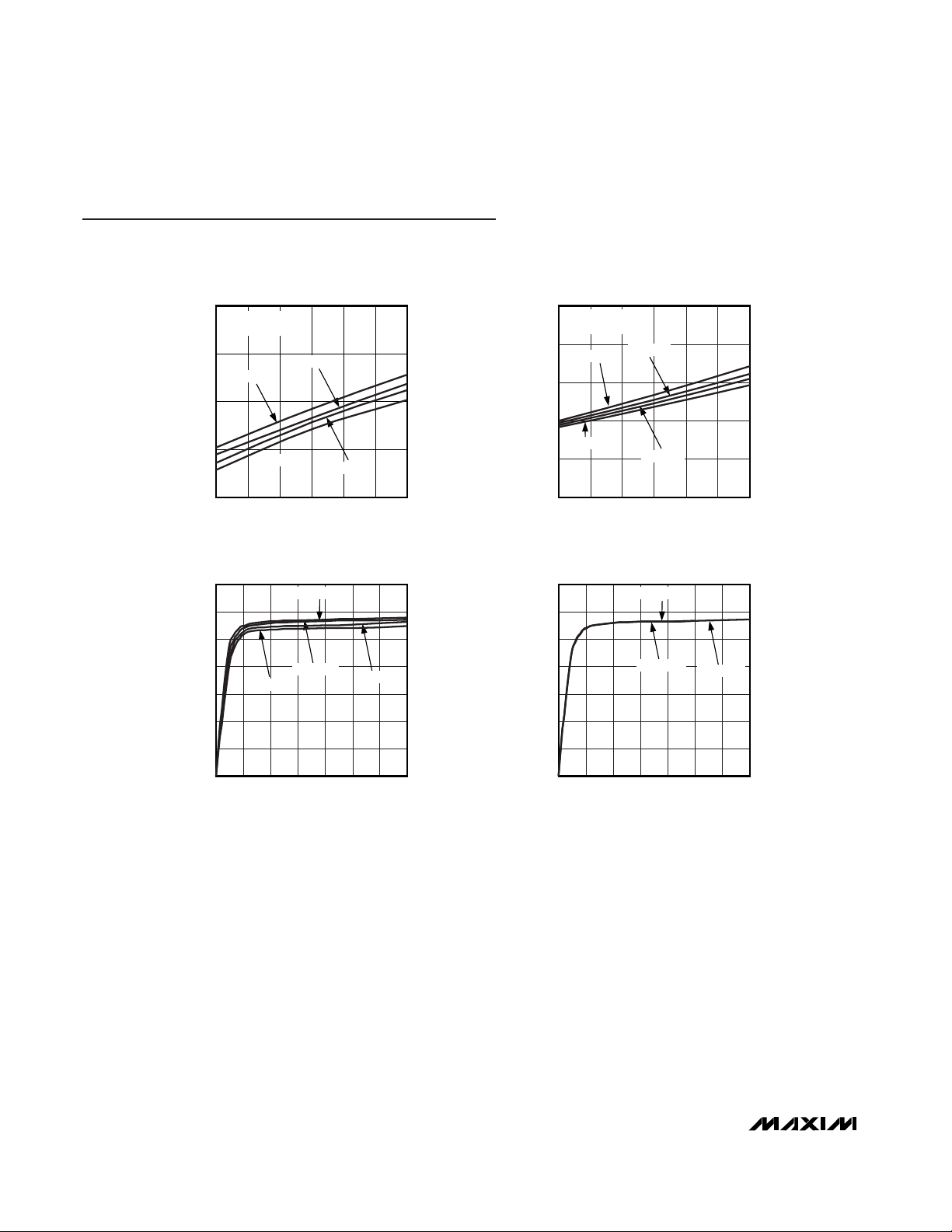
Typical Operating Characteristics
(VDD= 3.3V, TA= +25°C, unless otherwise noted.)
OPERATING CURRENT CONSUMPTION
vs. SUPPLY VOLTAGE V
DD
MAX6972/73 toc01
SUPPLY VOLTAGE VDD (V)
I
DD
(mA)
3.53.43.33.23.1
41
43
45
47
39
3.0 3.6
TA = -40°C
f
CLKI
= 32MHz
CALDAC = 0xFF
TA = +25°C
TA = +85°C
TA = +125°C
OPERATING CURRENT CONSUMPTION
vs. SUPPLY VOLTAGE V
DD
MAX6972/73 toc02
SUPPLY VOLTAGE VDD (V)
I
DD
(mA)
3.53.43.33.23.1
19
21
23
25
15
17
3.0 3.6
TA = -40°C
TA = +25°C
TA = +85°C
TA = +125°C
f
CLKI
= 0MHz
CALDAC = 0x00
LED OUTPUT SINK CURRENT
vs. OUTPUT VOLTAGE
MAX6972/73 toc03
OUTPUT VOLTAGE (V)
I
SINK
(mA)
54321
20
50
60
30
40
70
0
10
067
TA = -40°C
TA = +25°C
TA = +85°C
TA = +125°C
LED OUTPUT SINK CURRENT
vs. OUTPUT VOLTAGE
MAX6972/73 toc04
OUTPUT VOLTAGE (V)
I
SINK
(mA)
54321
20
50
60
30
40
70
0
10
067
VDD = +3.0V
VDD = +3.3V
VDD = +3.6V
Page 5

MAX6972/MAX6973
16-Output PWM LED Drivers
for Message Boards
_______________________________________________________________________________________ 5
Pin Description
PIN NAME FUNCTION
1,17 V
DD
Positive Supply Voltage. Bypass VDD to GND with a 0.1µF ceramic capacitor.
2 MUX0 Multiplex 0 Active-Low, Open-Drain Output. Use MUX0 to drive a pnp transistor.
3 CLKI+ PWM and Serial-Interface Noninverting Clock LVDS Input
4 CLKI- PWM and Serial-Interface Inverting Clock LVDS Input
5 DIN+ Serial-Interface Noninverting Data LVDS Input
6 DIN- Serial-Interface Inverting Data LVDS Input
7 LOADI Serial-Interface Load CMOS Input
8 I.C. Internally Connected. Connect to GND.
9–16 Y0–Y7 Y LED Drive Outputs. Y0 to Y7 are open-drain, constant-current sinks.
18 LOADO Serial-Interface Load CMOS Output
19 DOUT- Serial-Interface Inverting Data LVDS Output
20 DOUT+ Serial-Interface Noninverting Data LVDS Output
21 CLKO- PWM and Serial-Interface Inverting Clock LVDS Output
22 CLKO+ PWM and Serial-Interface Noninverting Clock LVDS Output
23 MUX1 Multiplex 1 Active-Low, Open-Drain Output. Use MUX1 to drive a pnp transistor.
24 AGND Analog Ground. Connect to GND.
25–32 Z7–Z0 Z LED Drive Outputs. Z0 to Z7 are open-drain, constant-current sinks.
EP GND Power Ground. Exposed pad on package underside must be connected to GND.
Page 6
MAX6972/MAX6973
16-Output PWM LED Drivers
for Message Boards
6 _______________________________________________________________________________________
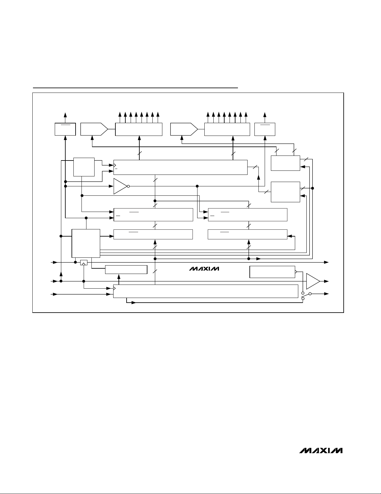
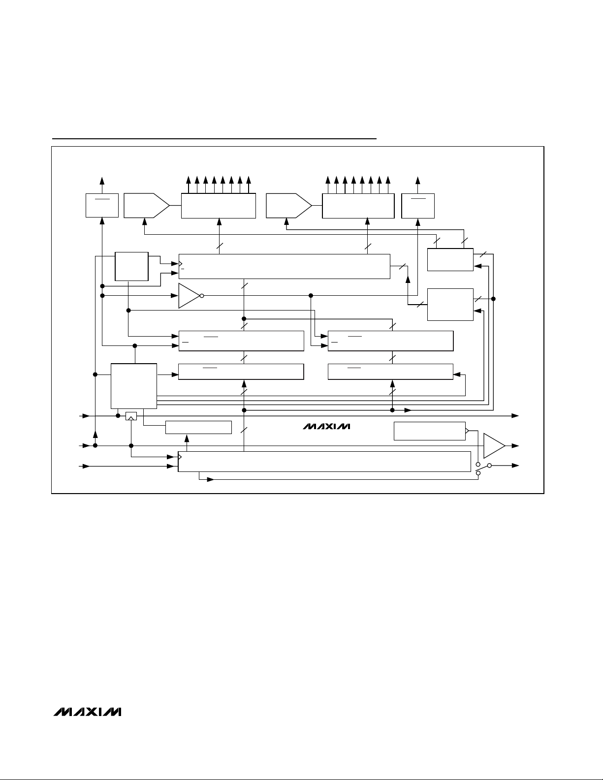
MAX6972 Block Diagram
MUX1
OUTPUT
MUX0
OUTPUT
Y LED DRIVERS
Y7–Y0
I
SET
EXT. PNP
8-BIT
Y CALDAC
Z LED DRIVERS
Z0–Z7
CALIBRATION
DATA LATCH
GLOBAL-
INTENSITY
DATA LATCH
PWM
COUNTERS
SYNC
CONTROL
SYNC DETECT
24-BIT NEW HEADER
SHIFT REGISTER
7-BIT GLOBAL-INTENSITY FRAME MODULATOR
12-BIT INDIVIDUAL INPUT MODULATOR
8
I
SET
8-BIT
Z CALDAC
Y LED OUTPUT
Y7 Y6 Y5 Y4 Y3 Y2 Y1 Y0
Z LED OUTPUT
Z7 Z6 Z5 Z4 Z3 Z2 Z1 Z0
8
8
0/1
8
7
7
192
192 192
192 192
192
192
192
16
7
MUX0 PIXEL PWM OLD DATA LATCH MUX1 PIXEL PWM OLD DATA LATCH
LOAD
OE
LOAD
OE
MUX0 PIXEL PWM NEW DATA LATCH MUX1 PIXEL PWM NEW DATA LATCH
192-BIT DATA SHIFT REGISTER
EN
CLKI
DIN
EN
DOUT
CLKO
LOADO
D
Q1
LOADI
EXT. PNP
MAX6972
Page 7
MAX6972/MAX6973
16-Output PWM LED Drivers
for Message Boards
_______________________________________________________________________________________ 7
MAX6973 Block Diagram
MUX1
OUTPUT
MUX0
OUTPUT
Y LED DRIVERS
Y7–Y0
I
SET
EXT. PNP
8-BIT
Y CALDAC
Z LED DRIVERS
Z0–Z7
CALIBRATION
DATA LATCH
GLOBAL-
INTENSITY
DATA LATCH
PWM
COUNTERS
SYNC
CONTROL
SYNC DETECT
24-BIT NEW HEADER
SHIFT REGISTER
5/3-BIT GLOBAL-INTENSITY PDM MODULATOR
14-BIT INDIVIDUAL PWM MODULATOR
8
I
SET
8-BIT
Z CALDAC
Y LED OUTPUT
Y7 Y6 Y5 Y4 Y3 Y2 Y1 Y0
Z LED OUTPUT
Z7 Z6 Z5 Z4 Z3 Z2 Z1 Z0
8
8
0/1
8
5
5
224
224 224
224 224
224
224
224
16
5
MUX0 PIXEL PWM OLD DATA LATCH MUX1 PIXEL PWM OLD DATA LATCH
LOAD
OE
LOAD
OE
MUX0 PIXEL PWM NEW DATA LATCH MUX1 PIXEL PWM NEW DATA LATCH
224-BIT DATA SHIFT REGISTER
EN
CLKI
DIN
EN
DOUT
CLKO
LOADO
D
Q1
LOADI
EXT. PNP
MAX6973
Page 8

MAX6972/MAX6973
Detailed Description
The MAX6972/MAX6973 drive 16 nonmultiplexed LEDs
or 32 multiplexed LEDs for various indoor and outdoor
display applications. The EZCascade serial interface
enables large multidriver display panels to be constructed with interconnected MAX6972/MAX6973
devices (see Figure 1).
The drivers provide 12-bit (MAX6972) or 14-bit
(MAX6973) individual PWM steps for each LED output.
Four to seven global-intensity bits provide additional
pulse-density modulation (PDM) intensity control (see
Table 1). The MAX6972/MAX6973 provide 19 bits of
total current/intensity control range per color per pixel,
or 18 bits if multiplexing. The total PWM dynamic range
encompasses gamma correction and, if desired, individual LED calibration.
LED outputs are grouped in ports (Y and Z) with eight
LED outputs per port. Each port features its own current calibration control DAC (CALDAC) with 0.31%
resolution to set the current. The MAX6972/MAX6973 current calibration feature allows unmatched LEDS from different lots and manufacturers to be color matched.
Power-Up
On power-up, the MAX6972/MAX6973 set the calibration
current to the minimum current for all LED outputs and
clear the global-intensity PDM data, individual-intensity
PWM data, and the timing counters. The display
remains blank after CLKI starts running. The watchdog
function is inactive after power-up.
16-Output PWM LED Drivers
for Message Boards
8 _______________________________________________________________________________________
HOST
CLKO
DOUT
LOADO
CLKI
DIN
LOADI
MAX6972/
MAX6973
1
MAX6972/
MAX6973
2
MAX6972/
MAX6973
3
MAX6972/
MAX6973
N
CLKI
DIN
LOADI
CLKO
DOUT
LOADO
CLKI
DIN
LOADI
CLKO
DOUT
LOADO
CLKI
DIN
LOADI
CLKO
DOUT
LOADO
CLKI
DIN
LOADI
CLKO
DOUT
LOADO
OPTIONAL FEEDBACK
Figure 1. Generic Cascaded Connection Scheme
GLOBAL PDM
PART
LED DRIVE
OUTPUTS
LED DRIVE
CURRENT
CALIBRATION
DIRECT MULTIPLEXED
INDIVIDUAL
PWM
MAX6972 7 bits 6 bits 12 bits
5 bits 4 bits
MAX6973
16
(7V rated)
55mA
3 bits 2 bits
14 bits
Table 1. Comparison of MAX6972/MAX6973
DAC RANGE
11mA to 55mA
Page 9

LED Intensity Control
The MAX6972/MAX6973 provide three levels of output
current control for LED drive: calibration DACs
(CALDACs), global-intensity control, and individualintensity control. The CALDACs set the port output current levels, while the global-intensity and individualintensity controls modulate the output current on/off
times, providing a fine-resolution control of average
output currents (see Figure 2). The individual-intensity
control operates on each output independently to set
each individual LED intensity level. The global-intensity
controls modulate MAX6972/MAX6973 outputs simultaneously for a uniform brightness control without affecting color. Using a fixed output current level that is
modulated only by on/off control leaves the LED color
unaffected while precisely controlling intensity. Finally,
all outputs can be turned on and off simultaneously by
setting or clearing configuration bit D3 (PWM-ON).
Calibration DACs
The 8-bit Y and Z CALDACs set the output current level
for all 8 outputs in the Y and Z ports, respectively (see
the MAX6972/MAX6973 Block Diagrams). The Y
CALDAC and Z CALDAC range from a low of 11mA
(0x00) to a maximum of 55mA (0xFF), providing
172µA/step of current trimming. The CALDACs are
loaded by the serial interface using command 01 (see
Table 4). The Z CALDAC data is loaded first, followed
by the Y CALDAC data (see the Serial Interface section).
The loaded data takes effect immediately.
Global-Intensity Control
The MAX6972/MAX6973 adjust global and individual
intensities over a time period called a frame. One frame
requires 219(524,288) periods of CLKI and corresponds to one video-frame time. Video frames generally
contain consecutive images displayed rapidly to yield
a motion picture display. Running the MAX6972/
MAX6973 at f
CLKI
= 31.5MHz allows a video-frame
update rate of 60fps for full-motion video (see the
MAX6972 Video-Frame Timing and MAX6973 VideoFrame Timing sections).
The MAX6972/MAX6973 further divide frames into subframes to allow a unique combination of global- and
individual-intensity controls. The number of subframes
is equal to the number of global-intensity control steps.
The MAX6972 uses 128 subframes per frame in
nonmultiplexed mode (corresponding to 7-bit globalintensity PDM control) and 64 subframes in multiplexed
mode (corresponding to 6-bit global-intensity PDM
control). The MAX6973 features 5-, 4-, 3-, and 2-bit
global-intensity control to yield 32, 16, 8, and 4 subframes per frame, respectively.
The MAX6972/MAX6973 control global intensity by
driving subframes on and off. When a subframe is on, it
allows the individual PWM intensity control to be driven
on the outputs. Subframes that are off do not have any
PWM modulation on the outputs.
MAX6972/MAX6973
16-Output PWM LED Drivers
for Message Boards
_______________________________________________________________________________________ 9
10
20
30
50
(mA)
CALDAC
CURRENT
40
55mA MAX
11mA MIN
1270
GLOBAL
= 96
GLOBAL-INTENSITY
PDM
INDIVIDUAL-INTENSITY
PWM
40950
Yn or Zn PWM
= 2560
Yn or Zn I
AVE
= 18.750mA
CALDAC
= 169
2550
40mA
100%
0%
50%
100%
0%
50%
100%
0%
50%
Figure 2. Relationship Among the CALDACs, Global-Intensity, and Individual-Intensity PWM Controls
Page 10

MAX6972/MAX6973
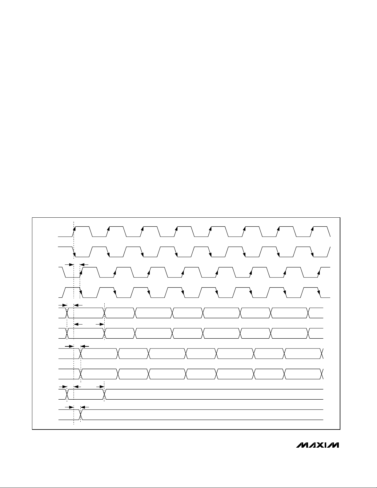
Individual PWM Control
The MAX6972/MAX6973 further modulate the time that
each subframe is ON by a pulse-width modulation
(PWM) value. Each output current driver in the Y and Z
ports has a unique 12-bit (MAX6972) or 14-bit
(MAX6973) PWM control value providing fine resolution
adjustment of average current output. Each bit time of
the PWM corresponds to one period of CLKI (T
CLKI
).
The PWM setting determines the amount of time (out of
the total period) that the output is on. The subframes
have PWM off zones at the start (t
SPWM
) and end
(t
EPWM
) of the PWM period (see Figure 3). The subframe period and PWM off zones are shown in Table 2
for each device.
The MAX6972 subdivides each subframe by 4096
(12-bit) PWM steps and has 16 cycle off zones, leaving
an active PWM region of 4064 PWM steps ranging from
16 to 4079. The MAX6973 subdivides each subframe by
16,384 (14-bit) PWM steps and has 32 cycle off zones,
leaving an active PWM region of 16,320 PWM steps
ranging from 32 to 16,351. The PWM phase for outputs
Y0, Y2, Y4, Y6 and Z0, Z2, Z4, Z6 use phasing with the
outputs on first and off second. Inverse phasing is used
for outputs Y1, Y3, Y5, Y7 and Z1, Z3, Z5, Z7 to balance
the timing of loads on the LED anode power supply, as
shown in Figure 3.
In multiplexed operation, the subframes are shared
between MUX0 and MUX1 active times, effectively
reducing the number of subframes by 2.
LED-Intensity Control Example
The three levels of intensity control are shown in Figure 2
for one LED output driver in a MAX6972 in nonmultiplexed mode. As an example, the CALDAC is set to
169
DEC,
setting the port output current level to 40mA.
16-Output PWM LED Drivers
for Message Boards
10 ______________________________________________________________________________________
Y0, Y2, Y4, Y6
Z0, Z2, Z4, Z6
Y1, Y3, Y5, Y7
Z1, Z3, Z5, Z7
Y0, Y2, Y4, Y6
Z0, Z2, Z4, Z6
Y1, Y3, Y5, Y7
Z1, Z3, Z5, Z7
SUBFRAME (n) SUBFRAME (n + 1)
t
SPWM
t
EMUX
t
EMUX
MUX0
SUBFRAME (n), MUX0 SUBFRAME (n), MUX1
MUX1
t
SPWM
t
SPWM
t
EPWM
MULTIPLEXED
NONMULTIPLEXED
t
SPWM
t
EPWM
ON/OFF PHASING
OFF/ON PHASING
ON/OFF PHASING
OFF/ON PHASING
50% 75%
100%25%
75%75%
75% 75%
Figure 3. Multiplexed and Nonmultiplexed Output Driver Phasing and Example PWM Values
PART
SUBFRAME
(T
CLKI
)
t
SPWM
t
EPWM
t
EMUX
(T
CLKI
)
4096 16 16 16
16,384 32 32 32
Table 2. Subframe and PWM Timing
(T
)
(T
CLKI
MAX6972
MAX6973
CLKI
)
Page 11

The global-intensity PDM value is set to 96
DEC
, producing
an even distribution of ON subframes out of the 128 possible (shown in Figure 4 as subframes 1, 3, 4, 5, etc).
Each subframe can be ON for a PWM duration set by the
individual PWM value. The PWM value setting of
2560
DEC
out of 4096 (12-bit) results in a further reduction
of current ON time (shown in bold trace).
The internal PDM logic spreads the on subframes as
evenly as possible among the off subframes to keep
the effective scanning frequency high.
For applications with a slower clock speed, the
MAX6973 can increase the display refresh rate by a
factor of four to eliminate visible flicker. Setting configuration bit D4 (GLB4) to 1 activates the increased
refresh rate (see Table 6). The increased refresh rate
reduces the number of global-intensity settings by a
factor of four (see Table 3).
MAX6972 Video-Frame Timing
The MAX6972 supports up to 60 video frames per
second (fps). The following equation shows the
required clock frequency to support 60 video fps:
60 (video fps) x 4096 (clocks per 12-bit PWM period) x
128 (global-intensity subframes) = 31.5MHz.
The MAX6972 supports up to a 33MHz clock signal
(~63fps).
Each 12-bit PWM period contains 4096 clock cycles;
multiply that number by 128 (number of global intensity
subframes) to obtain the required number of clock cycles
(524,288) per video frame. The MAX6972 requires 36
bits (12 bits per color multiplied by three colors) to drive
an RGB pixel. The maximum pixel data that the
MAX6972 can send per video frame is 524,288 / 36 or
14,563 pixels, corresponding to 2730 cascaded
MAX6972s.
MAX6973 Video-Frame Timing
The MAX6973 also supports up to 60 video frames per
second (fps). The following equation shows the
required clock frequency to support 60 video fps:
60 (video fps) x 16,384 (clocks per 14-bit PWM period)
x 32 (global-intensity subframes) = 31.5MHz.
The MAX6973 supports up to a 33MHz clock signal
(~63fps).
Each 14-bit PWM period contains 16,384 clock cycles;
multiply 16,384 by 32 (global-intensity subframes) to
obtain the required number of clock cycles (524,288)
per video frame. The MAX6973 requires 42 bits (14 bits
per color multiplied by three colors) to drive an RGB
pixel. The maximum pixel data that the MAX6973 can
send per video frame is 524,288 / 42 or 12,483 pixels,
corresponding to 2340 cascaded MAX6973s.
MAX6972/MAX6973
16-Output PWM LED Drivers
for Message Boards
______________________________________________________________________________________ 11
169d = 40
SUBFRAME NUMBER
10
20
30
50
55mA MAX
11mA MIN
(mA)
01234567891011
CALDAC CURRENT
OUTPUT LED CURRENT
PWM = 2560/4096
ONE FRAME IS 219 (524,288) CLKI CYCLES LONG
GLOBAL PDM = 96/128 SUBFRAMES
ON ON ON ON ON ON ON ON
Figure 4. The three levels of LED current control (CALDAC, global-intensity PDM, and individual PWM) modulate the average output
current.
Page 12

MAX6972/MAX6973
Multiplexed vs. Nonmultiplexed Operation
The MAX6972/MAX6973 can double the number of
LEDs driven from 16 to 32 through multiplexing. When
multiplexing, the two outputs, MUX0 and MUX1, drive
two external pnp transistors, such as FMMTL717, used
as common-anode power switches (see Figure 5).
16-Output PWM LED Drivers
for Message Boards
12 ______________________________________________________________________________________
Y0Y1Y2Y3Y4Y5Y6
Y7
+5.55V
Q1
FMMTL717
(REDS)
(REDS)
(GREENS)
(GREENS)
R1
560Ω
R2
180Ω
C1
120pF
+5.55V
Q1
FMMTL717
R1
560Ω
R2
180Ω
C1
120pF
Z1Z2Z3Z4Z5Z6Z7
Z0
SUBFRAME 31
MUX1
16,384 CLKs
SUBFRAME 0
MUX0
16,384 CLKs
SUBFRAME 0
MUX1
16,384 CLKs
SUBFRAME 1
MUX0
16,384 CLKs
SUBFRAME 1
MUX1
16,384 CLKs
SUBFRAME 14
MUX0
16,384 CLKs
SUBFRAME 14
MUX1
16,384 CLKs
SUBFRAME 15
MUX0
16,384 CLKs
SUBFRAME 15
MUX1
16,384 CLKs
SUBFRAME 0
MUX0
16,384 CLKs
ONE COMPLETE 524,288 CLOCK CYCLE NONMULTIPLEXED VIDEO FRAME
MUX0
MUX1
Figure 5. MAX6973 Multiplexing Two Sets of Eight RG Pixels with a Single LED Supply and Subframe Timing
Page 13

Setting configuration bit D0 to 1 enables multiplex
operation. MUX0 and MUX1 alternate the LED anode
drive voltage between two sets of LEDs. The Y and Z
ports provide individual PWM control during alternate
MUX cycles as shown in Figure 3. The alternating MUX
cycles reduce the global-intensity resolution (the number of subframes) by half, which reduces the average
LED current by half.
Watchdog
A selectable watchdog timer monitors serial-interface
inputs CLKI, DIN, and LOADI. Enabling the watchdog
timer requires that CLKI, DIN, and LOADI toggle at
least once every 40ms. If any of these transitions fails to
occur, then the individual-intensity PWM data latches
clear. This condition effectively blanks the LEDs.
Update the individual-intensity PWM data registers to
turn the LEDs back on. The watchdog timeout does not
affect the calibration or global-intensity data, the clock
synchronization, or multiplexed/nonmultiplexed setting.
Use the watchdog functionality in safety-critical applications where a blanked display is safer than an incorrect display.
LED Open-Circuit and
Overtemperature Detection
The MAX6972/MAX6973 feature two fault detection functions: open-circuit LED outputs and overtemperature. An
LED open-circuit is detected on driver outputs by monitoring for output voltages below 200mV. When an open
circuit is detected, the MAX6972/MAX6973 increments
a fault counter included in the serial-interface protocol
that can be routed back to the host transmitter for diagnostics. Any number of open-circuit LEDS, multiplexed
or nonmultiplexed, can be detected, however only one
counter increment occurs per device.
The MAX6972/MAX6973 detect die temperatures
above T
DIE
= +165°C and disable all output drivers by
setting all PWM data to zero. The fault counter in the
serial-interface protocol is incremented by one count
for each cascaded device with an overtemperature
condition. The output drivers are turned back on when
the die temperature falls below T
DIE
= +150°C. The
fault counter value is distinguished between LED opencircuit and overtemperature conditions by the serialinterface command used at the time of detection (see
the Serial Interface section for more details).
MAX6972/MAX6973
16-Output PWM LED Drivers
for Message Boards
______________________________________________________________________________________ 13
PART
PWM
RES.
TOTAL CLOCKS PER
PWM SUBFRAME
USEABLE CLOCKS PER
PWM SUBFRAME
MAXIMUM PWM
DUTY CYCLE
0
1 Multiplex
12 bits 4096 4064 4064 / 4096 = 99.22%
0
1 Multiplex
14 bits 16,384 16,320
16,320 / 16,384 = 99.61%
Table 3. MAX6972/MAX6973 Timing Comparison
PART
GLB4
MUX
OPERATION
GLOBAL
PDM
RES.
SUBFRAMES
CLOCKS
PER
CLOCK
FOR 50fps
CLOCK
FREQUENCY (MHz)
FOR 60fps
X0
7 bits 128
X1Multiplex 6 bits 64
26.2144 31.45728
0
5 bits 32
0
1 Multiplex 4 bits 16
26.2144 31.45728
0
3 bits 8
1
1 Multiplex 2 bits 4
6.5536 7.8643
MAX6972
MAX6973
MAX6972
MAX6973
MUX
BIT
BIT
OPERATION
Nonmultiplex
Nonmultiplex
BIT
Nonmultiplex
Nonmultiplex
Nonmultiplex
PER FRAME
FREQUENCY (MHz)
FRAME
524,288
524,288
131,072
Page 14

MAX6972/MAX6973
Commands
The MAX6972/MAX6973 have four commands used to
load all operating mode and LED output current data.
Each command is uniquely identified by two bits, C1
and C0, embedded in the serial-interface protocol
structure. The commands Load CALDAC, Load GlobalIntensity PDM, and Load Configuration each require 16
bits of data (2 bytes) for every cascaded device. The
number of bits required for the command load individual
PWM varies by device and multiplex mode of operation.
Each cascaded device can receive unique data for
CALDACs, global intensity, configuration, and individual
PWM output drivers. Generally, all cascaded devices
are operated in the same configuration mode. The data
bytes are transmitted MSB first for all commands. The
commands are communicated to all cascaded devices
by the host using the synchronous serial-interface and
protocol structure (see the Serial Interface section for
details). The four commands and the data lengths for
each command are shown in Table 4.
The MAX6972, operating in nonmultiplexed mode,
requires sixteen 12-bit individual PWM data (192 bits
total) and requires thirty-two 12-bit data (384 bits total)
in multiplexed operation mode. Similarly, the MAX6973
operating in nonmultiplexed mode requires sixteen 14-bit
individual-intensity PWM data (224 bits total) and
requires thirty-two 14-bit (448 bits total) data in multi-
plexed mode. The individual PWM data are loaded into
an intermediate latch and transferred to the actual
PWM latches at subframe 0 and PWM clock 0.
Both Y and Z calibration DACs are loaded with 8-bit
data each in nonmultiplexed and multiplexed modes.
Data is updated immediately into the CALDAC latches
(see Table 8).
The MAX6972/MAX6973 require one data byte to set the
global-intensity PDM for all output drivers. The globalintensity PDM data has a variable number of active bits
depending on the multiplex operating mode and, for
the MAX6973, the global-quarter setting. The number of
bits used for global-intensity control is always justified
to the LSB of the data byte, as shown in Table 5. One
byte of data is sent twice with the global-intensity PDM
data bits justified to the LSB. Data is updated into the
PWM latches at subframe 0 and PWM clock 0 (see
Table 9).
When using the MAX6973 5-bit global-intensity setting,
the settings range from 0 to 63 to set the global intensity
from 1 to 64 subframes ON to 64 out of 64 subframes ON.
When using the MAX6972 7-bit global-intensity setting,
the settings range from 0 to 127 to set the global intensity from 1 out of 128 subframes ON to 128 out of 128
subframes ON.
16-Output PWM LED Drivers
for Message Boards
14 ______________________________________________________________________________________
CMD[1:0]
C1 C0
COMMAND
DATA LENGTH PER CASCADED DEVICE
192 bits (MAX6972 nonmultiplexed)
384 bits (MAX6972 multiplexed)
224 bits (MAX6973 nonmultiplexed)
00Load individual PWM
448 bits (MAX6973 multiplexed)
01Load CALDAC 16 bits
10Load global-intensity PDM 16 bits
11Load configuration 16 bits
Table 4. Commands and Data Length
PART
D6 D5 D4 D3 D2 D1
LSB D0
X0 70Bit[6] Bit[5] Bit[4] Bit[3] Bit[2] Bit[1]
Bit[0]
X1 600Bit[5] Bit[4] Bit[3] Bit[2] Bit[1]
Bit[0]
00 5000Bit[4] Bit[3] Bit[2] Bit[1]
Bit[0]
01 40000Bit[3] Bit[2] Bit[1]
Bit[0]
10 300000Bit[2] Bit[1]
Bit[0]
11 2000000Bit[1]
Bit[0]
Table 5. Global-Intensity Data Bit Justification
MAX6972
MAX6973
GLB4 MUX TOTAL BITS MSB D7
Page 15

The global-intensity data is received in an intermediate
register and is applied to the outputs at subframe 0 and
PWM clock 0.
The MAX6972/MAX6973 have one byte of configuration
data with 5 active bit settings as shown in Table 6. One
byte of data containing configuration bit settings is sent
twice. Data is updated immediately into the CALDAC
latches. See Table 10. The loaded configuration settings
take effect immediately.
Serial Interface
The MAX6972/MAX6973 feature a fully synchronous
and fully buffered serial interface that allows cascading
of multiple devices. The serial interface consists of
inputs (CLKI, DIN, and LOADI) and outputs (CLKO,
DOUT, and LOADO). The MAX6972/MAX6973 can
pass different data to each cascaded device without
any additional inputs to identify the position of the
devices in the cascaded chain.
MAX6972/MAX6973
16-Output PWM LED Drivers
for Message Boards
______________________________________________________________________________________ 15
DESCRIPTION
MSB D7 — 0 Not used
D6 — 0 Not used
D5 — 0 Not used
D4 GLB4
Enables the reduced global-intensity setting in the MAX6973 when set to
1. When set, the MAX6973 uses eight (or four, if multiplexing) PWM
subframes. GLB4 is set to 0 as power-on default. Setting bit D4 has no
effect in the MAX6972.
D3 PWM-ON
Enable
individual
PWMs
Turns all individual PWM outputs on when set to 1. Power-on default is
PWM-ON set to 0 to disable all current output drivers. PWM-ON can be
used to turn all LEDs on or off without affecting the global-intensity or
individual PWM settings.
D2 CRST
Reset frame
and PWM
counters
Setting CRST to 1 synchronously resets internal counters to 0. This action
sets the MAX6972/MAX6973 to subframe 0 of the global-intensity
subframe counter and clock 0 of all individual PWM counters. The CRST
bit is a nonlatching control function that resets to 0 after the counters are
set to 0.
D1 WDOG
Watchdog
enable
Setting WDOG to 1 enables the watchdog timer operation. Power-on
default is 0.
LSB D0 MUX
Multiplex
enable
Setting MUX to 1 turns multiplex mode on. Power-on default is 0.
Table 6. Load Configuration Bit Definitions
CONFIGURATION BIT ACRONYM FUNCTION
Global quarter
Page 16
MAX6972/MAX6973
The serial interface uses the continuously running
clock, CLKI, to synchronously transfer and latch data
(33MHz max). The MAX6972/MAX6973 sample inputs
DIN and LOADI on the rising edge of CLKI and update
outputs DOUT and LOADO on the edge of CLKI. The
MAX6972/MAX6973 specifications guarantee that cascaded devices observe setup and hold timing from
device to device, making external buffers and clock
trees unnecessary, even in very large systems.
The high-speed CLKI, CLKO, DIN, and DOUT signals
use low-voltage differential signaling (LVDS), and the
less frequently changing control signals, LOADI and
LOADO, use standard CMOS. The differential signals
are generally referred to in unipolar shorthand; for
example, the statement “CLKI rising edge” means that
CLKI+ is rising, and CLKI- is falling.
The MAX6972/MAX6973 use LVDS drivers with differential
signaling (300mV nominal logic swing around a +1.2V
bias) and cascaded CMOS control signals to minimize
signal-path EMI and simplify interface timing and PC
board layout. Note the differential inputs for the first driver can be driven from +3.3V CMOS using LVDS level
translators, such as the MAX9112 terminated with 110Ω
(see Figure 12).
A 25MHz to 33MHz clock frequency is recommended
to keep the display refresh rate high. When using the
MAX6973 in reduced global-intensity mode (GLB4 = 1
in configuration register), the recommended clock
frequency range is 6MHz to 33MHz.
Serial-Interface Protocol Structure
The MAX6972/MAX6973 serial interface transfers all
data and control functions using a protocol structure
consisting of header, data, and optional tail segments
transmitted in this sequence. The header and tail
segments transfer to all cascaded devices, while the
data section reduces in bit length as data transfers
16-Output PWM LED Drivers
for Message Boards
16 ______________________________________________________________________________________
t
HD-DIN
t
HD-LOADI
CLKI+
CLKI-
CLKO+
CLKO-
DIN+
DIN-
DOUT+
DOUT-
LOADI
LOADO
t
PD-CLKO
t
SU-DIN
t
PD-DOUT
t
PD-LOADO
t
SU-LOADI
Figure 6. Serial-Interface Timing
Page 17
through the cascaded devices. When LOADI is low, the
MAX6972/MAX6973 continuously monitor DIN for
reception of the SYNC pattern (see the Header
Segment section).
Header Segment
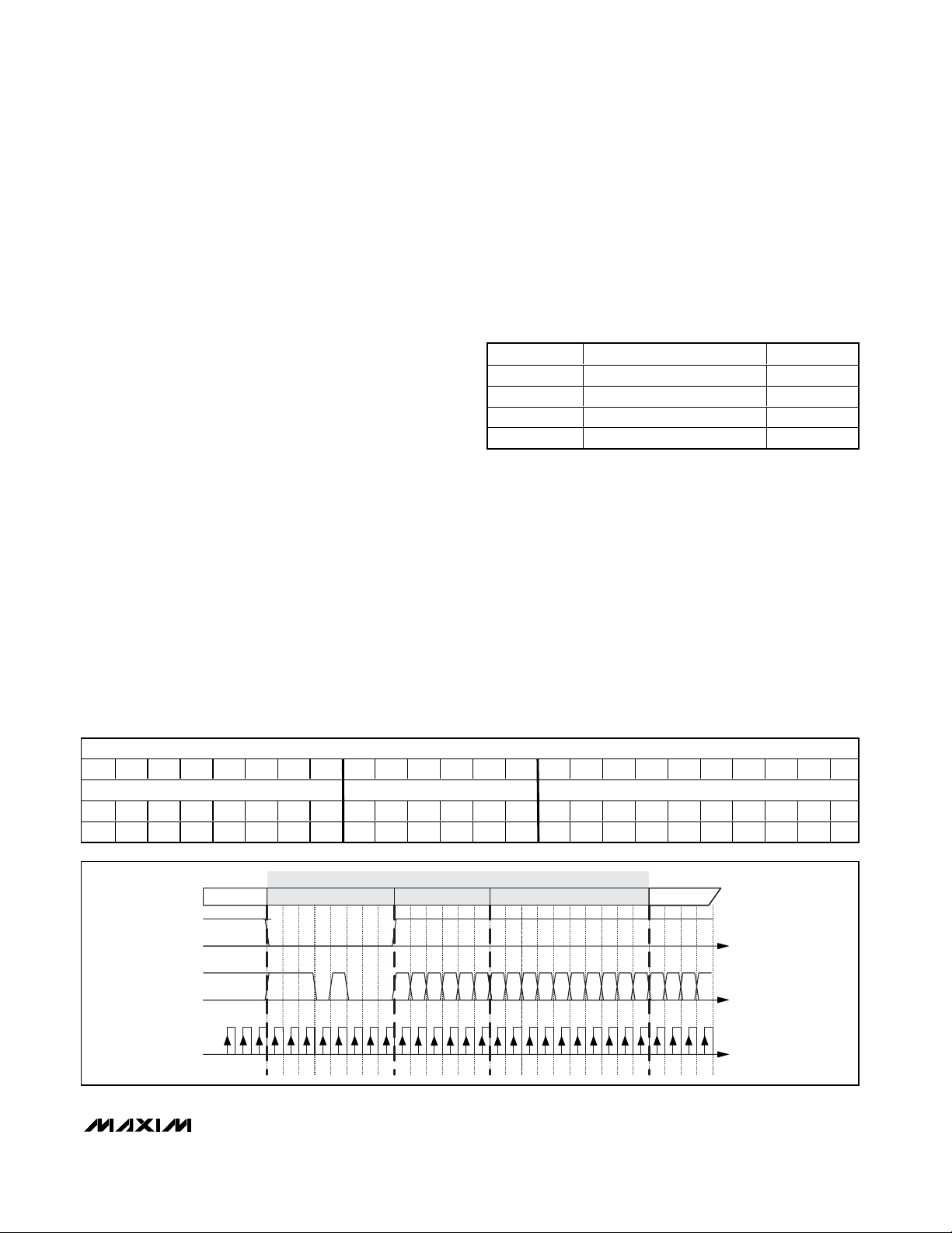
The 24-bit header segment consists of an 8-bit fixed
synchronization pattern (SYNC), a 6-bit command pattern (CMD), and a 10-bit counter (CNTR) segment (see
Table 7). LOADI must change from low to high within
plus or minus one clock cycle of the first command bit.
When the SYNC bit pattern 0xE8 is recognized, LOADI
is monitored for the rising edge, allowing the device to
internally synchronize LOADI to CLKI. The six command
bits, CMD[5:0], consist of bits C1 and C0 repeated
three times. The four commands used by the MAX6972/
MAX6973 are defined by the two bits, C1 and C0.
The counter segment is incremented by one for each
cascaded device with an internal fault detected. Use the
counter segment to collect fault data across the cascaded chain.
HDR[23:0]
Complete 24-bit header segment.
SYNC[7:0]
Synchronization bit pattern 0xE8 is recognized by the
MAX6972/MAX6973 during intervals when LOADI is low.
The SYNC bit pattern, followed by the rising edge of
LOADI, internally synchronizes the timing relationship
between CLKI and DIN with the LOADI signal. The
synchronization pattern must be 0xE8.
CMD[5:0]
Send command bits C1 and C0 three times in succession. The command bits define how many data bits are
received and where the data is loaded. The four commands are:
CNTR[9:0]
This is the counter for open LED or overtemperature fault
conditions. The host sends the header segment with the
counter value set to zero. The counter value is incremented one count by each device that detects a fault
condition in the cascaded chain. The accumulated count
value returns to the host from the last device in the cascade chain. The command determines which fault type
is incremented to the counter (see LED Open-Circuit and
Overtemperature Detection Counter section):
CMD[1:0] = X0 Overtemperature faults counted
CMD[1:0] = X1 Open LED faults counted
MAX6972/MAX6973
16-Output PWM LED Drivers
for Message Boards
______________________________________________________________________________________ 17
HDR
0
SYNC CMD CNTR
0
b0
Table 7. Serial-Interface Header
C1:C0 COMMAND CMD[5:0]
00 Load individual PWM 000000
01 Load CALDAC 010101
10 Load global-intensity PDM 101010
11 Load configuration 111111
Figure 7. Header-Segment Timing
23 22 21 20 19 18 17 16 15 14 13 12 11 10 9 8 7 6 5 4 3 2 1
76543210101010987654321
11101000C1C0C1C0C1C0b9b8b7b6b5b4b3b2b1
LOADI
DIN
CLKI
(CONTINUOUS)
1
0
11101000
1
2
HEADER
SYNC
4
3
5
6
7
COMMAND
C1 C0 C1 C0 C1 C0
10
11
8
9
b9 b8 b7 b6 b5 b4 b3 b2
13
12
14
15
COUNTER
b1 b0
16
19
18
17
20
21
22
23
DATA
24
26
25
27
28
Page 18

MAX6972/MAX6973
Data Segment
The bit length of the data segment received by the
MAX6972/MAX6973 is dependent on the command
specified in the header.
The load CALDAC command has two unique data
bytes, while load global-intensity PDM and load
configuration each have one byte of data repeated
once. The CALDAC data within the command load
CALDAC is sent with Z CALDAC data first followed by
Y CALDAC data, as shown in Table 8.
The data segment of the load individual PWM command
has a variable length depending on specific device and
configuration settings. The data is always organized
as Z driver data first in the order of Z7 first to Z0 last
(MSB first), followed by the Y driver data in the same
order of Y7 to Y0 (MSB first).
Tail Segment
The MAX6972/MAX6973 allow for an optional string of
data bits to be transmitted following all device data
bits, which is referred to as the tail segment. The data
bits of the tail segment are clocked back to the host,
following the header, from the last device in a cascaded
chain. The number of bits in the tail segment is optional.
The tail carries no device-specific data on DIN, but
provides feedback confirmation to the host that all data
bits were extracted by all devices in the cascade chain.
16-Output PWM LED Drivers
for Message Boards
18 ______________________________________________________________________________________
HEADER DATA 1 DATA 2 DATA 3 … DATA N
HDR[23:0] Z[7:0] Y[7:0] Z[7:0] Y[7:0] Z[7:0] Y[7:0] … Z[7:0] Y[7:0]
Table 8. Serial Format for Load CALDAC
HEADER DATA 1 DATA 2 DATA 3 … DATA N
HDR[23:0] D[7:0] D[7:0] D[7:0] D[7:0] D[7:0] D[7:0] … D[7:0] D[7:0]
Table 9. Serial Format for Load Global-Intensity PDM
HEADER DATA 1 DATA 2 DATA 3 … DATA N
HDR[23:0] D[7:0] D[7:0] D[7:0] D[7:0] D[7:0] D[7:0] … D[7:0] D[7:0]
Table 10. Serial Format for Load Configuration
HEADER DATA 1 DATA 2 DATA 3 … DATA N
HDR[23:0] Z7, Z6, …Y0 Z7, Z6, …Y0 Z7, Z6, …Y0 … Zn…Yn
Table 11. Serial Format for Load Individual PWM (Nonmultiplexed)
HEADER DATA 1 DATA 2 DATA 3 … DATA N
HDR[23:0]
…
Z7, Z7', Z6, Z6', …Y0'
Table 12. Serial Format for Load Individual PWM (Multiplexed)
Z[7:0] 8-bit data loaded into port Z CALDAC
Y[7:0] 8-bit data loaded into port Y CALDAC
N Number of cascaded devices
D[7:0] Send the same data repeated (16 total bits) for the 8-bit data for global-intensity PDM
Send the 8-bit data for the global-intensity PDM twice (16 total bits)
D[7:0] Send the same data repeated (16 total bits) for the 8-bit data for configuration
Send the 8-bit configuration data two times (16 total bits)
Z_…Y_ 12-bit (MAX6972) or 14-bit (MAX6973) data each
Z_ 12-bit (MAX6972) or 14-bit (MAX6973) PWM data for each output Z_ during multiplex phase MUX0, MSB first
Z_' 12-bit (MAX6972) or 14-bit (MAX6973) PWM data for each output Z_ during multiplex phase MUX1, MSB first
Y_ 12-bit (MAX6972) or 14-bit (MAX6973) PWM data for each output Y_ during multiplex phase MUX0, MSB first
Y_' 12-bit (MAX6972) or 14-bit (MAX6973) PWM data for each output Y_ during multiplex phase MUX1, MSB first
Z7, Z7', Z6, Z6', …Y0' Z7, Z7', Z6, Z6', …Y0' Z7, Z7', Z6, Z6', …Y0'
Page 19

Serial-Interface Cascade Timing
The MAX6972/MAX6973 serial-interface protocol timing
is simplified by the guaranteed setup and hold characteristics of the outputs from one device driving the
inputs of another. An example of a cascade of three
MAX6972/MAX6973 devices is shown in Figure 8.
Example of Serial-Interface
Cascade Timing
The basic timing of a MAX6972/MAX6973 cascaded
chain of three devices demonstrates the principle that
applies to any number of cascaded devices. The first
device connected to the host transmitter is referenced
as 1, and the remaining devices are referenced as 2
and 3. Device 3 outputs connect to the host for communicating diagnostic and fault counter data.
The first MAX6972/MAX6973, device 1, receives the
header and captures the first set of data bits. The
number of captured bits is determined by the command
given in the header. A timing example of the data transfer for the Load CALDAC command is shown in Figure
9. Device 1 does not send the captured data out on
DOUT. Instead, device 1 sends out a new header 17
clock cycles after the reception of the first header bit on
DIN. The data flow on each interconnect node is shown
in Figure 10.
After capturing the first data set, device 1 transmits all
following data segments and the optional tail segment
on DOUT, delayed by one CLKI cycle. Device 2
receives the new header from device 1, followed by
data that now begins with device 2’s data set. Device 2
repeats the same process as described above; capturing the first data set received, appending a new header, and passing all subsequent data out DOUT to the
next device 3. Device 3 captures the last data set and
transmits a header followed by the tail segment. The
last header and tail segments are clocked back into the
host receiver. The header received by the host contains
the updated fault counter data. The tail data bit pattern
can be compared to the tail data originally transmitted
by the host for data integrity check.
When the MAX6972/MAX6973 send individual-intensity
PWM data, the data segment bit length is large due to
MAX6972/MAX6973
16-Output PWM LED Drivers
for Message Boards
______________________________________________________________________________________ 19
HOST
CLKO
DOUT
LOADO
CLKI
DIN
LOADI
CLK0
D0
LOAD0
CLK1
D1
LOAD1
CLK2
D2
LOAD2
CLK3
D3
LOAD3
MAX6972/MAX6973
1
MAX6972/MAX6973
2
MAX6972/MAX6973
3
CLKI
DIN
LOADI
CLKO
DOUT
LOADO
CLKI
DIN
LOADI
CLKO
DOUT
LOADO
CLKI
DIN
LOADI
CLKO
DOUT
LOADO
Figure 8. Example Showing Three-Device Cascade Connection Scheme with the Interconnecting Nodes Labeled for Clarity
DATA: CALDAC DATA 1
(CONTINUOUS)
25
26
27
28
29
30
31
32
33
34
35
36
37
38
39
40
41
42
43
44
45
46
47
48
49
50
51
52
53
54
55
56
57
58
59
60
61
62
63
64
65
66
67
68
69
70
71
72
CLKI
LOADI
DIN
0
1
DATA: CALDAC DATA 2
Z CALDAC Y CALDAC Z CALDAC Y CALDAC Z CALDAC Y CALDAC
DATA: CALDAC DATA 3
D7 D6 D5 D4 D3 D2 D1 D0
D7 D6 D5 D4 D3 D2 D1 D0 D7 D6 D5 D4 D3 D2 D1 D0 D7 D6 D5 D4 D3 D2 D1 D0 D7 D6 D5 D4 D3 D2 D1 D0 D7 D6 D5 D4 D3 D2 D1 D0
Figure 9. Timing Example Showing CALDAC Data Set for Three Cascaded Devices
WORD 1 WORD 2 WORD 3HEADER 1
T
WORD 2 WORD 3HEADER 2
T
WORD 3HEADER 3
T
HEADER 4
T
17 CLOCKS
17 CLOCKS
17 CLOCKS
CLK0
D0
D1
D2
D3
Figure 10. Data Cascading Example for 16-Bit Data Words
Page 20

MAX6972/MAX6973
the 12-bit or 14-bit PWM data for each of the 16 outputs
(see Figure 11). The various data segment bit lengths
for each of the four commands and different operating
modes is shown in Table 4. Data capturing is the same
as described above with the header segment outputs
and data being delayed by the full length of the data bit
stream being captured plus one clock cycle.
LED Open-Circuit and
Overtemperature Detection Counter
The MAX6972/MAX6973 feature LED open-circuit
detection and overtemperature detection that use the
counter section of the header segment to record
detected faults. Using commands 01 or 11 force the
counter to record LED open-circuit detection faults.
Using commands 00 or 10 force the counter to record
overtemperature faults.
The MAX6972/MAX6973 detect an open circuit on a driver
output by monitoring for output voltages below 200mV.
When an open circuit is detected, the MAX6972/
MAX6973 increment the counter segment data,
CNTR[9:0], received on DIN by 1 before transmitting a
header and new counter value out DOUT. Regardless
of the number of open-circuit outputs on a device, the
counter increment is 1.
The MAX6972/MAX6973 detect die temperatures above
T
DIE
= +165°C and disable all output drivers by setting
all PWM data to zero. During an overtemperature event,
the MAX6972/MAX6973 increment the counter segment
data, CNTR[9:0], received on DIN by 1 before transmitting
a header and new counter value out DOUT. The output
drivers are allowed to be on when the die temperature
falls below T
DIE
= +150°C.
When there is no fault detected, the counter data is
passed directly to DOUT unaltered.
Applications Information
Terminations and PC Board Layout
The MAX6972/MAX6973’s layout simplifies cascading
multiple devices, as the interface signals flow through
from each device. The synchronous and buffered
nature of the interface simplifies the board design, but
pay attention to signal routing and termination, as with
other high-speed logic circuits.
Terminate the differential input pairs, CLKI+ and CLKI-,
as well as DIN+ and DIN-, with a termination resistor as
close as possible to the package. When using the
MAX6972/MAX6973 as the signal source, use a 200Ω
termination resistor. When using a level translator or clock
retimer as the signal source, use a 110Ω termination
resistor. Route each differential input pair as close
parallel tracks with spacing or a GND trace between
the track pair and the next signal track to minimize
cross-coupling. Track lengths up to a few inches do not
require termination-matched tracks (transmission lines).
Use the same length interface signal paths, whether
differential or CMOS, to ensure a uniform propagation
delay for each signal.
16-Output PWM LED Drivers
for Message Boards
20 ______________________________________________________________________________________
DATA 1 PWM 192H1
193 CLOCKS
193 CLOCKS
193 CLOCKS
D0
D1
D2
D3
DATA 2 PWM 192 BITS DATA 3 PWM 192 BITS
T
DATA 2 PWM 192 BITS DATA 3 PWM 192 BITS
T
H2
DATA 3 PWM 192 BITS
T
H3
T
H4
Figure 11. Long (192 Bits) PWM Data Cascading Shown for
MAX6972 in Nonmultiplexed Mode
CLKI- CLKO-
CLKO+
CLKI+
200Ω
DIN- DOUT-
DOUT+
DIN+
LOADO
LOADI
n-2
200Ω
MAX6972
CLKI- CLKO-
CLKO+
CLKI+
110Ω
DIN- DOUT-
DOUT+
DIN+
LOADO
LOADI
n-1
110Ω
MAX6972
DO2-
DO2+
DIN2 DO1-
DO1+
DIN1
MAX9112
CLK
DIN
LOAD
HOST
n MORE DEVICES WITH
200Ω TERMINATION
Figure 12. Typical Cascaded Serial-Interface Termination Circuit
Page 21

MAX6972/MAX6973
16-Output PWM LED Drivers
for Message Boards
______________________________________________________________________________________ 21
Power-Supply Considerations
The MAX6972/MAX6973 operate with a power-supply
voltage of 3.0V to 3.6V. Bypass the VDDpower supply
to GND with a 0.1µF ceramic capacitor as close as
possible to the device pins. If the LED supply is shared
with the VDDsupply, adequately decouple the V
DD
supply with bulk capacitance to ensure that the fastrising, high-current LED drive currents do not cause
transient dips in VDD.
Driving LEDs from a Supply Higher than 7V
An external npn transistor in a cascode configuration
extends the output drive voltage above 7V. The external
pass transistor’s emitter clamps to a V
BE
below its
base, which is connected to the MAX6972/MAX6973’s
supply voltage. An optional emitter resistor reduces the
voltage drop across the MAX6972/MAX6973’s output
transistor and effectively takes the dissipation off the
device into the resistor. The external transistor’s collector
current is equal to its emitter current (less a small base
current), and the MAX6972/MAX6973 accurately
control the emitter current with a constant current sink
driver structure.
Example of using an external npn transistor:
VDD= 3.3V ±5%, I
OUT
= 55mA, external pass transistor
VBE= 0.7V - 1V at 55mA emitter current.
For best output current accuracy, design VOto be at
least 1.2V:
R1
(MAX)
= (3.15 - 1 - 1.2) / 0.055 = 17.3Ω, so choose
R1 = 15Ω
hence,
V
O(MIN)
= 3.15 - 1 - (15 x 0.055) = 1.325V and V
O(MAX)
= 3.45 - 0.7 - (15 x 0.055) = 1.925V.
MAX6972
MAX6973
V
DD
R1
Q1
55mA
+3.3V +3.3V +24V
Y1
Y2
Y3
Y4
Y5
Y6
Y7
Y0
GND
Figure 13. External Cascode npn Transistor
MAX6972 MAX6972 MAX6972
SYSTEM
CLK
DATA
LOAD
CLKO
DINO
LOADO
CLKI
DINI
LOADI
Y0/Z0
16 RG LEDs 16 BLUE LEDs
Y1/Z1
Y2/Z2
Y3/Z3
Y4/Z4
Y5/B5
Y6/Z6
Y7/Z7
Y0/Z0
Y1/Z1
Y2/Z2
Y3/Z3
Y4/Z4
Y5/B5
Y6/Z6
Y7/Z7
Y0/Z0
Y1/Z1
Y2/Z2
Y3/Z3
Y4/Z4
Y5/B5
Y6/Z6
Y7/Z7
CLKO
DINO
LOADO
CLKI
DINI
LOADI
CLKO
DINO
LOADO
CLKI
DINI
LOADI
Typical Operating Circuit
Chip Information
PROCESS: BiCMOS
Page 22

MAX6972/MAX6973
16-Output PWM LED Drivers
for Message Boards
22 ______________________________________________________________________________________
Package Information
(The package drawing(s) in this data sheet may not reflect the most current specifications. For the latest package outline information,
go to www.maxim-ic.com/packages
.)
QFN THIN.EPS
D2
(ND-1) X e
e
D
C
PIN # 1
I.D.
(NE-1) X e
E/2
E
0.08 C
0.10 C
A
A1
A3
DETAIL A
E2/2
E2
0.10 M C A B
PIN # 1 I.D.
b
0.35x45°
D/2
D2/2
L
C
L
C
e e
L
CC
L
k
L
L
DETAIL B
L
L1
e
AAAAA
MARKING
I
1
2
21-0140
PACKAGE OUTLINE,
16, 20, 28, 32, 40L THIN QFN, 5x5x0.8mm
-DRAWING NOT TO SCALE-
L
e/2
Page 23

MAX6972/MAX6973
16-Output PWM LED Drivers
for Message Boards
Maxim cannot assume responsibility for use of any circuitry other than circuitry entirely embodied in a Maxim product. No circuit patent licenses are
implied. Maxim reserves the right to change the circuitry and specifications without notice at any time.
Maxim Integrated Products, 120 San Gabriel Drive, Sunnyvale, CA 94086 408-737-7600 ____________________ 23
© 2006 Maxim Integrated Products Printed USA is a registered trademark of Maxim Integrated Products, Inc.
Package Information (continued)
(The package drawing(s) in this data sheet may not reflect the most current specifications. For the latest package outline information,
go to www.maxim-ic.com/packages
.)
COMMON DIMENSIONS
MAX.
EXPOSED PAD VARIATIONS
D2
NOM.MIN.
MIN.
E2
NOM. MAX.
NE
ND
PKG.
CODES
1. DIMENSIONING & TOLERANCING CONFORM TO ASME Y14.5M-1994.
2. ALL DIMENSIONS ARE IN MILLIMETERS. ANGLES ARE IN DEGREES.
3. N IS THE TOTAL NUMBER OF TERMINALS.
4. THE TERMINAL #1 IDENTIFIER AND TERMINAL NUMBERING CONVENTION SHALL
CONFORM TO JESD 95-1 SPP-012. DETAILS OF TERMINAL #1 IDENTIFIER ARE
OPTIONAL, BUT MUST BE LOCATED WITHIN THE ZONE INDICATED. THE TERMINAL #1
IDENTIFIER MAY BE EITHER A MOLD OR MARKED FEATURE.
5. DIMENSION b APPLIES TO METALLIZED TERMINAL AND IS MEASURED BETWEEN
0.25 mm AND 0.30 mm FROM TERMINAL TIP.
6. ND AND NE REFER TO THE NUMBER OF TERMINALS ON EACH D AND E SIDE RESPECTIVELY.
7. DEPOPULATION IS POSSIBLE IN A SYMMETRICAL FASHION.
8. COPLANARITY APPLIES TO THE EXPOSED HEAT SINK SLUG AS WELL AS THE TERMINALS.
9. DRAWING CONFORMS TO JEDEC MO220, EXCEPT EXPOSED PAD DIMENSION FOR
T2855-3 AND T2855-6.
NOTES:
SYMBOL
PKG.
N
L1
e
E
D
b
A3
A
A1
k
10. WARPAGE SHALL NOT EXCEED 0.10 mm.
JEDEC
0.70 0.800.75
4.90
4.90
0.25
0.250--
4
WHHB
4
16
0.350.30
5.10
5.105.00
0.80 BSC.
5.00
0.05
0.20 REF.
0.02
MIN. MAX.NOM.
16L 5x5
L
0.30 0.500.40
---
---
WHHC
20
5
5
5.00
5.00
0.30
0.55
0.65 BSC.
0.45
0.25
4.90
4.90
0.25
0.65
--
5.10
5.10
0.35
20L 5x5
0.20 REF.
0.75
0.02
NOM.
0
0.70
MIN.
0.05
0.80
MAX.
---
WHHD-1
28
7
7
5.00
5.00
0.25
0.55
0.50 BSC.
0.45
0.25
4.90
4.90
0.20
0.65
--
5.10
5.10
0.30
28L 5x5
0.20 REF.
0.75
0.02
NOM.
0
0.70
MIN.
0.05
0.80
MAX.
---
WHHD-2
32
8
8
5.00
5.00
0.40
0.50 BSC.
0.30
0.25
4.90
4.90
0.50
--
5.10
5.10
32L 5x5
0.20 REF.
0.75
0.02
NOM.
0
0.70
MIN.
0.05
0.80
MAX.
0.20 0.25 0.30
DOWN
BONDS
ALLOWED
YES3.103.00 3.203.103.00 3.20T2055-3
3.103.00 3.203.103.00 3.20
T2055-4
T2855-3 3.15 3.25 3.35 3.15 3.25 3.35
T2855-6
3.15 3.25 3.35 3.15 3.25 3.35
T2855-4 2.60 2.70 2.80 2.60 2.70 2.80
T2855-5 2.60 2.70 2.80 2.60 2.70 2.80
T2855-7 2.60 2.70
2.80
2.60 2.70 2.80
3.20
3.00 3.10T3255-3 3 3.203.00 3.10
3.203.00 3.10T3255-4 3 3.203.00 3.10
NO
NO
NO
NO
YES
YES
YES
YES
3.203.00T1655-3 3.10 3.00 3.10 3.20 NO
NO3.203.103.003.10T1655N-1 3.00 3.20
3.353.15T2055-5 3.25 3.15 3.25 3.35
YES
3.35
3.15
T2855N-1
3.25 3.15 3.25 3.35
NO
3.353.15T2855-8 3.25 3.15 3.25 3.35
YES
3.203.10T3255N-1 3.00
NO
3.203.103.00
L
0.40
0.40
**
**
**
**
**
**
**
**
**
**
**
**
**
**
SEE COMMON DIMENSIONS TABLE
±0.15
11. MARKING IS FOR PACKAGE ORIENTATION REFERENCE ONLY.
I
2
2
21-0140
PACKAGE OUTLINE,
16, 20, 28, 32, 40L THIN QFN, 5x5x0.8mm
-DRAWING NOT TO SCALE-
12. NUMBER OF LEADS SHOWN ARE FOR REFERENCE ONLY.
3.30T4055-1 3.20 3.40 3.20 3.30 3.40
**
YES
0.050 0.02
0.600.40 0.50
10
-----
0.30
40
10
0.40 0.50
5.10
4.90 5.00
0.25 0.35 0.45
0.40 BSC.
0.15
4.90
0.250.20
5.00 5.10
0.20 REF.
0.70
MIN.
0.75 0.80
NOM.
40L 5x5
MAX.
13. LEAD CENTERLINES TO BE AT TRUE POSITION AS DEFINED BY BASIC DIMENSION "e", ±0.05.
T1655-2
**
YES3.203.103.003.103.00 3.20
T3255-5 YES3.003.103.00
3.20
3.203.10
**
exceptions
 Loading...