

Page 1
General Description
The MAX6971 serial-interfaced LED driver provides 16
open-drain, constant-current-sinking LED driver outputs
rated at 36V. The MAX6971 operates from a 3V to 5.5V
supply. The MAX6971 supply and the LEDs’ supply or
supplies can power up in any order. The constant-current outputs are programmed together to up to 55mA
using a single external resistor. The MAX6971 operates
with a 25Mb, industry-standard, 4-wire serial interface.
The MAX6971 uses the industry-standard, shift-registerplus-latch-type serial interface. The driver accepts data
shifted into a 16-bit shift register using data input DIN
and clock input CLK. Input data appears at the DOUT
output 16 clock cycles later to allow cascading of multiple MAX6971s. The latch-enable input, LE, loads the 16
bits of shift register data into a 16-bit output latch to set
which LEDs are on and which are off. The outputenable, OE, gates all 16 outputs on and off, and is fast
enough to be used as a PWM input for LED intensity
control.
For applications requiring LED fault detection, refer to
the MAX6983*, which automatically detects open-circuit
LEDs.
For safety-related applications requiring a watchdog
timer, refer to the MAX6983, which includes a fail-safe
feature that blanks the display if the serial interface
becomes inactive for more than 1s.
The MAX6971 is one of a family of 12 shift-register-pluslatch-type LED drivers. The family includes 8-port and
16-port types, with 5.5V- or 36V-rated LED outputs, with
and without open-circuit LED detection and watchdog.
All versions operate from a 3V to 5.5V supply, and are
specified over the -40°C to +125°C temperature range.
Features
♦ 25Mb, Industry-Standard, 4-Wire Serial Interface
♦ 3V to 5.5V Logic Supply
♦ 16 Constant-Current LED Outputs Rated at 36V
♦ Up to 55mA Continuous Current per Output
♦ Output Current Programmed by Single Resistor
♦ 3% Current Matching Between Outputs
♦ 6% Current Matching Between ICs
♦ High-Dissipation, 24-Pin Packages
♦ -40°C to +125°C Temperature Range
MAX6971
16-Port, 36V Constant-Current LED Driver
________________________________________________________________ Maxim Integrated Products 1
24
23
22
21
20
19
18
17
1
2
3
4
5
6
7
8
V+
SET
DOUT
OELE
CLK
DIN
GND
TOP VIEW
OUT15
OUT14
OUT13
OUT12OUT3
OUT2
OUT1
OUT0
16
15
14
13
9
10
11
12
OUT11
OUT10
OUT9
OUT8OUT7
OUT6
OUT5
OUT4
TSSOP/PDIP
MAX6971AUG
MAX6971ANG
Pin Configuration
Ordering Information
19-3808; Rev 0; 7/05
For pricing, delivery, and ordering information, please contact Maxim/Dallas Direct! at
1-888-629-4642, or visit Maxim’s website at www.maxim-ic.com.
Typical Application Circuit and Selector Guide appear at
end of data sheet.
Applications
Variable Message Signs
Marquee Displays
Point-of-Order Signs
Traffic Signs
Gaming Features
Architectural Lighting
PART TEMP RANGE PIN-PACKAGE
MAX6971AUG
24 TSSOP
MAX6971ANG
24 Narrow PDIP
*Future product—contact factory for availability.
-40°C to +125°C
-40°C to +125°C
Page 2
MAX6971
16-Port, 36V Constant-Current LED Driver
2 _______________________________________________________________________________________
ABSOLUTE MAXIMUM RATINGS
Stresses beyond those listed under “Absolute Maximum Ratings” may cause permanent damage to the device. These are stress ratings only, and functional
operation of the device at these or any other conditions beyond those indicated in the operational sections of the specifications is not implied. Exposure to
absolute maximum rating conditions for extended periods may affect device reliability.
Voltage with respect to GND.
V+ ............................................................................-0.3V to +6V
OUT_ .....................................................................-0.3V to +40V
DIN, CLK, LE, OE, SET ................................-0.3V to (V+ + 0.3V)
DOUT Current ..................................................................±10mA
OUT_ Sink Current .............................................................60mA
Total GND Current ...........................................................960mA
Continuous Power Dissipation (TA= +70°C)
24-Pin TSSOP (derate 12.2mW/°C over +70°C) ..........975mW
24-Pin PDIP (derate 13.3mW/°C over +70°C)............1067mW
Operating Temperature Range .........................-40°C to +125°C
Junction Temperature......................................................+150°C
Storage Temperature Range .............................-65°C to +150°C
Lead Temperature (soldering, 10s) .................................+300°C
ELECTRICAL CHARACTERISTICS
(Typical Operating Circuit, V+ = 3V to 5.5V, TA= T
MIN
to T
MAX
, unless otherwise noted. Typical values are at V+ = 5V, TA= +25°C.)
(Note 1)
PARAMETER
SYMBOL
CONDITIONS
MIN
TYP
MAX
UNITS
Operating Supply Voltage V+ 3.0 5.5 V
Output Voltage V
OUT
36 V
Standby Current
(Interface Idle, All Output Ports
High Impedance, R
SET
= 360Ω)
I
+
All logic inputs at V+ or GND, DOUT
unloaded
5.7 8 mA
Standby Current
(Interface Running, All Output
Ports High Impedance,
R
SET
= 360Ω)
I
+
f
CLK
= 5MHz, OE = V+, DIN and LE = V+
or GND, DOUT unloaded
6 8.5 mA
Supply Current
(Interface Idle, All Output Ports
Active Low, R
SET
= 360Ω)
I
+
All logic inputs at V+ or GND,
DOUT unloaded
18 25 mA
Input High Voltage
DIN, CLK, LE, OE
V
IH
0.7 x
V+
V
Input Low Voltage
DIN, CLK, LE, OE
V
IL
0.3 x
V+
V
Hysteresis Voltage
DIN, CLK, LE, OE
∆V
I
0.8 V
Input Leakage Current
DIN, CLK, LE, OE
I
IH
, I
IL
-1 +1 µA
Output High-Voltage DOUT V
OH
I
SOURCE
= 4mA
V +
V
Output Low Voltage V
OL
I
SINK
= 4mA 0.5 V
Output Current OUT_ I
OUT
V+ = 3V to 5.5V, V
OUT
= 0.8V to 2.5V,
R
SET
= 360Ω
37 50 61 mA
Output Leakage Current OUT_ I
LEAK
OE = V+ 1 µA
Note 1: All parameters tested at TA= +25°C. Specifications over temperature are guaranteed by design.
- 0.5V
Page 3
MAX6971
16-Port, 36V Constant-Current LED Driver
_______________________________________________________________________________________ 3
5V TIMING CHARACTERISTICS
(Typical Operating Circuit, V+ = 4.5V to 5.5V, TA= T
MIN
to T
MAX
, unless otherwise noted.) (Notes 1, 2, 3)
PARAMETER
CONDITIONS
UNITS
CLK Clock Period t
CP
40 ns
CLK Pulse-Width High t
CH
19 ns
CLK Pulse-Width Low t
CL
19 ns
DIN Setup Time t
DS
4ns
DIN Hold Time t
DH
8ns
DOUT Propagation Delay t
DO
12 32 ns
DOUT Rise and Fall Time
C
DOUT
= 10pF, 20% to 80% 10 ns
LE Pulse-Width High t
LW
20 ns
LE Setup Time t
LS
10 ns
LE Rising to OUT_ Rising Delay t
LRR
(Note 3) 100 ns
LE Rising to OUT_ Falling Delay t
LRF
(Note 3) 300 ns
t
CRR
(Note 3) 100 ns
t
CRF
(Note 3) 310 ns
t
OEH
(Note 3) 100 ns
t
OEL
(Note 3) 320 ns
LED Output OUT_ Turn-On Fall
Time
t
f
80% to 20%, pullup resistor = 65Ω 120 ns
LED Output OUT_ Turn-Off Rise
Time
t
r
20% to 80%, pullup resistor = 65Ω 120 ns
Note 1: All parameters tested at TA= +25°C. Specifications over temperature are guaranteed by design.
Note 2: See Figure 3.
Note 3: A 65Ω pullup resistor connected from OUT_ to 5.5V.
CLK Rising to OUT_ Rising Delay
CLK Rising to OUT_ Falling Delay
OE Rising to OUT_ Rising Delay
OE Falling to OUT_ Falling Delay
SYMBOL
t
DR, tDF
MIN TYP MAX
Page 4
MAX6971
16-Port, 36V Constant-Current LED Driver
4 _______________________________________________________________________________________
Typical Operating Characteristics
(TA = +25°C, unless otherwise noted.)
3.3V TIMING CHARACTERISTICS
(Typical Operating Circuit, V+ = 3V to 5.5V, TA= T
MIN
to T
MAX
, unless otherwise noted.) (Notes 1, 2)
PARAMETER
CONDITIONS
UNITS
CLK Clock Period t
CP
52 ns
CLK Pulse-Width High t
CH
24 ns
CLK Pulse-Width Low t
CL
24 ns
DIN Setup Time t
DS
4ns
DIN Hold Time t
DH
8ns
DOUT Propagation Delay t
DO
12 50 ns
DOUT Rise and Fall Time
C
DOUT
= 10pF, 20% to 80% 12 ns
LE Pulse-Width High t
LW
20 ns
LE Setup Time t
LS
15 ns
LE Rising to OUT_ Rising Delay t
LRR
(Note 3) 120 ns
LE Rising to OUT_ Falling Delay t
LRF
(Note 3) 310 ns
t
CRR
(Note 3) 120 ns
t
CRF
(Note 3) 330 ns
t
OEH
(Note 3) 120 ns
t
OEL
(Note 3) 330 ns
LED Output OUT_ Turn-On Fall
Time
t
f
80% to 20% (Note 3) 120 ns
LED Output OUT_ Turn-Off Rise
Time
t
r
20% to 80% (Note 3) 120 ns
Note 1: All parameters tested at TA= +25°C. Specifications over temperature are guaranteed by design.
Note 2: See Figure 3.
Note 3: A 65Ω pullup resistor connected from OUT_ to 5.5V.
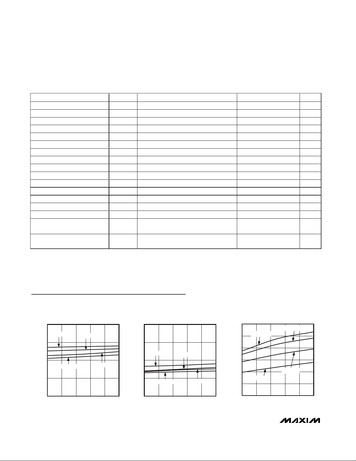
SUPPLY CURRENT vs. SUPPLY VOLTAGE
(INTERFACE IDLE, ALL OUTPUTS OFF,
R
SET
= 720Ω)
MAX6971 toc01
SUPPLY VOLTAGE (V)
SUPPLY CURRENT (mA)
5.04.53.5 4.0
1.85
1.90
1.95
2.00
1.80
3.0 5.5
TA = +125°C
TA = +85°C
TA = -40°C
TA = +25°C
SUPPLY CURRENT vs. SUPPLY VOLTAGE
(INTERFACE IDLE, ALL OUTPUTS OFF,
R
SET
= 360Ω)
MAX6971 toc02
SUPPLY VOLTAGE (V)
SUPPLY CURRENT (mA)
5.04.53.5 4.0
3.55
3.60
3.65
3.70
3.50
3.0 5.5
TA = +125°C
TA = +85°C
TA = -40°C
TA = +25°C
10
30
25
20
15
35
40
3.0 4.03.5 4.5 5.0 5.5
MAX6971 toc03
SUPPLY VOLTAGE (V)
SUPPLY CURRENT (mA)
SUPPLY CURRENT vs. SUPPLY VOLTAGE
(INTERFACE IDLE, ALL OUTPUTS ON, R
SET
= 720Ω)
TA = +125°C
TA = +85°C
TA = +25°C
TA = -40°C
SYMBOL
MIN TYP MAX
t
DR, tDF
CLK Rising to OUT_ Rising Delay
CLK Rising to OUT_ Falling Delay
OE Rising to OUT_ Rising Delay
OE Falling to OUT_ Falling Delay
Page 5

MAX6971
16-Port, 36V Constant-Current LED Driver
_______________________________________________________________________________________ 5
Typical Operating Characteristics (continued)
(TA = +25°C, unless otherwise noted.)
15
20
30
25
45
40
35
3.0 4.03.5 4.5 5.0 5.5
MAX6971 toc04
SUPPLY VOLTAGE (V)
SUPPLY CURRENT (mA)
SUPPLY CURRENT vs. SUPPLY VOLTAGE
(INTERFACE IDLE, ALL OUTPUTS ON, R
SET
= 360Ω)
TA = +125°C
TA = +85°C
TA = +25°C
TA = -40°C
0
10
5
20
15
25
30
01.01.50.5 2.0 2.5 3.0
PORT OUTPUT CURRENT vs. PORT OUTPUT
VOLTAGE (R
SET
= 720Ω, V+ = 3.3V)
MAX6971 toc05
PORT OUTPUT VOLTAGE (V)
PORT OUTPUT CURRENT (mA)
TA = +125°C
TA = +85°C
TA = +25°C
TA = -40°C
0
20
10
40
30
50
60
01.01.50.5 2.0 2.5 3.0
PORT OUTPUT CURRENT vs. PORT OUTPUT
VOLTAGE (R
SET
= 360Ω, V+ = 3.3V)
MAX6971 toc06
PORT OUTPUT VOLTAGE (V)
PORT OUTPUT CURRENT (mA)
TA = +125°C
TA = +85°C
TA = -40°C
TA = +25°C
0
10
5
20
15
25
30
01.01.50.5 2.0 2.5 3.0
PORT OUTPUT CURRENT vs. PORT OUTPUT
VOLTAGE (R
SET
= 720Ω, V+ = 5.0V)
MAX6971 toc07
PORT OUTPUT VOLTAGE (V)
PORT OUTPUT CURRENT (mA)
TA = +125°C
TA = +85°C
TA = +25°C
TA = -40°C
0
20
10
40
30
50
60
0 1.0 1.50.5 2.0 2.5 3.0
PORT OUTPUT CURRENT vs. PORT OUTPUT
VOLTAGE (R
SET
= 360Ω, V+ = 5.0V)
MAX6971 toc08
PORT OUTPUT VOLTAGE (V)
PORT OUTPUT CURRENT (mA)
TA = +125°C
TA = +85°C
TA = +25°C
TA = -40°C
25.0
24.5
24.0
23.5
23.0
3.0 4.0
3.5
4.5 5.0 5.5
PORT OUTPUT CURRENT vs. SUPPLY
VOLTAGE (R
SET
= 720Ω, V
OUT
= 2V)
MAX6971 toc09
SUPPLY VOLTAGE (V)
PORT OUTPUT CURRENT (mA)
TA = +25°C
TA = -40°C
TA = +85°C
TA = +125°C
49
48
47
46
3.0 4.0
3.5
4.5 5.0 5.5
PORT OUTPUT CURRENT vs. SUPPLY
VOLTAGE (R
SET
= 360Ω, V
OUT
= 2V)
MAX6971 toc10
SUPPLY VOLTAGE (V)
PORT OUTPUT CURRENT (mA)
TA = +125°C
TA = +85°C
TA = +25°C
TA = -40°C
0
10
30
20
40
50
021345
PORT OUTPUT CURRENT
vs. R
SET
RESISTANCE (V+ = 5.0V)
MAX6971 toc11
R
SET
RESISTANCE (kΩ)
PORT OUTPUT CURRENT (mA)
Page 6

MAX6971
16-Port, 36V Constant-Current LED Driver
6 _______________________________________________________________________________________
Pin Description
PIN NAME FUNCTION
1 GND Ground
2DIN Serial-Data Input. Data is loaded into the internal 16-bit shift register on CLK’s rising edge.
3 CLK Serial-Clock Input. Data is loaded into the internal 16-bit shift register on CLK’s rising edge.
4LE
Load - E nab l e Inp ut. D ata i s l oad ed tr ansp ar entl y f r om the i nter nal shi ft r eg i ster ( s) to the outp ut l atch( es)
w hi l e LE i s hi g h. D ata i s l atched i nto the outp ut l atch( es) on LE ’ s fal l i ng ed g e, and r etai ned w hi l e LE i s l ow .
5–20
LED Driver Outputs. OUT0 to OUT15 are open-drain, constant-current-sinking outputs rated to 28V.
21 OE
Output-Enable Input. High forces outputs OUT0 to OUT15 high impedance, without altering the contents
of the output latches. Low enables outputs OUT0 to OUT15 to follow the state of the output latches.
22 DOUT
Serial-Data Output. Data is clocked out of the 16-bit internal shift register to DOUT on CLK’s rising edge.
23 SET LED Current Setting. Connect SET to GND through a resistor (R
SET
) to set the maximum LED current.
24 V+ Positive Supply Voltage. Bypass V+ to GND with a 0.1µF ceramic capacitor.
Figure 1. Block Diagram
OUT0–OUT15
CLK
MAX6971
SERIAL-TO-PARALLEL SHIFT REGISTER
D0 D15
LE
OE
D0 D15
LATCHES
POWER-ON
RESET
V+
DOUTDIN
V+
D0 D15
OUT0
CONSTANT-CURRENT SINKS
OUT2
OUT1
OUT3
OUT4
OUT15
CURRENT
REFERENCE
GND GND
R
SET
Page 7

Detailed Description
The MAX6971 LED driver comprises a 4-wire serial
interface driving 16 constant-current-sinking, opendrain output ports. The outputs drive LEDs in either
static or multiplex applications (Figure 1). The constantcurrent outputs are guaranteed for current accuracy
not only with chip-supply voltage variations (5V ±10%
and 3V to 5.5V), but also over a realistic range of driver
output voltage drop (0.8V to 2.5V). The drivers use current-sensing feedback circuitry (not simple current mirrors) to ensure very small current variations over the full
allowed range of output voltage (see the Typical
Operating Characteristics).
The 4-wire serial interface comprises a 16-bit shift register and a 16-bit transparent latch. The shift register is
written through a clock input, CLK, and a data input,
DIN, and the data propagates to a data output, DOUT.
The data output allows multiple drivers to be cascaded
and operated together. The contents of the 16-bit shift
register are loaded into the transparent latch through a
latch-enable input, LE. The latch is transparent to the
shift register outputs when high, and latches the current
state on the falling edge of LE.
Each driver output is an open-drain, constant-current
sink that should be connected to the cathode of either
a single LED or a series string of multiple LEDs. The
LED anode can be connected to a supply voltage of up
to 36V, independent of the MAX6971 supply, V+. The
constant-current capability is up to 55mA per output,
set for all eight outputs by an external resistor, R
SET
.
4-Wire Serial Interface
The serial interface on the MAX6971 is a 4-wire serial
interface using four inputs (DIN, CLK, LE, OE) and a
data output (DOUT). This interface is used to write display data to the MAX6971. The serial-interface data
word length is 16 bits, D0–D15. See Figure 2.
The functions of the five interface pins are as follows.
DIN is the serial-data input, and must be stable when it
is sampled on the rising edge of CLK. Data is shifted in,
MSB first. This means that data bit D15 is clocked in
first, followed by 15 more data bits finishing with the
LSB, D0.
MAX6971
16-Port, 36V Constant-Current LED Driver
_______________________________________________________________________________________ 7
.
D15 D14
t
DS
t
DH
t
CL
t
CP
t
DO
t
OEW
t
OEL
t
f
t
r
t
OEH
t
LS
t
LW
t
CH
D1 D0
D7
LE
CLK
DIN
DOUT
OE
OUT_
80%
20%
t
LF
Figure 2. 4-Wire Serial-Interface Timing Diagram
Page 8

MAX6971
16-Port, 36V Constant-Current LED Driver
8 _______________________________________________________________________________________
CLK is the serial-clock input, which shifts data at DIN
into the MAX6971 16-bit shift register on its rising edge.
LE is the latch load input of the MAX6971 that transfers
data from the MAX6971 16-bit shift register to its 16-bit
latch when LE is high (transparent latch), and latches
the data on the falling edge of LE (Figure 2).
The fourth input provides output-enable control of the
output drivers. OE is high to force outputs
OUT0–OUT15 high impedance, without altering the
contents of the output latches, and low to enable outputs OUT0–OUT15 to follow the state of the output
latches.
OE is independent of the operation of the serial interface. Data can be shifted into the serial-interface shift
register and latched, regardless of the state of OE.
DOUT is the serial-data output, which shifts data out
from the MAX6971’s 16-bit shift register on the rising
edge of CLK. Data at DIN is propagated through the
shift register and appears at DOUT 16 clock cycles later.
LE
OUT_
LE
OUT_
CLK
OUT_
CLK
OUT_
t
CRR
t
CRF
t
LRR
t
LRF
Figure 3. LE and CLK to OUT_ Timing
Table 1. 4-Wire Serial-Interface Truth Table
SHIFT-REGISTER
CONTENTS
LATCH CONTENTS OUTPUT CONTENTS
SERIAL
DATA
INPUT
DIN
CLOCK
LOAD
BLANKING
OE
D
n
H
—
—
—
L
—
—
—
X
—
—
—
——
H
—
—
——
L
L
P
n
——
—
H
Hi-Z
L = Low-logic level.
H = High-logic level.
X = Don’t care.
P = Present state.
R = Previous state.
Hi-Z = High impedance.
INPUT
CLK
D
0D1D2
HR1R2…R
LR1R2…R
R0R1R2…R
XXX…XX
P1P2P3…P
——————
…D
n-1Dn
n-2Rn-1
n-2Rn-1
n-1Rn
n-1Pn
INPUT
LE
D
0D1D2
——————
——————
——————
R0R1R2—R
P0P1P2…P
XXX…XX
…D
n-1Dn
n-1Rn
n-1Pn
INPUT
D0D1D2…D
— ————
—————
—————
—————
P0P1P2… P
Hi-Z Hi-Z Hi-Z … Hi-Z
n-1
n-1
Page 9
Applications Information
Selecting External Component R
SET
to Set
LED Output Current
The MAX6971 uses an external resistor, R
SET
, to set the
LED current for outputs OUT0–OUT15. The minimum
allowed value of R
SET
is 327.3Ω, which sets the output
currents to 55mA. The maximum allowed value of R
SET
is 5kΩ. The reference value, 360Ω, sets the output cur-
rents to 50mA. To set a different output current, use the
formula:
R
SET
= 18,000 / I
OUT
where I
OUT
is the desired output current in mA.
Computing Power Dissipation
The upper limit for power dissipation (PD) for the
MAX6971 is determined by the following equation:
PD= (V+ x I+) + (V
OUT
x DUTY x I
OUT
x N)
where:
V+ = supply voltage
I+ = operating supply current when sinking I
OUT
LED
drive current into N outputs
DUTY = PWM duty cycle applied to OE
N = number of MAX6971 outputs driving LEDs at the
same time (maximum is 16)
V
OUT
= MAX6971 port output voltage when driving load
LED(s)
I
OUT
= LED drive current programmed by R
SET
PD= power dissipation, in mW if currents are in mA
Dissipation example:
I
OUT
= 20mA, N = 16, DUTY = 1, V
OUT
= 2V, V+ =
5.25V
P
D
= (5.25V x 25mA) + (2V x 1 x 20mA x 16) = 0.77W
Thus, for a 24-pin TSSOP package (T
JA
= 1 / 0.0122 =
+82°C/W from the Absolute Maximum Ratings), the
maximum allowed ambient temperature T
A
is given by:
T
J(MAX)
= TA+ (PDx TJA) = +150°C =
T
A
+ (0.77 x 82°C/W)
so TA= +86°C.
Overtemperature Cutoff
The MAX6971 contains an internal temperature sensor
that turns off all outputs when the die temperature
exceeds approximately +165°C. The outputs are
enabled again when the die temperature drops below
approximately +140°C. Register contents are not
affected, so when a driver is overdissipating, the external symptom is the load LEDs cycling between on and
off as the driver repeatedly overheats and cools, alternately turning the LEDs off and then back on again.
Power-Supply Considerations
The MAX6971 operates with a chip supply V+, and one
or more LED supplies. Bypass each supply to GND
with a 0.1µF capacitor as close to the MAX6971 as possible. This is normally adequate for static LED driving.
For multiplex or PWM applications, it is necessary to
add an additional bulk electrolytic capacitor of 4.7µF or
more to each supply for every 4 to 16 MAX6971s. The
necessary capacitance depends on the LED load current, PWM switching frequency, and serial-interface
speed. Inadequate V+ decoupling can cause timing
problems, and very noisy LED supplies can affect LED
current regulation.
Chip Information
PROCESS: BiCMOS
MAX6971
16-Port, 36V Constant-Current LED Driver
_______________________________________________________________________________________ 9
Page 10

MAX6971
16-Port, 36V Constant-Current LED Driver
10 ______________________________________________________________________________________
µC
MOSI
OUT0
OUT1
OUT2
OUT3
OUT4
OUT5
OUT6
OUT7
SCLK
DIN
CLK
0V
GND
MISO DOUT
0V
360Ω
OEENABLE
+5V
V+
+28V
LATCHLOAD
SET
MAX6971
OUT8
OUT9
OUT10
OUT11
OUT12
OUT13
OUT14
OUT15
Typical Application Circuit
Selector Guide
PART
NUMBER OF
OUTPUTS
MAX OUTPUT
VOLTAGE (V)
MAX OUTPUT
LED FAULT
DETECTION
WATCHDOG
MAX6968 ——
MAX6977 Yes —
MAX6978
8 5.5
Yes Yes
MAX6970* ——
MAX6981* Yes —
MAX6980*
836
Yes Yes
MAX6969 ——
MAX6979
16 5.5
Yes Yes
MAX6971 ——
MAX6983
16 36
Yes Yes
55
*Future product—contact factory for availability.
CURRENT (mA)
Page 11

MAX6971
16-Port, 36V Constant-Current LED Driver
______________________________________________________________________________________ 11
TSSOP4.40mm.EPS
PACKAGE OUTLINE, TSSOP 4.40mm BODY
21-0066
1
1
G
Package Information
(The package drawing(s) in this data sheet may not reflect the most current specifications. For the latest package outline information
go to www.maxim-ic.com/packages
.)
Page 12

MAX6971
16-Port, 36V Constant-Current LED Driver
Maxim cannot assume responsibility for use of any circuitry other than circuitry entirely embodied in a Maxim product. No circuit patent licenses are
implied. Maxim reserves the right to change the circuitry and specifications without notice at any time.
12 ____________________Maxim Integrated Products, 120 San Gabriel Drive, Sunnyvale, CA 94086 408-737-7600
© 2005 Maxim Integrated Products Printed USA is a registered trademark of Maxim Integrated Products, Inc.
Heaney
Package Information (continued)
(The package drawing(s) in this data sheet may not reflect the most current specifications. For the latest package outline information
go to www.maxim-ic.com/packages
.)
PDIPN.EPS
 Loading...