

Page 1
General Description
The MAX6958/MAX6959 compact multiplexed common-cathode display drivers interface microprocessors
to seven-segment numeric LED digits, or discrete LEDs
through an SMBus™- and I2C-compatible 2-wire serial
interface. The 2-wire serial interface uses fixed
0.8V/2.1V logic thresholds for compatibility with 2.5V
and 3.3V systems when the display driver is powered
from a 5V supply.
The MAX6958/MAX6959 drive up to four 7-segment
digits, with decimal points, plus four discrete LEDs, or
four 7-segment digits and eight discrete LEDs if the
digits’ decimal points are not used, or up to 36 discrete
LEDs. The MAX6959 also includes two input ports, one
or both of which may be configured as a key-switch
reader, which automatically scans and debounces a
matrix of up to eight switches. Key-switch status is
obtained by polling internal status registers or by configuring the MAX6959 interrupt output.
Other on-chip features include a hexadecimal font for
seven-segment displays, multiplex scan circuitry,
anode and cathode drivers, and static RAM that stores
each digit. The peak segment current for the display
digits is set internally to 23mA. Display intensity is
adjusted using a 64-step internal digital brightness control. The MAX6958/MAX6959 include a low-power shutdown mode, a scan-limit register that allows the user to
display from one to four digits, and a test mode, which
forces all LEDs on. The LED drivers are slew-rate-limited to reduce EMI.
The MAX6958/MAX6959 are available in 16-pin PDIP
and QSOP packages and are fully specified over the
-40°C to +125°C automotive temperature range.
Applications
Features
♦ 400kbps 2-Wire Serial Interface
♦ 3V to 5.5V Operation
♦ Drive 4 Digits plus 4 or 8 Discrete LEDs
♦ Drive Common-Cathode LED Digits
♦ 23mA Constant-Current LED Segment Drive
♦ Hexadecimal Decode/No-Decode Digit Selection
♦ 64-Step Digital Brightness Control
♦ Slew-Rate-Limited Segment Drivers Reduced EMI
♦ Debounces Up to Eight Switches with n-Key
Rollover (MAX6959 Only)
♦ IRQ Output When a Key Input Is Debounced
(MAX6959 Only)
♦ 20µA Low-Power Shutdown (Data Retained)
♦ Automotive Temperature Range (-40°C to +125°C)
♦ Compact 16-Pin PDIP and QSOP Packages
MAX6958/MAX6959
2-Wire Interfaced, 3V to 5.5V, 4-Digit,
9-Segment LED Display Drivers with Keyscan
________________________________________________________________ Maxim Integrated Products 1
Ordering Information
19-2634; Rev 0; 10/02
For pricing, delivery, and ordering information, please contact Maxim/Dallas Direct! at
1-888-629-4642, or visit Maxim’s website at www.maxim-ic.com.
Ordering Information continued at end of data sheet.
*EP = Exposed pad.
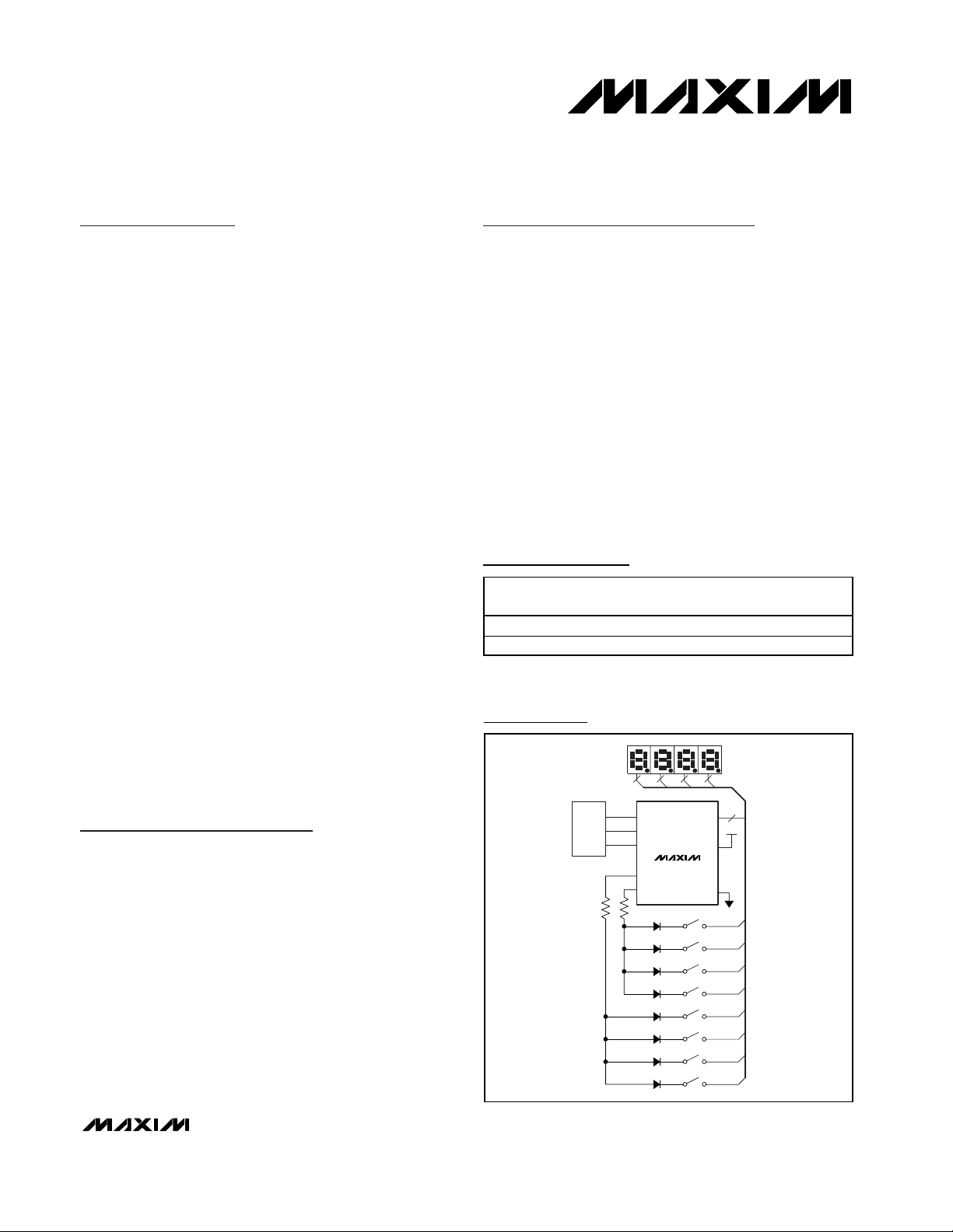
Typical Operating Circuit
SMBus is a trademark of Intel Corp.
Set-Top Boxes
Panel Meters
White Goods
Audio/Video Equipment
Vending Machines
Industrial Controls
Pin Configuration, Functional Diagram, and Typical
Application Circuit appear at end of data sheet.
PART
TEMP
RANGE
MAX6958AAEE -40°C to +125°C 0111000 16 QS O P - E P *
MAX6958AAPE -40°C to +125°C 0111000 16 DIP
SLAVE
ADDRESS
PINPACKAGE
8 88 8
µC
SDA
SCL
SDA
SCL
IRQ
IRQ/SEG9
MAX6959
INPUT1
INPUT2
DIG0–DIG3
SEG0–SEG8
Key0
Key1
Key2
Key3
Key4
Key5
Key6
Key7
8
5V
V+
GND
DIG0/SEG0
DIG1/SEG1
DIG2/SEG2
DIG3/SEG3
DIG4/SEG4
DIG5/SEG5
DIG6/SEG6
DIG7/SEG7
Page 2
MAX6958/MAX6959
2-Wire Interfaced, 3V to 5.5V, 4-Digit,
9-Segment LED Display Drivers with Keyscan
2 _______________________________________________________________________________________
ABSOLUTE MAXIMUM RATINGS
DC ELECTRICAL CHARACTERISTICS
(V+ = 3V to 5.5V, TA= T
MIN
to T
MAX
, unless otherwise noted. Typical values are at V+ = 5V, TA= +25°C.) (Note 1)
Stresses beyond those listed under “Absolute Maximum Ratings” may cause permanent damage to the device. These are stress ratings only, and functional
operation of the device at these or any other conditions beyond those indicated in the operational sections of the specifications is not implied. Exposure to
absolute maximum rating conditions for extended periods may affect device reliability.
Voltage (with respect to GND)
V+, SCL, SDA .......................................................-0.3V to +6V
All Other Pins............................................-0.3V to (V+ + 0.3V)
Current
DIG0/SEG0–DIG3/SEG3 Sink Current ..........................275mA
DIG0/SEG0–SEG9 Source Current .................................30mA
SCL, SDA, INPUT1, INPUT2 ...........................................20mA
Continuous Power Dissipation (TA= +70°C)
16-Pin DIP (derate at 10.5mW/°C above +70°C).........842mW
16-Pin QSOP (derate at 8.34mW/°C above +70°C).....667mW
Operating Temperature Range
MAX695_ (T
MIN
to T
MAX
) ...............................-40°C to +125°C
Junction Temperature......................................................+150°C
Storage Temperature Range .............................-65°C to +150°C
Lead Temperature (soldering, 10s) .................................+300°C
PARAMETER SYMBOL CONDITIONS MIN TYP MAX UNITS
Operating Supply Voltage V+ 3 5.5 V
Shutdown Supply Current I
Operating Supply Current I+
Display Scan Rate f
Keyscan Debounce Time t
Segment Drive Source Current I
Segment Current Slew Rate ∆I
Segment Drive Current Matching ∆I
LOGIC INPUTS AND OUTPUTS
Input Leakage Current SCL
and SDA
Logic High Input Voltage SCL,
SDA
Logic Low Input Voltage SCL,
SDA
Input Leakage Current INPUT1,
INPUT2
Logic High Input Voltage INPUT1,
INPUT2
Logic Low Input Voltage INPUT1,
INPUT2
SHDN
Shutdown mode, all
digital inputs at V+
Intensity set to full,
no display load
connected, INPUT1
and INPUT2 open
circuit
SCAN
DEBOUNCE
4 digits scanned TA = T
V
= 2.4V,
LED
V+ = 4.5V to 5.5V
SEG
V
LED
= 2V,
V+ = 3V to 5.5V
/∆t 11 mA/µs
SEG
SEG
, I
I
IH
IL
V
IH
V
IL
I
, I
INH
V
INH
V
INL
INPUT_ = V+ -1 +1 µA
INL
TA = +25°C2050
= T
T
A
to +85°C 125
MIN
TA = +25°C 5.9 6.7
T
= T
A
TA = T
MIN
MIN
MIN
to T
to T
to T
MAX
MAX
MAX
510 780 1050 Hz
30.3 41 63 ms
7.5
TA = +25°C -19 -23 -29
T
= T
MIN
to T
MAX
A
-18 -30
TA = +25°C -16 -29.5
T
= T
MIN
to T
MAX
A
-15.5 -30.5
4%
-1 +1 µA
2.1 V
0.8 V
0.7 ✕
V+
0.3 ✕
V+
µA
mA
mA
V
V
Page 3
MAX6958/MAX6959
2-Wire Interfaced, 3V to 5.5V, 4-Digit,
9-Segment LED Display Drivers with Keyscan
_______________________________________________________________________________________ 3
Note 1: All parameters tested at TA=+25°C. Specifications over temperature are guaranteed by design.
Note 2: Guaranteed by design.
Note 3: A master device must provide a hold time of at least 300ns for the SDA signal (referred to V
IL
of the SCL signal) in order to
bridge the undefined region of SCL’s falling edge.
Note 4: C
B
= total capacitance of one bus line in pF. tRand tFmeasured between 0.3V+ and 0.7V+.
Note 5: I
SINK
≤ 6mA. CB= total capacitance of one bus line in pF. tRand tFmeasured between 0.3V+ and 0.7V+.
Note 6: Input filters on the SDA and SCL inputs suppress noise spikes less than 50ns.
DC ELECTRICAL CHARACTERISTICS (continued)
(V+ = 3V to 5.5V, TA= T
MIN
to T
MAX
, unless otherwise noted. Typical values are at V+ = 5V, TA= +25°C.) (Note 1)
)
TIMING CHARACTERISTICS
(V+ = 3V to 5.5V, TA= T
MIN
to T
MAX
, Figure 1, unless otherwise noted.) (Note 1)
Pullup to V+ INPUT1, INPUT2 I
IRQ/SEG9, SDA Output Low
Voltage
SDA Output Low Voltage V
PARAMETER SYMBOL CONDITIONS MIN TYP MAX UNITS
PULLUP
I
= 6mA, TA = -40°C to +85°C 0.4
V
OLBK
OL(SDA
SINK
I
= 4mA, TA = T
SINK
I
= 6mA 0.4 V
SINK
MIN
to T
Serial Clock Frequency f
Bus Free Time Between a STOP
and a START Condition
Hold Time (Repeated) START
Condition
Repeated START Setup Time t
STOP Condition Setup Time t
Data Hold Time t
Data Setup Time t
SCL Clock Low Period t
SCL Clock High Period t
Rise Time of Both SDA and SCL
Signals, Receiving
Fall Time of Both SDA and SCL
Signals, Receiving
Fall Time of SDA Transmitting t
Pulse Width of Spike Suppressed t
Capacitive Load for Each Bus
Line
PARAMETER SYMBOL CONDITIONS MIN TYP MAX UNITS
SCL
t
BUF
t
HD, STA
SU, STA
SU, STO
HD, DAT
SU, DAT
LOW
HIGH
t
t
SP
C
(Note 3) 0.9 µs
(Notes 2, 4)
R
(Notes 2, 4)
F
(Notes 2, 5)
F
(Note 6) 50 ns
B
MAX
26.5 µA
0.4
400 kHz
1.3 µs
0.6 µs
0.6 µs
0.6 µs
100 ns
1.3 µs
0.6 µs
20 +
0.1C
20 +
0.1C
20 +
0.1C
400 pF
B
B
B
300 ns
300 ns
250 ns
V
Page 4
MAX6958/MAX6959
2-Wire Interfaced, 3V to 5.5V, 4-Digit,
9-Segment LED Display Drivers with Keyscan
4 _______________________________________________________________________________________
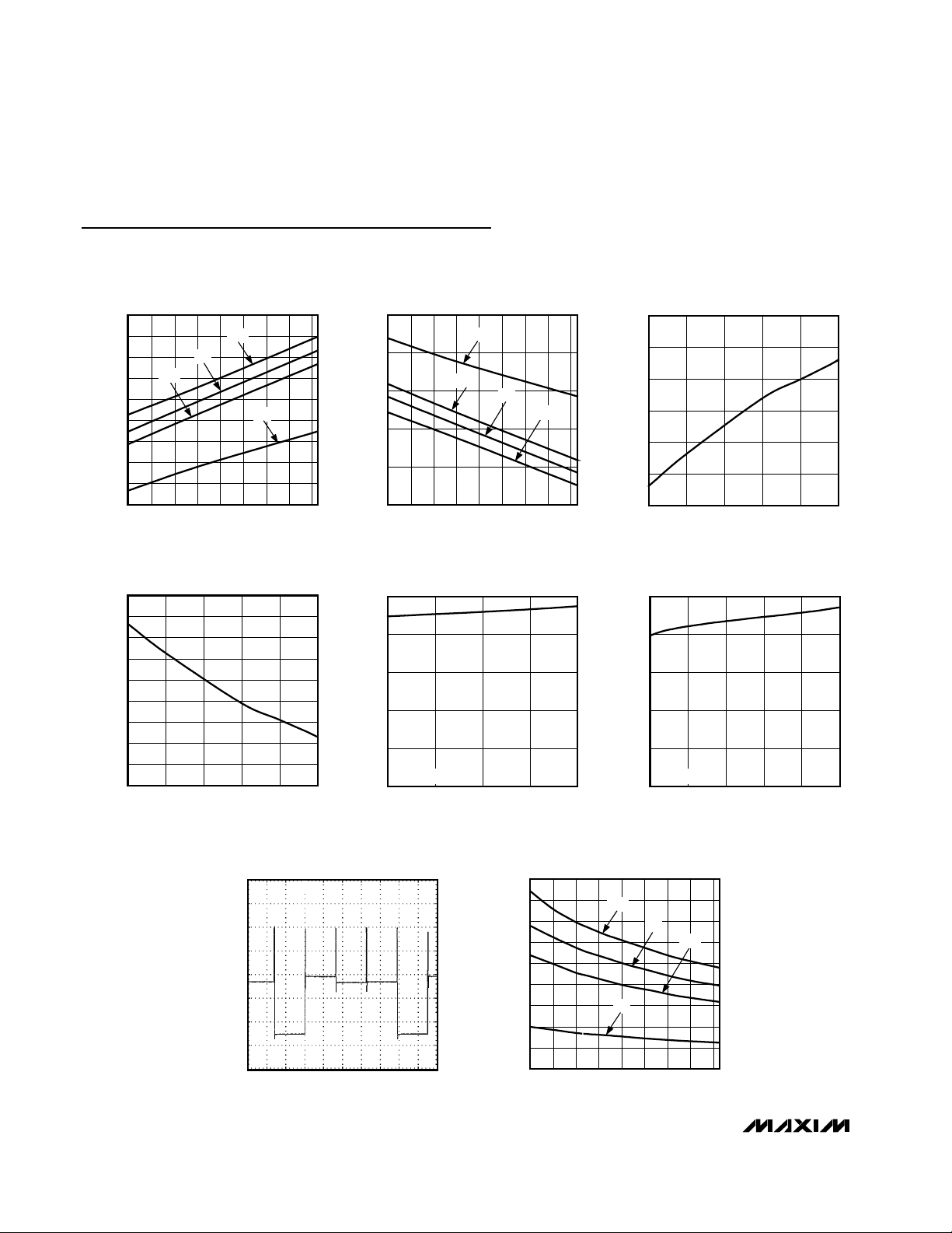
Typical Operating Characteristics
(V+ = 5V, LED forward voltage = 2.4V, TA= +25°C, unless otherwise noted.)
SCAN RATE (f
SCAN
)
vs. TEMPERATURE
MAX6958/59 toc01
TEMPERATURE (°C)
SCAN RATE (Hz)
1008040 600 20-20
760
765
770
775
780
785
790
795
800
755
-40 120
5.5V
5V
3V
4.5V
KEYSCAN DEBOUNCE TIME (t
DEBOUNCE
)
vs. TEMPERATURE
MAX6958/59 toc02
TEMPERATURE (°C)
KEYSCAN DEBOUNCE TIME (ms)
100806040200-20
40.5
41.0
41.5
42.0
42.5
40.0
-40 120
4.5V
5V
3V
5.5V
SCAN RATE (f
SCAN
)
vs. SUPPLY VOLTAGE
MAX6958/59 toc03
SUPPLY VOLTAGE (V)
SCAN RATE (Hz)
5.04.54.03.5
765
770
775
780
785
790
760
3.0 5.5
KEYSCAN DEBOUNCE TIME (t
DEBOUNCE
)
vs. SUPPLY VOLTAGE
MAX6958/59 toc04
SUPPLY VOLTAGE (V)
KEYSCAN DEBOUNCE TIME (ms)
5.04.54.03.5
40.6
40.8
41.0
41.2
41.4
41.6
41.8
42.0
42.2
40.4
3.0 5.5
SEGMENT SOURCE CURRENT
vs. SUPPLY VOLTAGE
MAX6958/59 toc05
SUPPLY VOLTAGE (V)
SEGMENT SOURCE CURRENT (mA)
5.255.004.75
5
10
15
20
25
0
4.50 5.50
V
LED
= 2.4V
SEGMENT SOURCE CURRENT
vs. SUPPLY VOLTAGE
MAX6958/59 toc06
SUPPLY VOLTAGE (V)
SEGMENT SOURCE CURRENT (mA)
4.54.03.5
5
10
15
20
25
0
3.0 5.0 5.5
V
LED
= 2V
WAVEFORM AT DIG0/SEG0,
FULL INTENSITY
MAX6958/59 toc07
V
DIG0
/
SEG0
1V/div
200µs/div
INPUT PULLUP CURRENT
vs. TEMPERATURE
MAX6958/59 toc08
TEMPERATURE (°C)
INPUT PULLUP CURRENT (µA)
1008040 600 20-20
5
10
15
20
25
30
35
40
45
0
-40 120
5.5V
5V
3V
4.5V
Page 5
Detailed Description
The MAX6958/MAX6959 serially interfaced display drivers drive up to: four 7-segment digits plus four discrete LEDs if the decimal points are used, or four
7-segment digits plus eight discrete LEDs if the decimal points are not used, or 36 discrete LEDs. Table 1
lists the display connection scheme.
The MAX6958/MAX6959 include the hexadecimal font
map for seven-segment displays. The seven-segment
LED digits can be controlled directly or programmed to
use the hexadecimal font. Direct segment control
allows the MAX6958/MAX6959 to drive bar graphs and
discrete LED indicators.
The MAX6958/MAX6959 use a multiplexing scheme that
minimizes the connections between the driver and LED
display. The MAX6958/MAX6959 can drive monocolor
and bicolor single-digit type displays, and monocolor
dual-digit displays. Dual-digit displays internally
wire together the equivalent segments for each digit,
requiring only eight segment pins instead of 16. The
MAX6958/MAX6959 can also drive multidigit LED displays that have the segments individually pinned for
each digit.
To connect four single-digit displays to the MAX6958/
MAX6959, connect cathode outputs DIG0/SEG0–
DIG3/SEG3 to the cathodes of the four display digits as
shown in Table 1 (CC0–CC3). Drive eight additional
LEDs with SEG0 to SEG7. Four of the eight LEDs can
be the decimal point (DP) segments of the four displays, and the other four can be discrete LED indicators.
To connect two dual-digit displays to the MAX6958/
MAX6959, connect cathode outputs DIG0/SEG0 and
DIG1/SEG1 to the cathodes of the first dual digit.
Connect DIG2/SEG2 and DIG3/SEG3 to the cathodes
of the second dual digit. SEG0 to SEG3 can only drive
discrete LEDs, not digit DP segments. SEG4 to SEG7
can drive the DP segments if required. Bicolor singledigit displays are connected and treated as dual-digit
displays, each digit being one of the two colors.
MAX6958/MAX6959
2-Wire Interfaced, 3V to 5.5V, 4-Digit,
9-Segment LED Display Drivers with Keyscan
_______________________________________________________________________________________ 5
Pin Description
Table 1. Standard Driver Connection to LED Displays
PIN
MAX6958 MAX6959
1 1 SDA Serial Data I/O
2 2 SCL Serial Clock Input
3 — SEG9 Segment Output. Segment driver sourcing current to a display anode.
— 3 IRQ/SEG9
4–7, 11–15 4–7, 11–15 DIGX, SEGX
8 8 GND Ground
9, 10 — N.C. No Connect. Connect to V+ or leave open.
— 9 INPUT1
— 10 INPUT2
16 16 V+ Positive Supply Voltage
NAME FUNCTION
Interrupt or Segment Output. May be segment driver sourcing current to a display
anode, or open-drain interrupt output, or open-drain logic output.
Digit and Segment Drivers. Digit X outputs sink current from the display common
cathode when acting as digit drivers. Segment X drivers source current to the display
anodes. Segment/digit drivers are high impedance when turned off.
General-Purpose Input Port 1 with Internal Pullup. May be configured as generalpurpose logic input or keyscan input. Connect to V+ or leave open if unused.
General-Purpose Input Port 2 with Internal Pullup. May be configured as generalpurpose logic input or keyscan input. Connect to V+ or leave open if unused.
LED Digit 0 CC0 SEG 0 SEG g SEG f SEG e SEG d SEG c SEG b SEG a SEG 4
LED Digit 1 SEG 1 CC1 SEG g SEG f SEG e SEG d SEG c SEG b SEG a SEG 5
LED Digit 2 SEG g SEG f CC2 SEG 2 SEG e SEG d SEG c SEG b SEG a SEG 6
LED Digit 3 SEG g SEG f SEG 3 CC3 SEG e SEG d SEG c SEG b SEG a SEG 7
DIG0/SEG0 DIG1/SEG1 DIG2/SEG2 DIG3/SEG3 SEG 4 SEG 5 SEG 6 SEG 7 SEG 8 SEG 9/IRQ
Page 6
MAX6958/MAX6959
Differences Between MAX6958
and MAX6959
The MAX6958/MAX6959 have the same LED drive
capability, four common-cathode digits of nine segments per digit. The MAX6959 additionally contains two
logic input ports, INPUT1 and INPUT2. Each input port
can be individually configured as either a general-purpose input port that is read through the serial interface,
or as a keyscan input. In keyscan mode, the input is
used to read and automatically debounce four key
switches. A maximum of eight key switches can be
read if both INPUT1 and INPUT2 are assigned to
keyscanning.
The MAX6958's SEG9 output is preconfigured as the
9th LED segment output. The IRQ/SEG9 output on the
MAX6959 can be configured as either an open-drain
logic output or the 9th segment output. This logic output serves as either a general-purpose logic output, set
through the serial interface, or an interrupt (IRQ) output
that alerts a microcontroller of debounced key-switch
events. Key-switch status can also be obtained by
polling the internal status registers at any time.
Use the Option bit in the configuration register to detect
whether a MAX6958 or MAX6959 is present. The option
bit allows host software to establish whether a high-end
front panel (using the MAX6959 for keyscan support) or
a low-end panel (using a MAX6958 and no key switches) is fitted to a product.
Serial Interface
Serial Addressing
The MAX6958/MAX6959 operate as a slave that sends
and receives data through a 2-wire interface. The interface uses a serial data line (SDA) and a serial clock line
(SCL) to achieve bidirectional communication between
master(s) and slave(s). A master, typically a microcontroller, initiates all data transfers to and from the
MAX6958/MAX6959, and generates the SCL clock that
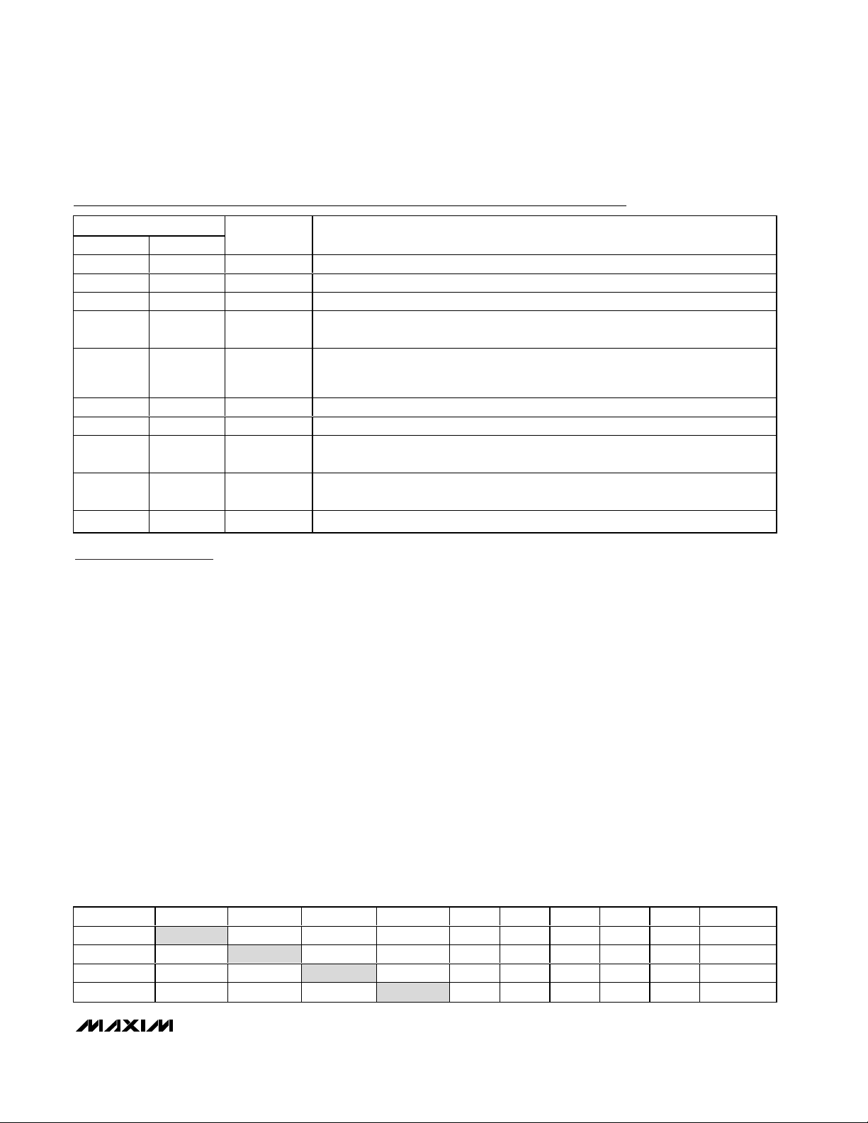
synchronizes the data transfer (Figure 1).
The MAX6958/MAX6959 SDA line operates as both an
input and an open-drain output. A pullup resistor, typically 4.7kΩ, is required on the SDA bus. The MAX6958/
MAX6959 SCL line operates only as an input. A pullup
resistor, typically 4.7kΩ, is required on the SCL bus if
there are multiple masters on the 2-wire interface, or if
the master in a single-master system has an open-drain
SCL output.
Each transmission consists of a START condition
(Figure 2) sent by a master, followed by the MAX6958/
MAX6959 7-bit slave address plus R/W bit (Figure 3), 1
or more data bytes, and finally a STOP condition
(Figure 2).
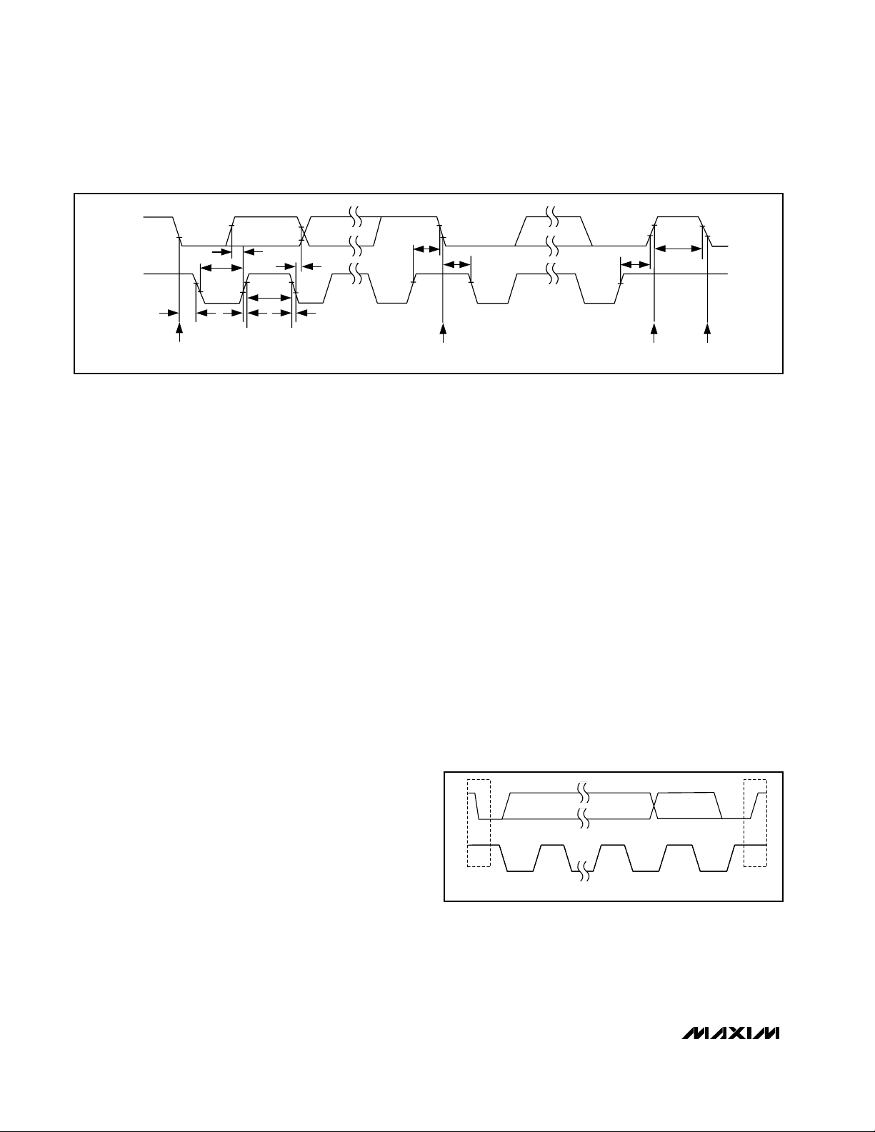
Start and Stop Conditions
Both SCL and SDA remain high when the interface is
not busy. A master signals the beginning of a transmission with a START (S) condition by transitioning SDA
from high to low while SCL is high. When the master
has finished communicating with the slave, it issues a
STOP (P) condition by transitioning the SDA from low to
high while SCL is high. The bus is then free for another
transmission (Figure 2).
2-Wire Interfaced, 3V to 5.5V, 4-Digit,
9-Segment LED Display Drivers with Keyscan
6 _______________________________________________________________________________________
Figure 1. 2-Wire Serial Interface Timing Details
Figure 2. Start and Stop Conditions
SDA
t
SU, DAT
t
t
LOW
LOW
SCL
t
HD, STA
START
CONDITION
t
HIGH
t
R
t
HD, DAT
t
F
t
SU, STA
t
BUF
REPEATED START
CONDITION
t
HD, STA
t
SU, STO
STOP
CONDITION
START
CONDITION
SDA
SCL
S
START
CONDITION
P
STOP
CONDITION
Page 7

Bit Transfer
One data bit is transferred during each clock pulse.
The data on the SDA line must remain stable while SCL
is high (Figure 4).
Acknowledge
The acknowledge bit is a clocked 9th bit that the recipient uses to handshake receipt of each byte of data
(Figure 5). Thus, each byte transferred effectively
requires 9 bits. The master generates the 9th clock
pulse, and the recipient pulls down SDA during the
acknowledge clock pulse, such that the SDA line is stable low during the high period of the clock pulse. When
the master is transmitting to the MAX6958/MAX6959,
the MAX6958/MAX6959 generate the acknowledge bit
because the MAX6958/MAX6959 are the recipients.
When the MAX6958/MAX6959 are transmitting to the
master, the master generates the acknowledge bit
because the master is the recipient.
Slave Address
The MAX6958/MAX6959 have a 7-bit-long slave
address (Figure 3). The eighth bit following the 7-bit
slave address is the R/W bit. Set the R/W bit low for a
write command and high for a read command.
The MAX6958/MAX6959 are available in one of two
possible slave addresses (see Table 2 and Ordering
Information). The first 6 bits (MSBs) of the MAX6958/
MAX6959 slave address are always 011100. Slave
address bit A0 is internally hardwired to either GND in
the MAX695_A_, or V+ in the MAX695_B_. A maximum
of two MAX6958/MAX6959 devices can share a bus.
Message Format for Writing
A write to the MAX6958/MAX6959 comprises the transmission of the MAX6958/MAX6959s’ slave address with
the R/W bit set to zero, followed by at least 1 byte of
information. The first byte of information is the command byte, which determines the register that stores
the next byte written to the MAX6958/MAX6959. If a
STOP condition is detected after the command byte is
received, the MAX6958/MAX6959 take no further action
(Figure 6) beyond storing the command byte.
MAX6958/MAX6959
2-Wire Interfaced, 3V to 5.5V, 4-Digit,
9-Segment LED Display Drivers with Keyscan
_______________________________________________________________________________________ 7
Figure 3. Slave Address
Figure 4. Bit Transfer
Figure 5. Acknowledge
Table 2. MAX6958/MAX6959 Address Map
Figure 6. Command Byte Received
SDA
SCL
SDA
SCL
01
MSB LSB
DATA STABLE,
DATA VALID
CHANGE OF
DATA ALLOWED
A0
START
CONDITION
SCL
SDA
1
R/W ACK11 00
CLOCK PULSE FOR
ACKNOWLEDGMENT
289
NOT ACKNOWLEDGE
ACKNOWLEDGE
COMMAND BYTE IS STORED ON RECEIPT OF STOP CONDITION
ACKNOWLEDGE FROM
MAX6958/MAX6959
S A0SLAVE ADDRESS COMMAND BYTE
R/W
AP
SLAVE ADDRESS
BIT A0
MAX695_A_ 0111000
MAX695_B_ 0111001
D15 D14 D13 D12 D11 D10 D9 D8
MAX6958/MAX6959 DEVICE ADDRESS
A6 A5 A4 A3 A2 A1 A0
ACKNOWLEDGE FROM
MAX6958/MAX6959
Page 8

MAX6958/MAX6959
Bytes received after the command byte are data bytes.
The first data byte goes into the internal register of the
MAX6958/MAX6959 as selected by the command byte
(Figure 7).
The address pointer in the MAX6958/MAX6959 autoincrements after each data byte. If multiple data bytes
are transmitted before a STOP condition is detected,
these bytes are stored in subsequent MAX6958/
MAX6959 internal registers (Figure 8), unless the
address pointer has reached address 01111111. The
address pointer does not autoincrement once address
01111111 has been reached (Table 3).
Message Format for Reading
The MAX6958/MAX6959 are read using the internally
stored command byte as an address pointer the same
way the stored command byte is used as an address
pointer for a write. The pointer autoincrements after
each data byte read using the same rules as for a write
(Table 3). A read is initiated by first configuring the
MAX6958/MAX6959s’ command byte with a write command (Figure 6). The master can now read n consecutive bytes from the MAX6958/MAX6959. The master
acknowledges receipt of each read byte during the
acknowledge clock pulse. The master must acknowledge all consecutive bytes received except the last
byte. The final read byte must be followed by a not
acknowledge from the master and then a stop condition (Figure 9). The first data byte is read from the register addressed by the initialized command byte
(Figure 8). Reset the address pointer when performing
read-after-write verification because the stored byte
address is autoincremented after the write. The
address pointer does not autoincrement if it points to
register 01111111 (Table 3).
Table 4 is the register address map.
2-Wire Interfaced, 3V to 5.5V, 4-Digit,
9-Segment LED Display Drivers with Keyscan
8 _______________________________________________________________________________________
Figure 7. Command and Single Data Byte Received
Figure 8. n Data Bytes Received
Figure 9. Reading n Data Bytes from the MAX6958/MAX6959
HOW CONTROL BYTE AND DATA BYTE MAP INTO
S AA
MAX6958/MAX6959s' REGISTERS
ACKNOWLEDGE FROM
MAX6958/MAX6959
R/W
D15 D14 D13 D12 D11 D10 D9 D8 D1 D0D3 D2D5 D4D7 D6
0SLAVE ADDRESS COMMAND BYTE DATA BYTE
HOW CONTROL BYTE AND DATA BYTE MAP INTO
S AA
MAX6958/MAX6959s' REGISTERS
ACKNOWLEDGE FROM
MAX6958/MAX6959
R/W
D15 D14 D13 D12 D11 D10 D9 D8 D1 D0D3 D2D5 D4D7 D6
0SLAVE ADDRESS COMMAND BYTE DATA BYTE
HOW THE MAX6958/MAX6959 SENDS DATA
ACKNOWLEDGE FROM MAX6958/MAX6959
TO THE MASTER
D15 D14 D13 D12 D11 D10 D9 D8 D1 D0D3 D2D5 D4D7 D6
ACKNOWLEDGE FROM MAX6958/MAX6959
ACKNOWLEDGE FROM MAX6958/MAX6959
ACKNOWLEDGE FROM THE MASTER
ACKNOWLEDGE FROM MAX6958/MAX6959
1 BYTE
AUTOINCREMENT MEMORY WORD ADDRESS
ACKNOWLEDGE FROM MAX6958/MAX6959
n BYTES
AUTOINCREMENT MEMORY WORD ADDRESS
NOT ACKNOWLEDGE FROM MASTER
P
A
P
A
S AA
1SLAVE ADDRESS FIRST DATA BYTE DATA BYTE
R/W
A
n BYTES
AUTOINCREMENT MEMORY WORD ADDRESS
AUTOINCREMENT MEMORY WORD ADDRESS
P
Page 9

Operation with Multiple Masters
If the MAX6958/MAX6959 are operated on a 2-wire
interface with multiple masters, a master reading the
MAX6958/MAX6959 should use a repeated start
between the write, which sets the MAX6958/MAX6959s’
address pointer, and the read(s) that takes the data
from the location(s) set by the address pointer. It is
possible for master 2 to take over the bus after master
1 has set up the MAX6958/MAX6959s’ address pointer
but before master 1 has read the data. If master 2 subsequently changes the MAX6958/MAX6959s’ address
pointer, then master 1's delayed read may be from an
unexpected location.
Command Address Autoincrementing
Address autoincrementing allows the MAX6958/
MAX6959 to be configured with the shortest number of
transmissions by minimizing the number of times the
command byte needs to be sent. The address pointer
stored in the MAX6958/MAX6959 increments after each
data byte is written or read, unless the address equals
01111111 (Table 3).
Digit Type Registers
The MAX6958/MAX6959 store display data in five registers. The four digit registers each control the seven
numeric segments of a seven-segment digit, but not
the DP segments. The segments register controls eight
individual LEDs, which can be any mix of discrete LEDs
and any or all of the DP segments of the four 7-segment digits (Table 5) (Figure 10).
MAX6958/MAX6959
2-Wire Interfaced, 3V to 5.5V, 4-Digit,
9-Segment LED Display Drivers with Keyscan
_______________________________________________________________________________________ 9
Table 3. Command Address
Autoincrement Behavior
Table 4. Register Address Map
Figure 10. Segment Labeling for 7-Segment Display
COMMAND BYTE
ADDRESS RANGE
00000000 to
01111110
01111111
AUTOINCREMENT BEHAVIOR
Command byte address autoincrements
after byte read or written
Command byte address remains at
01111111 after byte written or read
a
b
f
g
c
e
dp
d
REGISTER
No-op 0 0 0 0 0 0 0 0 0x00
Decode mode 0 0 0 0 0 0 0 1 0x01
Intensity 0 0 0 0 0 0 1 0 0x02
Scan limit 0 0 0 0 0 0 1 1 0x03
Configuration 0 0 0 0 0 1 0 0 0x04
Factory reserved. Do not write to this register. 0 0 0 0 0 1 0 1 0x05
GPIO (MAX6959 only) 0 0 0 0 0 1 1 0 0x06
Display test 0 0 0 0 0 1 1 1 0x07
Read key debounced (MAX6959 only)
A write to this register is ignored.
Read key pressed (MAX6959 only)
A write to this register is ignored.
Digit 0 0 0 1 0 0 0 0 0 0x20
Digit 1 0 0 1 0 0 0 0 1 0x21
Digit 2 0 0 1 0 0 0 1 0 0x22
Digit 3 0 0 1 0 0 0 1 1 0x23
Segments 0 0 1 0 0 1 0 0 0x24
D15 D14 D13 D12 D11 D10 D9 D8
0 0 0 0 1 0 0 0 0x08
0 0 0 0 1 1 0 0 0x0C
COMMAND ADDRESS
HEX
CODE
Page 10

MAX6958/MAX6959
The digit registers and segments register use 1 bit to
set the state of one segment. Each bit is high to turn a
segment on, or low to turn it off (Table 6).
Decode-Mode Register
The decode-mode register sets hexadecimal code
(0–9, A–F) or no-decode operation for each digit. Each
bit in the register corresponds to one digit. Logic high
selects hexadecimal decoding while logic low bypasses the decoder. Digits can be set for decode or no
decode in any combination. Bit assignment and examples of the decode mode control register format are
shown in Table 7.
In hexadecimal code-decode mode, the decoder looks
only at the lower nibble of the data in the digit register
(D3–D0), disregarding bits D7–D4. Table 7 lists the hexadecimal code font. When no decode is selected, data
bits D7–D0 correspond to the segment lines of the
MAX6958/MAX6959. Table 8 shows the one-to-one pairing of each data bit to the appropriate segment line.
Initial Power-Up
On initial power-up, all control registers are reset, the
display is blanked, and the MAX6958/MAX6959 enter
shutdown mode (Table 9). At power-up, the MAX6958/
MAX6959 are initially set to scan four digits, do not
decode data in the digit registers or scan key switches
(MAX6959 only), and the intensity register is set to a
low value (4/64 intensity).
2-Wire Interfaced, 3V to 5.5V, 4-Digit,
9-Segment LED Display Drivers with Keyscan
10 ______________________________________________________________________________________
Table 5. No-Decode Mode Data Bits and Corresponding Segment Lines
Table 6. No-Decode Mode Data Bits and
Corresponding Segment Lines
Table 7. Decode-Mode Register Examples
DIGIT/SEGMENT REGISTER
Digit 0 0x20 X SEG a SEG b SEG c SEG d SEG e SEG f SEG g
Digit 1 0x21 X SEG a SEG b SEG c SEG d SEG e SEG f SEG g
Digit 2 0x22 X SEG a SEG b SEG c SEG d SEG e SEG f SEG g
Digit 3 0x23 X SEG a SEG b SEG c SEG d SEG e SEG f SEG g
Segments 0x24 SEG 7 SEG 6 SEG 5 SEG 4 SEG 3 SEG 2 SEG 1 SEG 0
ADDRESS
CODE (HEX)
D7 D6 D5 D4 D3 D2 D1 D0
REGISTER DATA
REGISTER BIT SEGMENT BEHAVIOR
0 Segment off
1 Segment on
DECODE MODE
Bit assignment for each digit 0x01 XXXXDigit 3 Digit 2 Digit 1 Digit 0 —
No decode for digits 3–0 0x01 XXXX00000xX0
Hexadecimal decode for digit
0; no decode for digits 3–1
———————————
Hexadecimal decode for digits
2–0; no decode for digit 3
Hexadecimal decode for digit
3; no decode for digits 2–0
———————————
Hexadecimal decode for digits
3–0
ADDRESS
CODE (HEX)
0x01 XXXX0 0010xX1
0x01 XXXX0 1110xX7
0x01 XXXX1 0000xX8
0x01 XXXX1 1110xXF
D7 D6 D5 D4 D3 D2 D1 D0
REGISTER DATA
HEX
CODE
Page 11

MAX6958/MAX6959
2-Wire Interfaced, 3V to 5.5V, 4-Digit,
9-Segment LED Display Drivers with Keyscan
______________________________________________________________________________________ 11
Table 8. Seven-Segment Mapping Decoder for Hexadecimal Font
Table 9. Initial Power-Up Register Status
*MAX6959 only.
7-SEGMENT
CHARACTER
0 X00001111110
1 X00010110000
2 X00101101101
3 X00111111001
4 X01000110011
5 X01011011011
6 X01101011111
7 X01111110000
8 X10001111111
9 X10011111011
A X10101110111
B X10110011111
C X11001001110
D X11010111101
E X11101001111
F X11111000111
D7–D4 D3 D2 D1 D0 a b c d e f g
REGISTER POWER-UP CONDITION
Decode mode No decode for digits 3–0 0x01 X X X X 0000
Intensity 4/64 intensity 0x02 X X 0 00100
Scan limit Display 4 digits: 0 1 2 3 0x03 X X X X X X 1 1
Configuration Shutdown enabled 0x04 X X 0 X X X D bit 0
IRQ/SEG9 is a segment output
GPIO*
Display test Normal operation 0x07 X X X XXXX0
Key debounced* No key detected as debounced 0x08 0 0 0 00000
Key pressed* No key detected as pressed 0x0C 0 0 0 00000
Digit 0 Blank digit (because not decoded) 0x20 X 0 0 00000
Digit 1 Blank digit (because not decoded) 0x21 X 0 0 00000
Digit 2 Blank digit (because not decoded) 0x22 X 0 0 00000
Digit 3 Blank digit (because not decoded) 0x23 X 0 0 00000
Segments Blank segments 0x24 0 0 0 00000
(not IRQ or logic output);
INPUT2 and INPUT1 are logic
inputs; IRQ flag is clear
REGISTER DATA ON SEGMENTS = 1
ADDRESS
CODE (HEX)
0x06 1 0 0 0 0 X X 0
D7 D6 D5 D4 D3 D2 D1 D0
REGISTER DATA
Page 12

MAX6958/MAX6959
Configuration Register
Use the configuration register to enter and exit shutdown, check device type, and globally clear the digit
data (Tables 10–13). The S bit selects shutdown or normal operation (read/write). The D bit reports whether
the device is a MAX6958 or a MAX6959 (read only).
The R bit clears all the digit and segment data (data is
not stored-transient bit)
Scan-Limit Register
The scan-limit register sets the number of digits displayed, from one to four (Table 14). A bicolor digit is
connected as two monocolor digits. The scan-limit register also limits the number of keys that can be
scanned. Since the number of scanned digits affects
the display brightness, the scan-limit register should
not be used to blank portions of the display (such as
leading zero suppression).
Intensity Register
An internal pulse-width modulator controlled by the
intensity register provides digital control of display
brightness. The modulator scales the average segment
current in 63 steps from a maximum of 63/64 down to
1/64 of the 23mA peak current. The minimum interdigit
blanking time is set to 1/64 of a cycle (Figure 11 and
Table 15).
2-Wire Interfaced, 3V to 5.5V, 4-Digit,
9-Segment LED Display Drivers with Keyscan
12 ______________________________________________________________________________________
Table 10. Configuration Register Format
Table 11. Shutdown Control (S Data Bit D0) Format
Table 12. Device Readback (D Data Bit D1) Format
Table 13. Global Clear Digit Data (R Data Bit D5) Format
Table 14. Scan-Limit Register Format
MODE
Configuration register 0x04 X X R X X X D S
ADDRESS
CODE (HEX)
MODE
Shutdown mode 0x04 X X R X X X D 0
Normal operation 0x04 X X R X X X D 1
ADDRESS
CODE (HEX)
REGISTER DATA
D7 D6 D5 D4 D3 D2 D1 D0
REGISTER DATA
D7 D6 D5 D4 D3 D2 D1 D0
MODE
MAX6958 0x04 X X R X X X 0 S
MAX6959 0x04 X X R X X X 1 S
MODE
Digit and segment data are unaffected 0x04 X X 0 X X X D S
Digit and segment data are cleared 0x04 X X 1 X X X D S
SCAN LIMIT
Display digit 0 and segments 0, 4 0x03 X X X X X X 0 0 0xX0
Display digits 0, 1 and segments 0, 1, 4, 5 0x03 X X X X X X 0 1 0xX1
Display digits 0, 1, 2 and segments 0, 1, 2, 4, 5, 6 0x03 X X X X X X 1 0 0xX2
Display digits 0, 1, 2, 3 and segments 0, 1, 2, 3, 4,
5, 6, 7
ADDRESS
CODE (HEX)
ADDRESS
CODE (HEX)
ADDRESS
CODE (HEX)
0x03 X X X X X X 1 1 0xX3
D7 D6 D5 D4 D3 D2 D1 D0
D7 D6 D5 D4 D3 D2 D1 D0
D7 D6 D5 D4 D3 D2 D1 D0
REGISTER DATA
REGISTER DATA
REGISTER DATA
HEX
CODE
Page 13

MAX6958/MAX6959
2-Wire Interfaced, 3V to 5.5V, 4-Digit,
9-Segment LED Display Drivers with Keyscan
______________________________________________________________________________________ 13
Table 15. Global Intensity Register Format
Figure 11. Multiplex Timing Diagram
DUTY CYCLE
TYPICAL SEGMENT
CURRENT (mA)
ADDRESS
CODE (HEX)
D7 D6 D5 D4 D3 D2 D1 D0 HEX CODE
1/64 (min on) 0.36 0x02 X X 0 0 0 0 0 0 0x00
2/64 0.72 0x02 X X 0 0 0 0 0 1 0x01
3/64 1.08 0x02 X X 0 0 0 0 1 0 0x02
4/64 1.44 0x02 X X 0 0 0 0 1 1 0x03
5/64 1.80 0x02 X X 0 0 0 1 0 0 0x04
6/64 2.16 0x02 X X 0 0 0 1 0 1 0x05
——0x02 X X —————— —
60/64 21.56 0x02 X X 1 1 1 0 1 1 0x3B
61/64 21.92 0x02 X X 1 1 1 1 0 0 0x3C
62/64 22.28 0x02 X X 1 1 1 1 0 1 0x3D
63/64 22.64 0x02 X X 1 1 1 1 1 0 0x3E
63/64 (max on) 22.64 0x02 X X 1 1 1 1 1 1 0x3F
START OF
NEXT CYCLE
DIGIT 0 CATHODE
DRIVER INTENSITY
SETTINGS
1/64th
(MIN ON)
2/64th
3/64th
LOW
LOW
ONE COMPLETE 1.28ms MULTIPLEX CYCLE AROUND 4 DIGITS
DIGIT 1 DIGIT 2 DIGIT 3DIGIT 0 DIGIT 0
DIGIT 0's 320µs MULTIPLEX TIMESLOT
HIGH-Z
HIGH-Z
HIGH-Z
LOW
61/64th
62/16th
63/64th
63/64th
(MAX ON)
ANODE (LIT)
ANODE (UNLIT)
LOW
LOW
LOW
LOW
CURRENT SOURCE ENABLED
HIGH-Z
HIGH-Z
HIGH-Z
HIGH-Z
HIGH-Z
HIGH-Z
MINIMUM 5µs INTERDIGIT BLANKING INTERVAL
HIGH-Z
HIGH-Z
Page 14

MAX6958/MAX6959
Ports and Key Scanning
(MAX6959 Only)
The MAX6959 features two input ports, INPUT1 and
INPUT2. These two ports can be used as general-purpose logic inputs, or configured to perform automatic
keyscanning. Both ports have internal pullup resistors
enabled in shutdown and normal operation for both
general-purpose input mode and keyscanning mode.
The ports can be read using the 2-wire interface.
The keyscan logic uses one or both of the INPUT1 and
INPUT2 logic inputs (Figure 12). An interrupt output that
flags key presses is optional. The interrupt flag can be
read (polled) through the serial interface instead, allowing IRQ/SEG9 to be used as an open-drain generalpurpose logic output or as a segment driver.
One small-signal diode is required per key switch when
more than one key is connected to INPUT1 or INPUT2.
The diodes prevent two simultaneous key switch
depressions from shorting digit drivers together. For
example, if KEY0 and KEY1 were pressed together
(Figure 12) and the diodes were not fitted, DIG0/SEG0
and DIG1/SEG1 would be shorted together and the
LED multiplexing would be incorrect. These diodes can
be common-anode dual diodes in SOT23 like BAW56.
A diode is not required for a single key connection to
INPUT1 or INPUT2. Therefore, up to two key switches
can be automatically debounced without adding
diodes (Figure 13).
Resistors R1 and R2 are required if the MAX6959 is
operated with V+ greater than 4V. R1 and R2 are
optional if V+ is between 3V and 4V.
The keyscanning circuit utilizes the LED’s commoncathode driver outputs as the keyscan drivers. The outputs DIG0/SEG0 to DIG3/SEG3 pulse low for nominally
320µs sequentially as the displays are multiplexed. The
actual low time varies from 5µs to 315µs due to pulsewidth modulation from 1/64th to 63/64th for intensity
control. The timing diagram (Figure 14) shows the typical situation when all four LED cathode drivers are used.
The maximum eight keys can be scanned only if the
scan-limit register is set to scan the maximum four digits. If fewer than four digits are driven, then only (2 x n)
switches can be scanned, where n is the number of digits (1, 2, 3, or 4) set in the scan-limit register (Table 14).
The keyscan cycle loops continuously over time, with
all eight keys experiencing a full keyscanning
debounce over 41ms (Figure 14). A key press is
debounced and an interrupt issued if at least one key
that was not pressed in a previous cycle is found
pressed during both sampling periods. The keyscan
circuit detects any combination of keys pressed during
each debounce cycle (n-key rollover).
Port Configuration Register
(MAX6959 Only)
The port configuration register configures INPUT1,
INPUT2, and IRQ/SEG9 ports for the MAX6959 (Table 16).
IRQ/SEG9 can be set to either an LED segment output
(driving four multiplexed LED segments), or an opendrain logic output. The open-drain logic output can be
configured as either an IRQ output controlled by the
keyscan circuitry, or as a general-purpose logic output
controlled through the 2-wire interface. Connect a
2-Wire Interfaced, 3V to 5.5V, 4-Digit,
9-Segment LED Display Drivers with Keyscan
14 ______________________________________________________________________________________
Figure 12. Maximum Keyscan Configuration
Figure 13. Keyscanning Two Keys Without Diodes
DIG0/SEG0
DIG1/SEG1
DIG2/SEG2
DIG3/SEG3
V+
INPUT1
INPUT2
IRQ/SEG9
Key0
Key1
Key2
Key3
R1
39kΩ
R2
39kΩ
MICROCONTROLLER INTERRUPT
Key4
Key5
Key6
Key7
DIG0/SEG0
V+
INPUT1
INPUT2
V+
4.7kΩ
IRQ/SEG9
39kΩ
Key4
Key0
R1
39kΩ
R2
MICROCONTROLLER INTERRUPT
V+
4.7kΩ
Page 15

pullup resistor from IRQ/SEG9 to a voltage no greater
than 5.5V when configuring IRQ/SEG9 as an interrupt
or logic output.
INPUT1 and INPUT2 can be individually configured as
either general-purpose logic inputs or as keyscan
inputs. In either mode, the input structure is the same—
CMOS logic inputs with internal pullup resistors. The
pullups are always enabled, even in shutdown. Ensure
these inputs are either close to V+ or open circuit for
minimum shutdown supply current. If both INPUT1 and
INPUT2 are assigned to keyscan, then eight keys can
be debounced. If only INPUT1 or INPUT2 is assigned
to keyscan, then only four keys can be debounced.
MAX6958/MAX6959
2-Wire Interfaced, 3V to 5.5V, 4-Digit,
9-Segment LED Display Drivers with Keyscan
______________________________________________________________________________________ 15
Figure 14. Keyscan Timing Diagram
Table 16. Port Configuration Register Format
t
DEBOUNCE
THE FIRST HALF OF A 41ms KEYSCAN CYCLE THE SECOND HALF OF A 41ms KEYSCAN CYCLE
DIG0/SEG0
DIG1/SEG1
DIG2/SEG2
DIG3/SEG3
INPUT1
INPUT2
1.28ms MULTIPLEX
CYCLE 1
5µs TO 315µs DIGIT PERIOD
Key0
Key1 Key2 Key3
Key4 Key5 Key6 Key7
1.28ms MULTIPLEX
CYCLE 2
1.28ms MULTIPLEX
CYCLE 3
1.28ms MULTIPLEX
CYCLE 4
1.28ms MULTIPLEX
CYCLE 15
1.28ms MULTIPLEX
CYCLE 16
Key0 Key1 Key2 Key3
Key4 Key5 Key6 Key7
1.28ms MULTIPLEX
CYCLE 1
1.28ms MULTIPLEX
CYCLE 2
1.28ms MULTIPLEX
CYCLE 15
1.28ms MULTIPLEX
CYCLE 16
A B
FIRST TEST OF KEYS
C D E
SECOND TEST OF KEYS
INTERRUPT ASSERTED IF REQUIRED
KEY DEBOUNCED REGISTER UPDATED
START OF NEXT KEYSCAN CYCLE
MODE
ADDRESS
CODE
(HEX)
D7 D6 D5 D4 D3 D2 D1 D0
This is the bit assignment:
Read GPIO register 0x06
Write GPIO register 0x06
Read back
IRQ/SEG9
configuration
Configure
IRQ/SEG9
output
Read back
INPUT 2
configuration
Configure
INPUT 2:
0 = logic input
1 = keyscan
Here are the IRQ/SEG9 allocation options, determined by the settings of D7, D6, D5:
IRQ/SEG9 is logic 0 output 0x06 0 0 0 X X X X X
IRQ/SEG9 is logic 1 output 0x06 0 0 1 X X X X X
IRQ/SEG9 is active-low
IRQ
IRQ/SEG9 is active-high
IRQ
IRQ/SEG9 is segment
driver
0x06 0 1 0 X X X X X
0x06 0 1 1 X X X X X
0x06 1 X X X X X X X
REGISTER DATA
Read back
INPUT 1
configuration
Configure
INPUT 1:
0 = logic input
1 = keyscan
INPUT2
logic level
INPUT1
logic level
IRQ status
( 1 = i nter rup t)
XXX
A
Page 16

MAX6958/MAX6959
Key Debounced Register (MAX6959 Only)
The key debounced register shows which keys have
been detected as debounced by the keyscanning circuit (Table 17). Each bit in the register corresponds to
one key switch. The bit is set to 1 if the switch has been
correctly debounced since the last key debounced register read operation.
Reading the key debounced register clears the register
(after the data has been read) so that future key presses
can be identified. If the key debounced register is not
read, the keyscan data accumulates. There is no FIFO
register in the MAX6959. Key-press order, or whether a
key has been pressed more than once, cannot be
determined unless the key debounced register is read
after each interrupt and before completion of the next
keyscan cycle.
Reading the key debounced register clears the IRQ
output. If a key is pressed and held down, the key is
reported as debounced (and an IRQ is issued) only
once. The key must be detected as released by the
keyscanning circuit before it is debounced again.
The key debounced register is read only. A write to
address 0x08 is ignored.
Key Pressed Register (MAX6959 Only)
The key pressed register shows which keys have been
detected as pressed by the keyscanning circuit during
the last test. Each bit in the register corresponds to one
key switch. The bit is set if the switch has been detected as pressed by the keyscanning circuit during the
last test. The bit is cleared if the switch has not been
detected as pressed by the keyscanning circuit during
the last test. Reading the key pressed register does not
clear either the key pressed register, or the key
debounced register, and does not clear the IRQ output.
The key pressed register is read only. A write to
address 0x0C is ignored.
Display Test Register
The display test register operates in two modes: normal
and display test (Table 19). Display test mode turns on
all LEDs by overriding, but not altering, all control and
digit registers (including the shutdown register) except
for the port configuration register. The duty cycle while
in display test mode is 28/64.
Applications Information
Driving Bicolor LEDs
Bicolor digits combine a red and a green die for each
display element, so that the element displays red or
green (or orange), depending on which die (or both) is
lit. The MAX6958/MAX6959 treat a bicolor digit as two
monocolor digits.
Low-Voltage Operation
The MAX6958/MAX6959 are guaranteed to drive a 23mA
segment current into 2.4V (or lower) LEDs when operated from a supply voltage of 4.5V to 5.5V. Operating the
MAX6958/MAX6959 from a supply voltage lower than
4.5V reduces the LED drive current. The drivers drive at
least 15.5mA segment current into 2V (or lower) LEDs
when operated from a 3V supply voltage.
2-Wire Interfaced, 3V to 5.5V, 4-Digit,
9-Segment LED Display Drivers with Keyscan
16 ______________________________________________________________________________________
Table 17. Key Debounced Register Format
Table 18. Key Pressed Register Format
Table 19. Display Test Register
KEY DEBOUNCED REGISTER
Key debounced register 0x08 Key7 Key6 Key5 Key4 Key3 Key2 Key1 Key0
ADDRESS
CODE (HEX)
WITH APPROPRIATE SWITCH NAMED BELOW
D7 D6 D5 D4 D3 D2 D1 D0
KEY PRESSED REGISTER
Key pressed register 0x0C Key7 Key6 Key5 Key4 Key3 Key2 Key1 Key0
MODE
Normal operation 0x07 XXXXXXX0
Display test mode 0x07 XXXXXXX1
ADDRESS
CODE (HEX)
ADDRESS
CODE (HEX)
WITH APPROPRIATE SWITCH NAMED BELOW
D7 D6 D5 D4 D3 D2 D1 D0
D7 D6 D5 D4 D3 D2 D1 D0
REGISTER DATA
REGISTER DATA
REGISTER DATA
Page 17

Computing Power Dissipation
Determine the MAX6958/MAX6959 upper-limit power
dissipation (PD) with the following equation:
PD= (V+ ✕ I+) + (V+ - V
LED
) (DUTY ✕ I
SEG
✕ N)
where:
V+ = supply voltage
I+ = operating supply current
DUTY = duty cycle set by intensity register
N = number of segments driven (worst case is nine)
V
LED
= LED forward voltage at I
SEG
I
SEG
= peak segment current
PD= power dissipation, in mW if currents are in mA
Dissipation example:
I
SEG
= 23mA, N = 9, DUTY = 63/64, V
LED
= 2.2V,
V+ = 5.25V
PD= 5.25V (5.9mA) + (5.25V - 2.2V)
(63/64 ✕ 23mA ✕ 9) = 0.652W
For a 16-pin DIP package (T
JA
= 1/0.0105 = +95.2°C/W
from Absolute Maximum Ratings), the maximum
allowed ambient temperature TAis given by:
T
J(MAX)
= TA+ (P
D
✕ T
JA
) = +150°C
= TA+ (0.652 ✕ 95.2°C/W)
Therefore, TA= +87.9°C.
Power Supplies
The MAX6958/MAX6959 operate from a single 3V to
5.5V power supply. Bypass V+ with a 0.1µF capacitor
to GND, as close to the device as possible. Bypass V+
with an additional 10µF capacitor if the MAX6958/
MAX6959 are not close to the board input’s bulk
decoupling capacitor.
Chip Information
TRANSISTOR COUNT: 17,340
PROCESS: CMOS
MAX6958/MAX6959
2-Wire Interfaced, 3V to 5.5V, 4-Digit,
9-Segment LED Display Drivers with Keyscan
______________________________________________________________________________________ 17
Ordering Information (continued)
Functional Diagram
PART
MAX6958BAEE -40°C to +125°C 0111001 16 QSOP
MAX6958BAPE -40°C to +125°C 0111001 16 DIP
MAX6959AAEE -40°C to +125°C 0111000 16 QSOP
MAX6959AAPE -40°C to +125°C 0111000 16 DIP
MAX6959BAEE -40°C to +125°C 0111001 16 QSOP
MAX6959BAPE -40°C to +125°C 0111001 16 DIP
TEMP
RANGE
SLAVE
ADDRESS
PINPACKAGE
IRQ
MULTIPLEX
OSCILLATOR
CURRENT
REFERENCE
PWM INTENSITY
CONTROL
KEYSCAN AND
PORT CONTROL
LED
DRIVER
PORTS AND
KEYSCAN
4 LED DIGITS
MULTIPLEX
LOGIC
CONFIGURATION
REGISTERS
SDA
SCL
2-WIRE SERIAL INTERFACE
DISPLAY RAM
AND HEX ROM
Page 18

MAX6958/MAX6959
2-Wire Interfaced, 3V to 5.5V, 4-Digit,
9-Segment LED Display Drivers with Keyscan
18 ______________________________________________________________________________________
Typical Application Circuit
16
15
14
13
12
11
10
9
1
2
3
4
5
6
7
8
SDA
V+
SEG8
SEG7
SEG6
SEG5
SEG4
(INPUT2)/N.C.
(INPUT1)/N.C.
TOP VIEW
MAX6958/
MAX6959
QSOP/DIP
SCL
(IRQ/SEG9) SEG9
DIG2/SEG2
DIG0/SEG0
DIG1/SEG1
DIG3/SEG3
GND
( ) MAX6959 ONLY
Pin Configuration
9 99 9
µC
V+
GND
DIG0/SEG0
DIG1/SEG1
DIG2/SEG2
DIG3/SEG3
DIG0/SEG0
DIG1/SEG1
DIG2/SEG2
DIG3/SEG3
9
5V
0.1µF
SDA
SCL
SDA
SCL
DIG0–DIG3
SEG0–SEG9
MAX6959
INPUT1
INPUT2
39kΩ39kΩ
Key0
Key1
Key2
Key3
Key4
Key5
Key6
Key7
Page 19

MAX6958/MAX6959
2-Wire Interfaced, 3V to 5.5V, 4-Digit,
9-Segment LED Display Drivers with Keyscan
Maxim cannot assume responsibility for use of any circuitry other than circuitry entirely embodied in a Maxim product. No circuit patent licenses are
implied. Maxim reserves the right to change the circuitry and specifications without notice at any time.
Maxim Integrated Products, 120 San Gabriel Drive, Sunnyvale, CA 94086 408-737-7600 ____________________ 19
© 2002 Maxim Integrated Products Printed USA is a registered trademark of Maxim Integrated Products.
Package Information
(The package drawing(s) in this data sheet may not reflect the most current specifications. For the latest package outline information,
go to www.maxim-ic.com/packages.)
QSOP,EXP. PADS.EPS
 Loading...