

Page 1
19-4935; Rev 0; 9/09
EVALUATION KIT
AVAILABLE
High-Efficiency PWM LED Driver with Boost
Converter and Five Constant-Current GPIO Ports
General Description
The MAX6948B general-purpose input/output (GPIO)
peripheral drives a series string of white LEDs (WLEDs),
and contains up to five general-purpose input/output
(GPIO) ports to drive additional LEDs.
The integrated 2MHz boost converter minimizes the size
and cost of external components and supplies 30mA of
load current at up to 28V. The converter is stable under
all load conditions from 5V up to 28V and includes
open-circuit detection to prevent damage to the IC. An
I2C-programmable 10-bit pulse-width modulation (PWM)
signal enables 1024 levels of WLED intensity.
The five GPIO ports function as logic inputs, opendrain logic outputs, or constant-current sinks in any
combination. Ports withstand 5.5V independent of the
MAX6948B’s supply voltage. Two of the ports drive additional LEDs up to 30mA/port, while the other three ports
drive LEDs at up to 10mA/port. The MAX6948B features
shutdown and standby modes for low-power dissipation. The constant-current drivers contain programmable
PWM outputs and allow staggering to reduce the input
peak-current requirements. The I/O ports also feature
ramp-up and ramp-down controls.
The MAX6948B features a single input to select from four
I2C slave addresses. Programming and functionality for
the five GPIO ports is identical to the MAX6946/MAX6947
I/O expanders.
The MAX6948B is available in a 25-bump (2.31mm x
2.31mm) WLP package for cell phones, PDAs, and
other portable consumer electronic applications. The
MAX6948B operates over the -40NC to +105NC temperature range.
Applications
LED Backlighting for LCDs
Cell Phones
PDAs
Handheld Games
Portable Consumer Electronics
Features
S 28V Step-Up DC-DC Converter with Integrated
nMOS Power Switch
S Built-In 10-Bit PWM Control for Improved Efficiency
S No Discharge Path During PWM Off Period for
Increased Battery Life
S Fixed 2MHz Switching for Smaller Components
Drives up to 6 Series WLEDs
S ±8kV Human Body Model (HBM) ESD Protection
for GPIOs and Boost-Converter Output
S Five Open-Drain GPIOs Capable of Constant-
Current LED Drive with Individual 8-Bit PWM
Intensity Control
S 2.7V to 5V Power-Supply Operation
S 400kbps, 5.5V Tolerant I2C Interface
S Four I2C Slave Address Choices
S RST Input Clears Serial Interface and Exits
Shutdown (Reset-Run Option)
S Small (2.31mm x 2.31mm) WLP Package
Ordering Information
PART TEMP RANGE PIN-PACKAGE
MAX6948BGWA+
-40NC to +105NC
25 WLP
+Denotes a lead(Pb)-free/RoHS-compliant package.
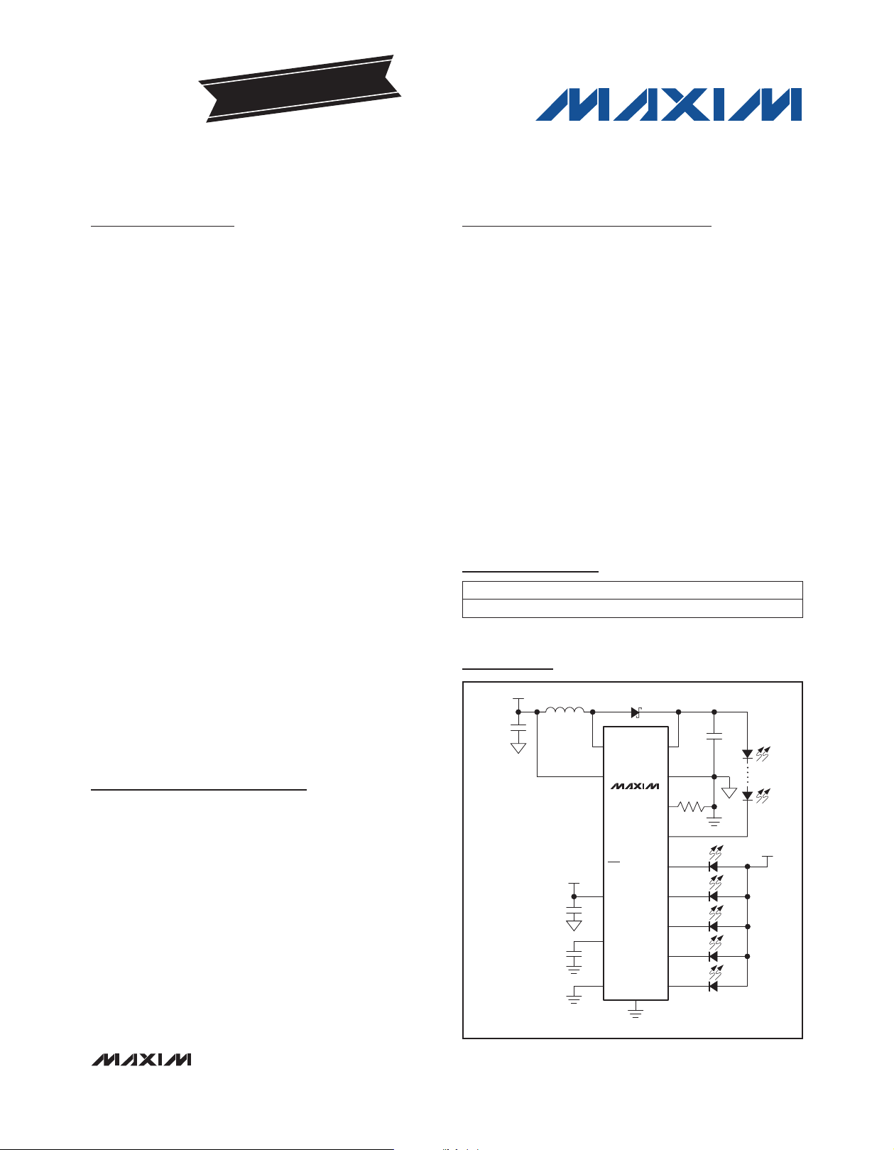
Typical Operating Circuit
2.7V TO 5.0V
2.2FF
0.1FF
47nF
10µH
1.7V TO V+
LX
V+
MAX6948B
SCL
SCL
SDA
SDA
RST
RST
V
DD
COMP
AD0
GND
OUT
PGND
LEDSW
0.22FF
R
B
FB
V
EXT
P0
P1
P2
P3
P4
B
G
R
MAX6948B
NOTE: RB = 0.2V/I
_______________________________________________________________ Maxim Integrated Products 1
= 0.2V/0.03A = 6.7I.
LED
For pricing, delivery, and ordering information, please contact Maxim Direct at 1-888-629-4642,
or visit Maxim’s website at www.maxim-ic.com.
Page 2

High-Efficiency PWM LED Driver with Boost
Converter and Five Constant-Current GPIO Ports
ABSOLUTE MAXIMUM RATINGS
V+ to GND ...............................................................-0.3V to +6V
VDD, COMP to GND ....................................-0.3V to (V+ + 0.3V)
PGND to GND ......................................................-0.3V to +0.3V
LX to PGND (Note 1) .............................................-0.3V to +30V
Current into LX (Note 1) ...................................................700mA
OUT, LEDSW to PGND (Note 1) ...........................-0.3V to +30V
P0–P4 to GND .........................................................-0.3V to +6V
RST, SDA, SCL, AD0 to GND .................. -0.3V to (VDD + 0.3V)
FB to PGND (Note 1) ............................................-0.3V to +0.3V
MAX6948B
I.C. to GND ........................................................... -0.3V to +0.3V
DC Current on P0–P4 .........................................................50mA
DC Current on SDA ............................................................10mA
Total GND Current ............................................................150mA
Total PGND Current .........................................................150mA
Note 1: LX, FB, LEDSW pins have an internal clamp diode to PGND. Applications that forward bias these diodes should take care
not to exceed the power dissipation limits of the device.
Note 2: Package thermal resistances were obtained using the method described in JEDEC specification JESD51-7, using a
single-layer board. For detailed information on package thermal considerations, refer to www.maxim-ic.com/thermal-
tutorial.
Note 3: Refer to the Pb-free solder reflow requirement in J-STD -020, Rev D.1.
Stresses beyond those listed under “Absolute Maximum Ratings” may cause permanent damage to the device. These are stress ratings only, and functional operation of the device at these or any other conditions beyond those indicated in the operational sections of the specifications is not implied. Exposure to absolute
maximum rating conditions for extended periods may affect device reliability.
Continuous Power Dissipation (TA = +70NC)
25-Bump WLP (derate 10.8mW/NC above +70NC) ......866mW
Junction-to-Ambient Thermal Resistance (BJA) (Note 2)
25-Bump WLP ..............................................................93NC/W
Operating Temperature Range
(T
to T
MIN
Junction Temperature .....................................................+150NC
Storage Temperature Range ............................ -65NC to +150NC
ESD Protection
Human Body Model (RD = 1.5kI, CS = 100pF)
P0–P4, OUT, LEDSW, FB to GND ................................Q8kV
All Other Pins ................................................................Q2kV
Lead Temperature (soldering, 10s)
25-Bump WLP ............................................................. (Note 3)
) .............................................. -40NC to +105NC
MAX
ELECTRICAL CHARACTERISTICS
(Typical Application Circuit, V+ = 2.7V to 5.0V, VDD = 1.7V to V+, TA = T
V+ = 3.3V, V
Operating Supply Voltage (V+) V+ 2.7 3.3 5.0 V
Operating Supply Voltage (VDD) V
Output Load External Supply
Voltage
Port External Supply Voltage V
Port Voltage (P0, P4) V
Power-On-Reset Voltage V
Standby Current I
Standby Current in Reset
(Interface Active)
= 2.5V, TA = +25NC.) (Note 4)
DD
PARAMETER SYMBOL CONDITIONS MIN TYP MAX UNITS
DD
V
OUT
EXT
PORT
POR
STBY
I
RST
Boost-converter output 28 V
P0–P4 at high impedance 5.5 V
Constant-current on V+ V
Voltage rising 1.7 V
Standby mode,
boost converter off,
RST = VDD, all digi-
tal inputs at VDD or
GND
Standby mode,
RST = GND,
f
= 400kHz, all
SCL
other digital inputs
at VDD or GND
to T
MIN
TA = +25NC 1.5 4
TA = T
TA = +25NC 1.6 4
TA = T
, unless otherwise noted. Typical values are at
MAX
1.7 2.5 V+ V
to T
MIN
MIN
to T
MAX
MAX
6
6
FA
FA
2
Page 3
High-Efficiency PWM LED Driver with Boost
Converter and Five Constant-Current GPIO Ports
ELECTRICAL CHARACTERISTICS (continued)
(Typical Application Circuit, V+ = 2.7V to 5.0V, VDD = 1.7V to V+, TA = T
V+ = 3.3V, V
= 2.5V, TA = +25NC.) (Note 4)
DD
PARAMETER SYMBOL CONDITIONS MIN TYP MAX UNITS
MIN
to T
, unless otherwise noted. Typical values are at
MAX
MAX6948B
One port set to
Change in Supply Current per
30mA Port
Change in Supply Current per
10mA Port
GPIO PORTS (P0–P4)
Input High Voltage V
Input Low Voltage V
Input Leakage Current I
Input Capacitance 10 pF
30mA Port Sink Constant Current
(P0, P1)
10mA Port Sink Constant Current
(P2, P3, P4)
Logic Output Low Voltage V
DI
DD30
DI
DD10
IH1
IL1
IN
I
PORT30
I
PORT10
OL1
30mA constant current; all other ports
are digital inputs at
VDD or GND
One port set to 5mA
constant current
half-current setting;
all other ports are
digital inputs at VDD
or GND
Port I/O register value set to 0x01
Port I/O register value set to 0x01
Port I/O register
value set to 0x02,
V+ = 3.3V, V
V
LED
(Note 5)
5mA half-current
setting, port I/O
register value set
to 0x02, V+ = 3.3V,
V
- V
EXT
to 1.5V (Note 5)
I
SINK
0x00
EXT
= 0.5V to 1.5V
= 0.5V
LED
= 2mA, port I/O register value set to
TA = +25NC 3 6.2
TA = T
TA = +25NC 1.3 1.7
TA = T
TA = +25NC 27 30 34
-
TA = T
TA = +25NC 4.4 5 5.6
TA = T
MIN
MIN
MIN
MIN
to T
to T
to T
to T
MAX
MAX
MAX
MAX
(0.7 x
VDD)
25 35
3.7 6.3
mA
7
mA
2
(0.3 x
VDD)
±0.03 Q1 FA
mA
mA
0.17 0.3 V
V
V
30mA Port Sink Constant-Current
Matching (P0, P1)
10mA Port Sink Constant-Current
Matching (P2, P3, P4)
Constant-Current Slew Time
DI
PORT30
DI
PORT10
Constant current set
to 30mA, V+ = 3.3V,
TA = +25NC (Note 6)
Constant current set
to 5mA half-current
setting, V+ = 3.3V,
TA = +25NC (Note 6)
20% current to 80% current, port I/O register value changed from 0x01 to 0x02
V
= 1V Q0.7 Q5
PORT
V
= 2.75V Q5
PORT
V
= 1V Q2 Q5 %
PORT
%
2 Fs
3
Page 4
High-Efficiency PWM LED Driver with Boost
Converter and Five Constant-Current GPIO Ports
ELECTRICAL CHARACTERISTICS (continued)
(Typical Application Circuit, V+ = 2.7V to 5.0V, VDD = 1.7V to V+, TA = T
V+ = 3.3V, V
BOOST CONVERTER
Undervoltage Lockout Threshold V
Undervoltage Lockout Threshold
Hysteresis
MAX6948B
Continuous Output Current I
Operating Current
LX Current Limit V+ = 3.3V, TA = +25°C 430 500 570 mA
LX Saturation Voltage ILX = 200mA 0.1 0.25 V
LX Leakage Current I
OUT Leakage Current I
Operating Frequency f
Minimum Duty Cycle
Maximum Duty Cycle 95 %
GM Amplifier Transconductance 250 FS
FB Leakage Current I
Feedback Output Voltage V
Quick-Start Charge Current I
Quick-Start Time
Shutdown Discharge Resistance R
Output Current Line Regulation 3.0V < V+ < 5.0V 2 %/V
Thermal Shutdown Threshold 150 NC
Thermal Shutdown Threshold
Hysteresis
Overvoltage Threshold V
Overvoltage Threshold
Hysteresis
SERIAL INTERFACE (SDA, SCL, AD0, RST)
Input High Voltage V
Input Low Voltage V
Input Leakage Current I
Output Low Voltage SDA V
Input Capacitance C
= 2.5V, TA = +25NC.) (Note 4)
DD
PARAMETER SYMBOL CONDITIONS MIN TYP MAX UNITS
UVLO
V
HYS
WLED
LXOFF
OUTOFFVOUT
BOOST
FB
FB
QS
COMP
OV
V
OV_HYS
IH2
IL2
IN2
OL2
IN2
V+ rising 2.65
V+ falling 2.3
100% boost LED PWM, full-current setting,
RB = 6.67I, I
Run bit = 1, boost standby bit = 0, 0%
boost LED PWM
0% boost LED PWM, VLX = 10V 8 FA
= 28V, boost converter in shutdown 16 23 FA
Continuous conduction mode 10
Discontinuous conduction mode 0
VFB = 100mV ±0.01 Q1 FA
Half-current setting, V+ = 3.3V, TA = +25°C 94 100 106
Full-current setting, V+ = 3.3V, TA = +25°C 190 200 210
Half-current setting 90 100 110
Full-current setting 175 200 225
From enable command STOP condition to
output regulation, C
(Note 7)
V
Rising 28 29 30 V
OUT
I
= 6mA 0.3 V
SINK
WLED
= VFB/R
COMP
to T
MIN
B
= 0.047FF
, unless otherwise noted. Typical values are at
MAX
30 mV
30 mA
2 mA
2 MHz
150 FA
3.5 5 ms
20 kI
9 NC
4 V
0.7 x
V
DD
0.3 x
V
DD
0.03 FA
10 pF
V
%
mV
V
V
4
Page 5
High-Efficiency PWM LED Driver with Boost
Converter and Five Constant-Current GPIO Ports
TIMING CHARACTERISTICS
(Typical Application Circuit, V+ = 2.7V to 5.0V, VDD = 1.7V to V+, TA = T
V+ = 3.3V, VDD = 2.5V, TA = +25NC.) (Note 4)
PARAMETER SYMBOL CONDITIONS MIN TYP MAX UNITS
Internal Boost-Converter PWM
Clock Frequency
Internal GPIO PWM Clock
Frequency
SCL Serial-Clock Frequency f
Bus Free Time Between a STOP
and START Condition
Hold Time (Repeated) START
Condition
Repeated START Condition Setup
Time
STOP Condition Setup Time t
Data Hold Time t
Data Setup Time t
SCL Clock Low Period t
SCL Clock High Period t
Rise Time of Both SDA and SCL
Signals, Receiving
Fall Time of Both SDA and SCL
Signals, Receiving
Fall Time of SDA Transmitting t
Pulse Width of Spike Suppressed t
Serial Bus Timeout t
Capacitive Load for Each Bus
Line
RST Pulse Width
f
INT_
BOOST
f
INT_GPIO
SCL
t
BUF
t
HD, STA
t
SU, STA
SU, STO
HD, DAT
SU, DAT
LOW
HIGH
t
R
t
F
F, TX
SP
OUT
C
b
t
W
(Note 8) 0.9
(Notes 7, 9)
(Notes 7, 9)
(Notes 7, 9)
(Notes 7, 10) 50 ns
(Note 7) 400 pF
MIN
to T
, unless otherwise noted. Typical values are at
MAX
98 125 145 kHz
24 31.25 38 kHz
400 kHz
1.3
0.6
0.6
0.6
180 ns
1.3
0.7
20 +
0.1C
20 +
0.1C
20 +
0.1C
20 30 50 ms
1
b
b
b
300 ns
300 ns
250 ns
Fs
Fs
Fs
Fs
Fs
Fs
Fs
Fs
MAX6948B
Note 4: All parameters are tested at TA = +25NC. Specifications over temperature are guaranteed by design.
Note 5: The DI
Note 6: Current matching is defined as the percent error of any individual port from the average current of the maximum value
measured and the minimum value measured. It can be found using the equation DI
I
Note 7: Guaranteed by design.
Note 8: A master device must provide a hold time of at least 300ns for the SDA signal (referred to VIL of the SCL signal) to
Note 9: I
Note 10: Input filters on the SDA, SCL, and AD0 inputs suppress noise spikes less than 50ns.
MMAVG
bridge the undefined region of SCL’s falling edge.
SINK
specifies current matching between ports of a single part.
PORT_
= 100 x (I
where I
P 6mA. Cb = total capacitance of one bus line in pF. tR and tF are measured between 0.3 x V
MMAVG
= (I
MEASMAX
+ I
MEASMIN
)/2.
PORT_
- I
MMAVG
and 0.7 x VDD.
DD
MEAS
)/
5
Page 6
High-Efficiency PWM LED Driver with Boost
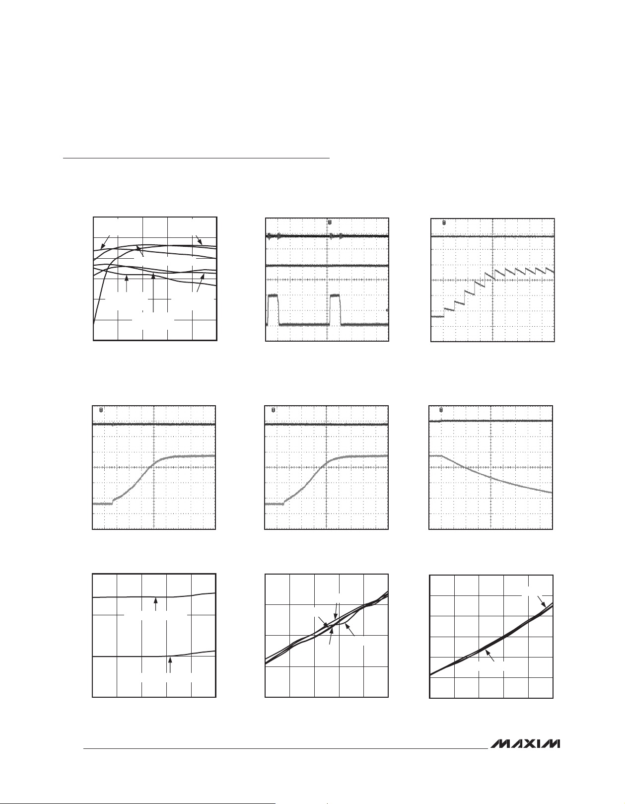
MAX6948B toc08
5.00
Converter and Five Constant-Current GPIO Ports
Typical Operating Characteristics
(V+ = 3.3V, VDD = 2.5V, TA = +25NC, unless otherwise noted.)
90
FULL-CURRENT
3 LEDs
85
MAX6948B
80
75
EFFICIENCY (%)
70
65
60
2.70 5.25
FULL-CURRENT 5 LEDs
HALF-CURRENT
3 LEDs
HALF-CURRENT
5 LEDs
V+ (V)
SOFT-START V+, V
500mV/div
V+
5V/div
V
OUT
EFFICIENCY vs. V+
FULL-CURRENT
HALF-CURRENT
(512/1024)
OUT
7 LEDs
7 LEDs
4.744.233.723.21
MAX6948B toc04
500mV/div
MAX6948B toc01
500mV/div
5V/div
V
OUT
10V/div
GND
5V/div
V
OUT
V+
LX
V+
SWITCHING WAVEFORMS
SOFT-START V+, V
(1024/1024)
OUT
MAX6948B toc02
MAX6948B toc05
500mV/div
5V/div
V
OUT
SOFT-START V+, V
V+
SHUTDOWN RESPONSE (V+, V
(10/1024)
OUT
MAX6948B toc03
OUT)
MAX6948B toc06
500mV/div
V+
5V/div
V
OUT
GND
(mA)
WLED
I
I
30mA OUTPUT CURRENT vs. V+
WLED
35
MAX6948B toc07
25
15
5
FULL-CURRENT 6 LEDs
HALF-CURRENT 6 LEDs
V+ (V)
V+ (V)
STANDBY CURRENT (µA)
4.544.083.623.162.70 5.00
STANDBY CURRENT I
4
3
2
1
0
+25NC
-40NC
V+ (V)
+105NC
RST
vs. V+
+85NC
4.544.083.623.162.70
STANDBY CURRENT I
5.8
5.7
5.6
5.5
5.4
STANDBY CURRENT (mA)
5.3
5.2
STBY
+25NC, +85NC, +105NC
V+ (V)
vs. V+
-40NC
MAX6948B toc09
4.544.083.623.162.70 5.00
6
Page 7
High-Efficiency PWM LED Driver with Boost
V+ (V)
Converter and Five Constant-Current GPIO Ports
Typical Operating Characteristics (continued)
(V+ = 3.3V, VDD = 2.5V, TA = +25NC, unless otherwise noted.)
MAX6948B
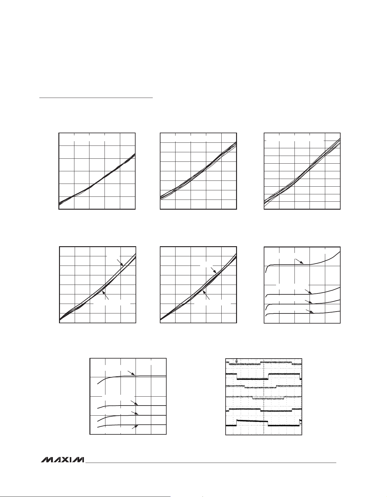
SUPPLY CURRENT vs. V+
(BOOST ON, 10% PWM,
FULL CURRENT AND HALF CURRENT)
6.0
TA = -40NC, +25NC, +85NC, +105NC
5.9
5.8
5.7
5.6
SUPPLY CURRENT (mA)
5.5
5.4
DELTA SUPPLY CURRENT P0 vs. V+
(DIFFERENCE IN CURRENT FROM
PORT OFF TO ON)
5.70
5.65
5.60
5.55
5.50
5.45
5.40
DELTA SUPPLY CURRENT P0 (mA)
5.35
5.30
+25NC, +85NC, +105NC
4.544.083.623.162.70 5.00
-40NC
4.544.083.623.162.70 5.00
SUPPLY CURRENT vs. V+
(BOOST ON, 50% PWM,
FULL CURRENT AND HALF CURRENT)
6.5
TA = -40NC, +25NC, +85NC, +105NC
6.4
MAX6948B toc10
6.3
6.2
6.1
6.0
SUPPLY CURRENT (mA)
5.9
5.8
5.7
DELTA SUPPLY CURRENT P2 vs. V+
(DIFFERENCE IN CURRENT
FROM PORT OFF TO ON)
5.70
5.65
MAX6948B toc13
5.60
5.55
5.50
5.45
5.40
DELTA SUPPLY CURRENT P2 (mA)
5.35
5.30
4.544.083.623.162.70 5.00
-40NC
+25NC, +85NC, +105NC
4.544.083.623.162.70 5.00
V+ (V)
FULL CURRENT AND HALF CURRENT)
7.2
TA = -40NC, +25NC, +85NC, +105NC
7.1
7.0
MAX6948B toc11
6.9
6.8
6.7
6.6
6.5
SUPPLY CURRENT (mA)
6.4
6.3
6.2
40
MAX6948B toc14
OUTPUT SINKING CURRENT (mA)
FULL-CURRENT PO
30
20
FULL-CURRENT P2
10
0
0 5
SUPPLY CURRENT vs. V+
(BOOST ON, 10% PWM,
4.544.083.623.162.70 5.00
OUTPUT SINKING CURRENT
vs. V
PORT
V+ = 5V
HALF-CURRENT PO
HALF-CURRENT P2
V
(V)
PORT
MAX6948B toc12
MAX6948B toc15
4321
OUTPUT SINKING CURRENT
vs. V
V
PORT
PORT
(V)
40
FULL-CURRENT PO
30
20
10
OUTPUT SINKING CURRENT (mA)
0
HALF-CURRENT PO
FULL-CURRENT P2
HALF-CURRENT P2
0 1.0
V+ = 5V
0.80.60.40.2
MAX6948B toc16
BOOST
STAGGER PWM PORT WAVEFORMS
vs. TIME ALL (50% PWM)
P0
P2
P3
P1
P4
1ms/div
MAX6948B toc17
7
Page 8
High-Efficiency PWM LED Driver with Boost
Converter and Five Constant-Current GPIO Ports
Pin Configuration
TOP VIEW
(BUMP IN BOTTOM)
MAX6948B
SCL SDA V+
AD0 V+ V+
WLP
MAX6948B
P0
A1
P1
B1 B2 B3 B4 B5
P2
C1 C2 C3 C4 C5
P3
D1 D2 D3 D4 D5
P4
E1 E2 E3 E4 E5
RST
A2 A3 A4 A5
V
DD
GND N.C. I.C. COMP
GND FB PGND PGND
OUT LEDSW LX LX
(2.31mm x 2.31mm)
Pin Description
PIN NAME FUNCTION
A1 P0 GPIO Port. Open-drain I/O. P0 can be configured as a 30mA (max) constant sink current output.
A2
RST
A3 SCL I2C-Compatible, Serial-Clock Input
A4 SDA I2C-Compatible, Serial-Data I/O
A5, B4, B5 V+
B1 P1 GPIO Port. Open-drain I/O. P1 can be configured as a 30mA (max) constant sink current output.
B2 V
DD
B3 AD0 Address Input. AD0 selects up to four device slave addresses (Table 13).
C1 P2 GPIO Port. Open-drain I/O. P2 can be configured as a 10mA (max) constant sink current output.
C2, D2 GND Ground. Connect to PGND.
C3 N.C. No Connection. Internally not connected.
C4 I.C. Internally Connected. Connect I.C. to GND for normal operation.
C5 COMP
D1 P3 GPIO Port. Open-drain I/O. P3 can be configured as a 10mA maximum constant sink current output.
D3 FB
D4, D5 PGND Power Ground. Connect PGND to GND.
E1 P4 GPIO Port. Open-drain I/O. P4 can be configured as a 10mA (max) constant sink current output.
E2 OUT Output Voltage Sense Input for Boost Converter
E3 LEDSW High-Voltage, Constant-Current Input. Connect LEDSW to the cathode-end of the WLED string.
E4, E5 LX Inductor Switch Node
Active-Low Reset Input
Boost-Converter Supply Voltage and Positive Supply Voltage. Bypass V+ to GND with a 2.2FF or
higher value ceramic capacitor.
I2C Logic Supply Voltage. Bypass VDD to GND with a 0.1FF or higher value ceramic capacitor.
Compensation Terminal for the Boost Converter. A capacitor from COMP to PGND determines the
boost-converter stability.
Load Current-Sense Voltage Feedback for the Boost Converter. A resistor between FB and PGND
sets the maximum load current.
8
Page 9
High-Efficiency PWM LED Driver with Boost
Converter and Five Constant-Current GPIO Ports
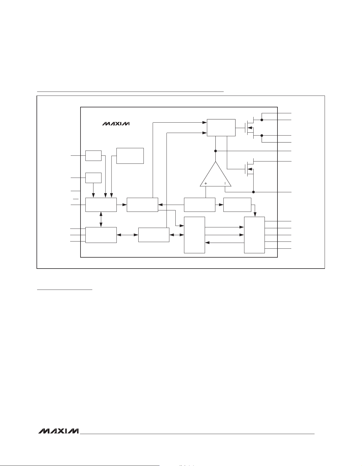
Functional Block Diagram
LX
LX
OUT
V
PWM AND
MAX6948B
V+
UVLO
OVP
DD
THERMAL
SHUTDOWN
GATE DRIVE
n-CHANNEL
MOSFET
n-CHANNEL
MOSFET
PGND
PGND
COMP
LEDSW
FB
MAX6948B
RST
SDA
SCL
ADO
POR
I2C
INTERFACE
125kHz, 31.25kHz
OSCILLATOR
CONTROL
REGISTERS
Detailed Description
The MAX6948B general-purpose input/output (GPIO)
peripheral with integrated boost converter provides a
boost converter capable of driving 6 WLEDs and five I/O
ports capable of driving LEDs powered from an alternate
power supply such as the Li+ battery. The integrated
2MHz boost converter minimizes the size and cost of
external components and supplies 30mA of load current
at up to 28V. The feedback input to the error amplifier
has a typical set point of 0.1V to minimize power dissipation. External compensation keeps the converter
stable under all load conditions from 5V up to 28V. The
MAX6948B includes overvoltage and open-circuit detection to prevent damage to the IC.
An I2C-programmable 10-bit PWM signal enables 1024
levels of WLED intensity. During PWM off-time, the
internal switch at the LEDSW pin disconnects the series
WLEDs. This limits the PWM off-time leakage current to
a minimum, limited only by the PWM switch internal to
the MAX6948B. Consequently, the boost output voltage
BANDGAP
REFERENCE
PWM AND
GPIO LOGIC
LED ENABLE
GPIO ENABLE
GPIO INPUT
CURRENT
DAC
PORT GPIO
AND
CONSTANT-
CURRENT
LED DRIVE
P0
P1
P2
P3
P4
remains almost constant during PWM on-/off-time periods. This new approach provides advantages of minimal
WLED color change for sharp WLED on and off, and
more power efficiency due to minimal leakage.
The five GPIO ports function as logic inputs, opendrain logic outputs, or constant-current sinks in any
combination. Ports withstand 5.5V independent of the
MAX6948B’s supply voltage. Two of the ports drive
additional LEDs up to 30mA, while the other three ports
drive LEDs at up to 10mA/port. The MAX6948B features
shutdown and standby modes for low-power dissipation. The constant-current drivers contain programmable
PWM outputs and allow staggering to reduce the input
peak current requirements. The I/O ports also feature
ramp-up and ramp-down controls.
The MAX6948B features a single input to select from four
I2C slave addresses. Programming and functionality for
the five GPIO ports is identical to the MAX6946/MAX6947
I/O expanders.
9
Page 10

High-Efficiency PWM LED Driver with Boost
Converter and Five Constant-Current GPIO Ports
Register Description
The MAX6948B contains 25 internal registers (Table 1).
Registers 0x00 to 0x15 control ports P0–P4 and remain
Register 0x20 and 0x21 set the PWM duty cycle for the
integrated boost converter. Register 0x22 conveys the
boost-converter status.
compatible with the MAX6946/MAX6947 port expanders.
Table 1. Register Address Map and Autoincrement Address
ADDRESS
CODE (hex)
MAX6948B
0x00 0x01 R/W P0 Port P0 I/O control and PWM settings
0x01 0x02 R/W P1 Port P1 I/O control and PWM settings
0x02 0x03 R/W P2 Port P2 I/O control and PWM settings
0x03 0x04 R/W P3 Port P3 I/O control and PWM settings
0x04 0x10 R/W P4 Port P4 I/O control and PWM settings
0x05 — — Reserved —
0x06 — — Reserved —
0x07 — — Reserved —
0x08 — — Reserved —
0x09 — — Reserved —
0x0A 0x10 R/W
0x0B 0x10 R/W
0x0C 0x10 R/W
0x0D 0x10 — Reserved —
0x0E 0x0E Read only Port input Reads GPIO input values
0x0F — — Reserved —
0x10 0x11 R/W Configuration
0x11 0x12 R/W Ramp-down Port ramp-down and hold-off settings
0x12 0x13 R/W Ramp-up Port ramp-up setting
0x13 0x14 R/W Output current Port half-/full-current settings
0x14 — — Reserved —
0x15 0x10 R/W Global current Port maximum current setting
0x20 0x21 R/W
0x21 — R/W Boost PWM (LSB) Boost circuit LED PWM setting (LSB)
0x22 — R/W Boost status Boost circuit status and standby setting
AUTO-INCREMENT
ADDRESS (hex)
READ/
WRITE
REGISTER
FUNCTION
Group control
(P0–P4)
Group control
(P0, P1)
Group control
(P2, P3, P4)
Boost PWM
(MSB)
Write: Simultaneously sets I/O and PWM settings for
ports P0–P4
Read: Reads contents of address 0x00
Write: Simultaneously sets I/O and PWM settings for
ports P0, P1
Read: Reads contents of address 0x00
Write: Simultaneously sets I/O and PWM settings for
ports P2, P3, P4
Read: Reads contents of address 0x00
Half-/full-boost current, reset options, PWM stagger,
start/stop status, reset run, shutdown setting
Boost circuit LED PWM setting (MSB)
DESCRIPTION
10
Page 11
High-Efficiency PWM LED Driver with Boost
Converter and Five Constant-Current GPIO Ports
Configuration Register Format (0x10)
Use the configuration register to select PWM phasing
between outputs, monitor fade status, enable hardware
startup from shutdown, and select shutdown or run mode
(Table 2).
Table 2. Configuration Register Format (0x10)
REGISTER BIT DESCRIPTION VALUE FUNCTION DEFAULT VALUE
D7 Half-/full-boost current
D6 Reset/POR option
D5 PWM stagger
D4 Hold-off status
D3 Ramp-down (fade-off) status
D2 Ramp-up status
D1 Reset-run enable
D0 Run
1 Half-boost current set by R
0 Full-boost current set by R
0
1
0 PWM outputs are in phase
1 PWM outputs are staggered
0 Device is not in hold-off
1 Device is in hold-off
0 Device is not in fade-off
1 Device is in fade-off
0 Device is not in ramp-up
1 Device is in ramp-up
0 Reset run disabled
1 Reset run enabled
0 Shutdown mode
1 Run mode
Initial Power-Up
On power-up, all control registers are set to powerup values and the MAX6948B is in shutdown mode
(Table 3).
FB
FB
RST does not change register data
RST resets registers to POR values
1
0
0
Read only
Read only
Read only
0
0
MAX6948B
Table 3. Power-On Reset (POR) Values
ADDRESS
CODE (hex)
0x00 R/W 0xFF P0 Port P0 high impedance
0x01 R/W 0xFF P1 Port P1 high impedance
0x02 R/W 0xFF P2 Port P2 high impedance
0x03 R/W 0xFF P3 Port P3 high impedance
0x04 R/W 0xFF P4 Port P4 high impedance
0x10 R/W 0x00 Configuration Shutdown mode (reset run disabled)
0x11 R/W 0x00 Ramp-down Port ramp-down and hold-off disabled
0x12 R/W 0x00 Ramp-up Port ramp-up disabled
0x13 R/W 0x03 Output current P0, P1 at full current; P2, P3, P4 at half current
0x15 R/W 0x07 Global current Maximum output current
0x20 R/W 0x00 Boost PWM (MSB) Zero PWM duty cycle
0x21 R/W 0x00 Boost PWM (LSB) Zero PWM duty cycle
0x22 R/W 0x01 Boost status Boost circuit in standby mode
READ/
WRITE
POWER-UP
VALUE (hex)
REGISTER FUNCTION POR DESCRIPTION
11
Page 12

High-Efficiency PWM LED Driver with Boost
Converter and Five Constant-Current GPIO Ports
Boost Converter
in a single register (0x20) to allow a single I2C write to
set the majority of the intensity level and minimize visible
Boost-Converter Output PWM
The MAX6948B boost converter has 10-bit PWM opera-
flicker during intensity changes. The LSB register (0x21)
allows for very fine adjustments in LED intensity.
tion using an internal 125kHz clock. This yields a PWM
period of 1024/125k = 8.192ms. PWM operation allows
the user to adjust the LED intensity and lower the average
current by enabling and disabling the boost converter at
a selectable rate. This rate is set using the boost-converter output PWM registers (Tables 4, 5). The duty cycle
MAX6948B
ranges from 0/1024 (no intensity or off) to 1023/1024 (full
intensity). Eight of the 10 bits, which include the MSB, are
The MAX6948B checks the boost converter and indicates its status in the boost-converter status register
(Table 6). Faults indicated in this register include thermal shutdown, overvoltage, and current limit. The boost
converter goes into standby mode whenever the boost
standby bit (D0) = 1.
Boost-Converter Status Register
Table 4. Boost-Converter Output PWM (MSB) Register Format (0x20)
REGISTER BIT DESCRIPTION VALUE FUNCTION DEFAULT VALUE
D7 Bit 9 — Boost-converter output PWM bit 9 (MSB) 0
D6 Bit 8 — Boost-converter output PWM bit 8 0
D5 Bit 7 — Boost-converter output PWM bit 7 0
D4 Bit 6 — Boost-converter output PWM bit 6 0
D3 Bit 5 — Boost-converter output PWM bit 5 0
D2 Bit 4 — Boost-converter output PWM bit 4 0
D1 Bit 3 — Boost-converter output PWM bit 3 0
D0 Bit 2 — Boost-converter output PWM bit 2 0
X = Don’t care.
Table 5. Boost-Converter Output PWM (LSB) Register Format (0x21)
REGISTER BIT DESCRIPTION VALUE FUNCTION DEFAULT VALUE
D7–D2 Reserved 000000 — 000000
D1 Bit 1 — Boost-converter output PWM bit 1 0
D0 Bit 0 — Boost-converter output PWM bit 0 (LSB) 0
Table 6. Boost-Converter Status Register Format (0x22)
REGISTER BIT DESCRIPTION VALUE FUNCTION DEFAULT VALUE
D7, D6, D5 Reserved 000 — 000
D4 Schottky open
D3 Current limit
D2 Thermal shutdown
D1 Overvoltage
D0 Boost standby
0 Schottky diode present
1 Schottky diode open
0 Normal output current
1 Converter output current exceeded the current limit
0 Normal operation
1
0 Normal operation
1 V
0
1 Boost converter in standby mode
Device temperature has exceeded thermal
shutdown threshold
exceeded overvoltage limit
OUT
Boost converter operating according to PWM
register and configuration register
Read only
Read only
Read only
Read only
1
12
Page 13

High-Efficiency PWM LED Driver with Boost
Converter and Five Constant-Current GPIO Ports
Boost-Converter Shutdown/Standby Modes
The boost converter shuts down when D0 of the configuration register (0x10) = 0, or when D0 of the boostconverter status register (0x22) = 1. If both the boost
PWM output registers’ (0x20, 0x21) values are zero, the
boost converter remains in a low-current state (standby).
Undervoltage Lockout (UVLO)
Undervoltage lockout (UVLO) disables the boost converter when V+ is below 2.4V (max). This resets bit D0
of the configuration register and puts the part into shutdown mode (0x10).
Quick Start
The MAX6948B quick starts by charging C
current source. During this time, the internal MOSFET
is switching at the minimum duty cycle. Once V
rises above 0.2V, the duty cycle increases until the
output voltage reaches the desired regulation level. In
shutdown mode, COMP is pulled to GND with a 20kI
internal resistor.
Overvoltage Protection
If the voltage on the output terminal rises above 28.5V
(min), the converter is put into standby mode. This protects the converter from excessive voltage in the event
of an open-circuit condition. To detect if the boost converter has exceeded the overvoltage limit, read bit D1
of the boost-converter status register (0x22). Once the
output voltage has dropped 4V below the overvoltage
threshold, the read-only bit (D1) goes to zero. The boost
converter leaves standby mode and normal operation
resumes. Reading the register causes the bit to reset. If
the fault is still active, the bit will be set again.
COMP
with a
COMP
Thermal shutdown limits total power dissipation in the
MAX6948B. When the junction temperature exceeds
151NC (typ), the boost converter and ports P0–P4 turn
off, allowing the part to cool. The thermal shutdown bit
(D2) of the boost configuration and status register (0x22)
is set high. Bit D0 of the boost-converter status register
(0x22) = 1, bit D0 of the configuration register (0x10)
= 0 (reset), and the device is in shutdown mode. The
MAX6948B turns on and begins to quick-start after the
junction temperature cools by 10NC. Reading this register causes the bit to reset. If the fault is still active, the bit
will be set again.
The MAX6948B current-limit function monitors the inductor current when the internal switch on the LX node is
on. The device compares the inductor current to a fixed
threshold. When the current exceeds the threshold, bit
D3 of the boost-converter status register asserts and
the switch shuts off for that cycle. Reading this register
causes the bit to reset. If the fault is still active, the bit
will be set again.
Boost-Converter Current Settings
The boost current, through the serial output LEDs, can
be set to half or full scale by setting the FB pin voltage.
The FB voltage is set through bit D7 of the configuration
register (0x10) (Table 2). The FB voltage settings are
100mV or 200mV for half- or full-current mode operation,
respectively.
Thermal Shutdown
Current Limit
MAX6948B
13
Page 14

High-Efficiency PWM LED Driver with Boost
Converter and Five Constant-Current GPIO Ports
I/O Ports (P0–P4)
The MAX6948B contains five I/O ports (P0–P4). Configure
the five I/O ports as logic inputs, open-drain logic outputs,
or constant-current sinks in any combination. Table 7
provides a detailed description of the individual port configuration registers. Use registers 0x00 to 0x04 to individually assign each port (see the PWM Intensity Control and
Table 7. Port Registers Format (0x00 to 0x04, 0x0A, 0x0B, and 0x0C)
MAX6948B
REGISTER DESCRIPTION
Port is logic-low. Port is still active in shutdown mode. 0 0 0 0 0 0 0 0
Port is logic-high. Set this mode when using GPIO as an input.
Port is still active when in shutdown mode.
Port is a static constant-current sink. Port is high impedance
when in shutdown mode.
Port is a constant-current sink with a 3/256 duty cycle. Port is
high impedance when in shutdown mode.
Port is a constant-current sink with a 4/256 duty cycle. Port is
high impedance when in shutdown mode.
Port is a constant-current sink with a 5/256 duty cycle. Port is
high impedance when in shutdown mode.
Port is a constant-current sink with a 254/256 duty cycle. Port is
high impedance when in shutdown mode.
Power-up default setting (port is high impedance) 1 1 1 1 1 1 1 1
Phasing section). Use registers 0x0A, 0x0B, and 0x0C to
assign the same port setting to multiple ports (Table 1).
When powered off, the I/O ports remain in high impedance.
Figure 1 shows the I/O port structure of the MAX6948B.
I/O ports P0–P4 default to high impedance on power-up,
to prevent connected ports from drawing current. Ports
used as inputs do not load their source signals.
REGISTER DATA
D7 D6 D5 D4 D3 D2 D1 D0
0 0 0 0 0 0 0 1
0 0 0 0 0 0 1 0
0
0 0 0 0 0 1 0 0
0 0 0 0 0 1 0 1
U
U
U
1 1 1 1 1 1 1 0
0
0 0
0 0
1
1
8-BIT LATCH
OUTPUT PORT
REGISTER
TO/FROM
SERIAL
INTERFACE
Figure 1. Simplified Schematic of I/O Ports
14
1-BIT LATCH
OUTPUT-CURRENT
REGISTER
3-BIT LATCH
GLOBAL-CURRENT
REGISTER
READ I/O
PORT COMMAND
POSITION A: 0x00 TO 0x01
POSITION B: 0x02 TO 0xFF
CLOSE SWITCH: 0x02 TO 0xFE
MSB
4-BIT DAC
PWM
GENERATOR
ENABLE
SET
CURRENT
A B
ENABLE = 0x00
I/O PORT
n-CHANNEL
MOSFET
Page 15
High-Efficiency PWM LED Driver with Boost
Converter and Five Constant-Current GPIO Ports
Ports Configured as Outputs
The global-current register sets the full (maximum)
constant-current sink amount for I/O ports configured as
an output (Table 8). Power-up sets the global current to
its maximum value.
Set each output port’s individual constant-current sink to
either half scale or full scale of the global current. Use
the output-current registers to set the individual currents
Table 8. Global-Current Register Format (0x15)
REGISTER DESCRIPTION
3.75mA full-current value (P0, P1)
1.25mA full-current value (P2, P3, P4)
7.5mA full-current value (P0, P1)
2.5mA full-current value (P2, P3, P4)
11.25mA full-current value (P0, P1)
3.75mA full-current value (P2, P3, P4)
15mA full-current value (P0, P1)
5mA full-current value (P2, P3, P4)
18.75mA full-current value (P0, P1)
6.25mA full-current value (P2, P3, P4)
22.5mA full-current value (P0, P1)
7.5mA full-current value (P2, P3, P4)
26.25mA full-current value (P0, P1)
8.75mA full-current value (P2, P3, P4)
30mA full-current value (P0, P1)
10mA full-current value (P2, P3, P4)
Power-up default 0 0 0 0 0 1 1 1
X = Don’t care.
(Table 9). By default, P0 and P1 start up set to full current, while P2, P3, and P4 are set to half current.
Set each output current individually to best suit the
maximum operating current of an LED load, or adjust as
needed to double the effective intensity control range of
each output. The maximum individual current selection is
15mA (half) or 30mA (full) for ports P0 and P1, and 5mA
(half) or 10mA (full) for ports P2, P3, and P4.
REGISTER DATA
D7 D6 D5 D4 D3 D2 D1 D0
RESERVED GLOBAL CURRENT
X X X X X 0 0 0
X X X X X 0 0 1
X X X X X 0 1 0
X X X X X 0 1 1
X X X X X 1 0 0
X X X X X 1 0 1
X X X X X 1 1 0
X X X X X 1 1 1
MAX6948B
Table 9. Output-Current Register Format (0x13)
REGISTER BIT DESCRIPTION VALUE FUNCTION DEFAULT VALUE
D7, D6, D5 Reserved 0 — 0
D4 P4
D3 P3
D2 P2
D1 P1
D0 P0
0 Port P4 is set to half current
1 Port P4 is set to full current
0 Port P3 is set to half current
1 Port P3 is set to full current
0 Port P2 is set to half current
1 Port P2 is set to full current
0 Port P1 is set to half current
1 Port P1 is set to full current
0 Port P0 is set to half current
1 Port P0 is set to full current
0
0
0
1
1
15
Page 16

High-Efficiency PWM LED Driver with Boost
Converter and Five Constant-Current GPIO Ports
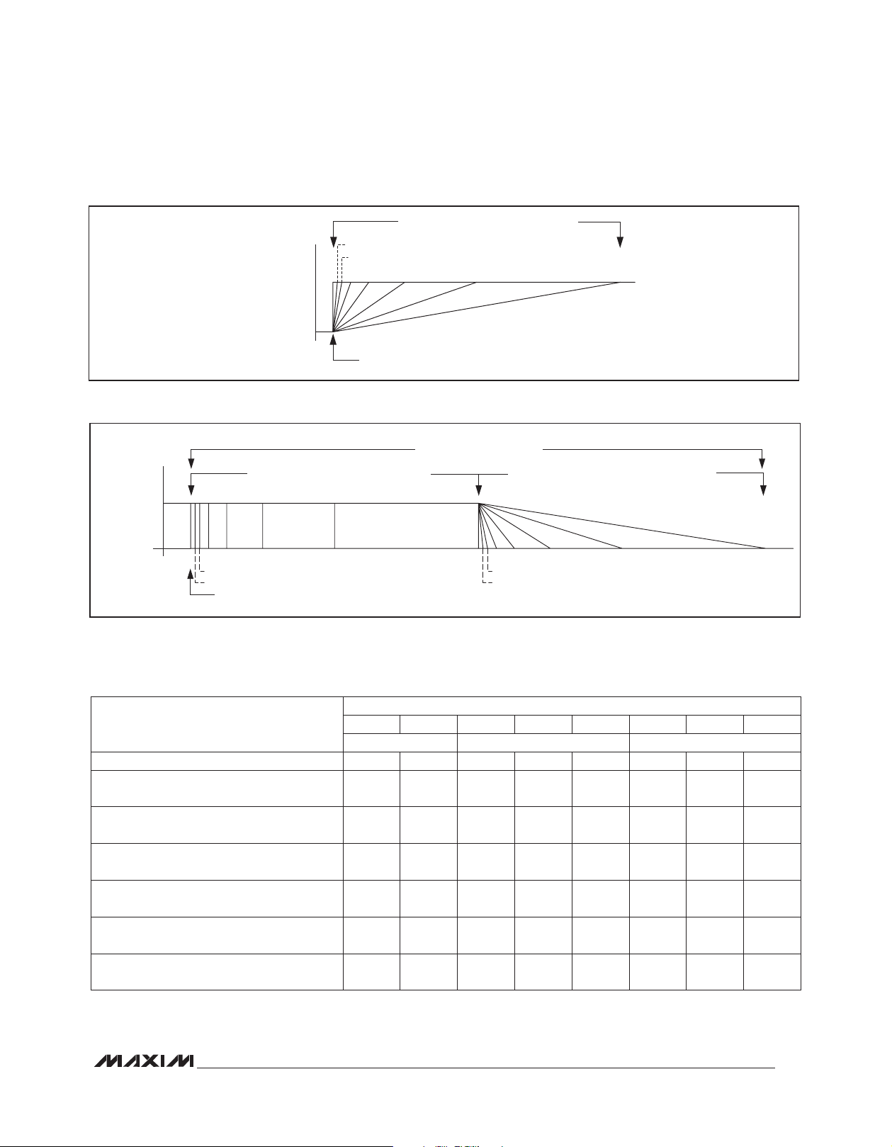
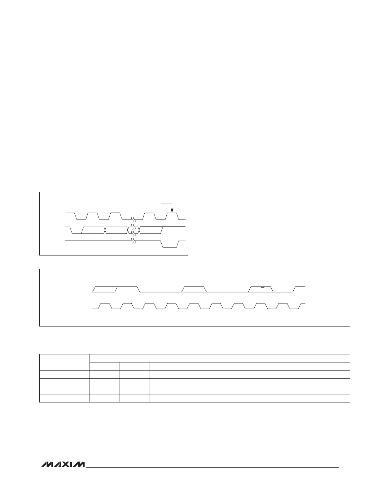
PWM Intensity Control and Phasing
The MAX6948B uses an internal 31.25kHz oscillator to
generate PWM timing for LED intensity control. A PWM
period comprises 256 cycles of the nominal 31.25kHz
PWM clock (Figure 2). Each port can have an individual
PWM duty cycle between 3/256 and 254/256. See Table
7 for port register settings.
Configure PWM timing by setting the stagger bit in the
configuration register (Table 2), either with output stag-
MAX6948B
gering or without. Set PWM stagger = 0 to cause all
outputs using PWM to switch at the same time using the
timing shown in Figure 2. All outputs, therefore, draw
load current at the exact same time for the same PWM
setting. This means that if, for example, all outputs are
OUTPUT
REGISTER
7.8125ms NOMINAL PWM PERIOD
0x00
0x01
0x02
0x03
0x04
VALUE
OUTPUT STATIC-LOW LOGIC DRIVE WITH INPUT BUFFER ENABLED (GPI)
OUTPUT STATIC-HIGH LOGIC DRIVE WITH INPUT BUFFER ENABLED (GPI)
OUTPUT STATIC-LOW CONSTANT CURRENT WITH INPUT BUFFER DISABLED (STATIC LED DRIVE ON)
OUTPUT LOW 3/256 DUTY CONSTANT CURRENT WITH INPUT BUFFER DISABLED (PWM LED DRIVE)
OUTPUT LOW 4/256 DUTY CONSTANT CURRENT WITH INPUT BUFFER DISABLED (PWM LED DRIVE)
set to 0x80 (128/256 duty cycle), the current draw would
be zero (all loads off) for half the time, and full (all loads
on) for the other half.
Set PWM stagger = 1 to stagger the PWM timing of the
five port outputs and the integrated boost-converter output, distributing the port output switching points across
the PWM period (Figure 3). Staggering reduces the di/dt
output-switching transient on the supply and reduces the
peak/mean current requirement.
Change the PWM stagger-setting bit during shutdown.
Changing the stagger bit during normal operation can
cause a transient flicker in any PWM-controlled LED
because of the fundamental PWM timing changes.
HIGH-Z
LOW
HIGH-Z
LOW
HIGH-Z
LOW
HIGH-Z
LOW
HIGH-Z
LOW
0xFC
0xFD
0xFE
0xFF
OUTPUT LOW 252/256 DUTY CONSTANT CURRENT WITH INPUT BUFFER DISABLED (PWM LED DRIVE)
OUTPUT LOW 253/256 DUTY CONSTANT CURRENT WITH INPUT BUFFER DISABLED (PWM LED DRIVE)
OUTPUT LOW 254/256 DUTY CONSTANT CURRENT WITH INPUT BUFFER DISABLED (PWM LED DRIVE)
OUTPUT STATIC HIGH IMPEDANCE WITH INPUT BUFFER DISABLED (STATIC LED DRIVE OFF)
Figure 2. Static and PWM Constant-Current Waveforms
16
HIGH-Z
LOW
HIGH-Z
LOW
HIGH-Z
LOW
HIGH-Z
LOW
Page 17

High-Efficiency PWM LED Driver with Boost
Converter and Five Constant-Current GPIO Ports
MAX6948B
8.192ms NOMINAL PORT PWM PERIOD
42 84 126 168 210 256
PORT 0 OR PORTS AND BOOST IN PHASE
PORT 2 STAGGERED PWM PERIOD
PORT 3 STAGGERED PWM PERIOD
PORT 1 STAGGERED PWM PERIOD
PORT 4 STAGGERED PWM PERIOD
BOOST STAGGERED PWM PERIOD
Figure 3. Staggered Port and Boost PWM Waveform
NEXT PORT PWM PERIOD NEXT PORT PWM PERIOD
PORT 0 OR PORTS AND BOOST IN PHASE
PORT 2 STAGGERED PWM PERIOD
PORT 3 STAGGERED PWM PERIOD
PORT 1 STAGGERED PWM PERIOD
PORT 4 STAGGERED PWM PERIOD
PORT 0 OR PORTS AND BOOST IN PHASE
BOOST STAGGERED PWM PERIOD
Table 10. Input Ports Register Format (0x0E, Read Only)
REGISTER BIT DESCRIPTION VALUE FUNCTION
D7, D6, D5 Reserved 0 —
D4 P4
D3 P3
D2 P2
D1 P1
D0 P0
0 Port P4 is logic input low, or is not set as an input
1 Port P4 is logic input high
0 Port P3 is logic input low, or is not set as an input
1 Port P3 is logic input high
0 Port P2 is logic input low, or is not set as an input
1 Port P2 is logic input high
0 Port P1 is logic input low, or is not set as an input
1 Port P1 is logic input high
0 Port P0 is logic input low, or is not set as an input
1 Port P0 is logic input high
PORT 2 STAGGERED PWM PERIOD
Ports Configured as Inputs
Configure a port as a logic input by writing 0x01 to the
port’s output register (Table 7). Reading an input port
register returns the logic levels from the I/O ports configured as a logic input (Table 10). The input port register
returns logic 0 in the appropriate bit position for a port
not configured as a logic input. The input ports’ registers
are read only. The MAX6948B ignores writes to the input
ports register.
Standby Mode and Operating Current
Configuring all the ports as logic inputs or outputs (all
output registers set to value 0x00 or 0x01) or high impedance (output register set to value 0xFF) puts the device
into standby mode. Put the MAX6948B into standby
mode for lowest supply current consumption.
Setting a port as a constant-current output increases the
operating current (output register set to a value between
0x02 and 0xFE), even if a load is not applied to the
port. The MAX6948B enables an internal current mirror
to provide the accurate constant-current sink. Enabling
the internal current mirror increases the device’s supply
current. Each output contains a gated mirror, which activates only when required.
In PWM mode, the current mirror turns on only for the
duration of the output’s on-time. This means that the
operating current varies as constant-current outputs are
turned on and off through the serial interface, as well as
by the PWM intensity control.
17
Page 18

High-Efficiency PWM LED Driver with Boost
Converter and Five Constant-Current GPIO Ports
Shutdown Mode
In shutdown mode, all ports configured as constantcurrent outputs (output register set to a value between
0x02 and 0xFE) switch off and become high impedance.
Shutdown does not affect ports configured as logic
inputs or outputs (output registers set to value 0x00
or 0x01) (Table 7). This means that any ports used for
GPIOs are still operational in shutdown mode.
Put the MAX6948B into shutdown mode by setting the
MAX6948B
run bit (D0) = 0 in the configuration register (0x10) (Table
2). Exit shutdown by setting the run bit high through the
serial interface or by using the reset-run option (see the
Reset-Run Option section). Configure and control the
MAX6948B normally through the serial interface in shutdown mode. All registers are accessible in shutdown
mode. Entering and/or exiting shutdown mode does not
change any register values.
Changing a port from static logic-low (0x00) or static
logic-high (0x01) to a constant-current value (0x02 to
0xFE) in shutdown mode turns that output off (logic-high
or high impedance) like any other constant-current outputs in shutdown. The new constant-current output starts
just like any other constant-current outputs when exiting
shutdown.
Changing a port from a constant-current value (0x02 to
0xFE) to static logic-low (0x00) or static logic-high (0x01)
in shutdown causes that output to set to the value as a
GPIO output. The new GPIO output is unaffected just like
any other GPIO output when exiting shutdown.
Ramp-Up and Ramp-Down Controls
The MAX6948B provides controls that allow the output
currents to ramp down into shutdown (ramp-down) and
ramp up again out of shutdown (ramp-down) (Figures
4, 5). Ramp-down comprises a programmable hold-off
delay that maintains the outputs at full current for a time
before the programmed ramp-down time. After the holdoff delay, the output currents ramp down.
The ramp-down register sets the hold-off and ramp-down
times and allows disabling of hold-off and ramp-down
(zero delay), if desired (Table 11). The ramp-up register
sets the ramp-up time and allows disabling of ramp-up
(zero delay), if desired (Table 12). The configuration
register contains three status bits that identify the condition of the MAX6948B, hold-off, ramp-down, or ramp-up
(Table 2). The configuration register also enables or disables ramp-up. One write command to the configuration
register puts the device into shutdown (using hold-off
and ramp-down settings in the ramp-down register) and
one read command to the configuration register determines whether the reset run is enabled for restart, and
whether the MAX6948B is currently in ramp-up or rampdown mode. Reset run needs to be used with ramp-up
for it to work properly.
Ramp-up and ramp-down use the PWM clock for timing. The internal oscillator always runs during a fade
sequence, even if none of the ports uses PWM.
The ramp-up and ramp-down circuit operates a 3-bit
DAC. The DAC adjusts the internal current reference
used to set the constant-current outputs in a similar
manner to the global-current register (Table 8). The
MAX6948B scales the master-current reference to have
all output constant-current and PWM settings adjust at
the same ratio with respect to each other. This means the
LEDs always fade at the same rate even if with different
intensity settings. The boost circuit does not use the 3-bit
DAC. During ramp-down, the boost circuit remains at its
programmed output until it shuts off completely at the
end of the ramp-down period. The boost circuit turns on
completely at the beginning of the ramp-up sequence.
The maximum port output current set by the global-current register (Table 8) also sets the point during rampdown that the current starts falling, and the point during
ramp-up that the current stops rising. Figure 7 shows the
ramp waveforms that occur with different global-current
register settings.
18
Page 19
High-Efficiency PWM LED Driver with Boost
Converter and Five Constant-Current GPIO Ports
ZERO TO 4s CURRENT RAMP-UP AFTER CS RUN
1/8s
1/16s
4s
Figure 4. Ramp-Up Behavior
FULL CURRENT/
HALF CURRENT
FULL CURRENT/
HALF CURRENT
0
ZERO TO 4s HOLD-OFF DELAY BEFORE RAMP-DOWN
1s 2s1/4s 1/2s
EXIT SHUTDOWN COMMAND
ZERO TO 8s CURRENT RAMP-DOWN
ZERO TO 4s CURRENT RAMP-DOWN AFTER HOLD-OFF DELAY
MAX6948B
0
1/8s
1/16s
1s 2s 4s 1s 2s
1/8s
1/16s
Figure 5. Hold-Off and Ramp-Down Behavior
Table 11. Port Ramp-Down Register Format (0x11)
REGISTER DATA
REGISTER DESCRIPTION
Immediately shuts down after hold-off delay X X X X X 0 0 0
0.0655s ramp-down from full current after
hold-off delay
0.131s ramp-down from full current after
hold-off delay
0.262s ramp-down from full current after
hold-off delay
0.524s ramp-down from full current after
hold-off delay
1.049s ramp-down from full current after
hold-off delay
2.097s ramp-down from full current after
hold-off delay
D7 D6 D5 D4 D3 D2 D1 D0
RESERVED HOLD-OFF RAMP-DOWN
X X X X X 0 0 1
X X X X X 0 1 0
X X X X X 0 1 1
X X X X X 1 0 0
X X X X X 1 0 1
X X X X X 1 1 0
4s1/4s 1/2s 1/4s 1/2s
19
Page 20

High-Efficiency PWM LED Driver with Boost
Converter and Five Constant-Current GPIO Ports
Table 11. Port Ramp-Down Register Format (0x11) (continued)
REGISTER DATA
REGISTER DESCRIPTION
4.164s ramp-down from full current after
ramp-down delay
Zero ramp-down delay before fade-off X X 0 0 0 X X X
0.0655s ramp-down delay before fade-off X X 0 0 1 X X X
MAX6948B
0.131s ramp-down delay before fade-off X X 0 1 0 X X X
0.262s ramp-down delay before fade-off X X 0 1 1 X X X
0.524s ramp-down delay before fade-off X X 1 0 0 X X X
1.049s ramp-down delay before fade-off X X 1 0 1 X X X
2.097s ramp-down delay before fade-off X X 1 1 0 X X X
4.164s ramp-down delay before fade-off X X 1 1 1 X X X
Power-up default 0 0 0 0 0 0 0 0
X = Don’t care.
Table 12. Port Ramp-Up Register Format (0x12)
REGISTER DESCRIPTION
Immediately starts up X X X X X 0 0 0
0.0655s ramp-up to full current X X X X X 0 0 1
0.131s ramp-up to full current X X X X X 0 1 0
0.262s ramp-up to full current X X X X X 0 1 1
0.524s ramp-up to full current X X X X X 1 0 0
1.049s ramp-up to full current X X X X X 1 0 1
2.097s ramp-up to full current X X X X X 1 1 0
4.164s ramp-up to full current X X X X X 1 1 1
Power-up default 0 0 0 0 0 0 0 0
X = Don’t care.
D7 D6 D5 D4 D3 D2 D1 D0
RESERVED HOLD-OFF RAMP-DOWN
X X X X X 1 1 1
REGISTER DATA
D7 D6 D5 D4 D3 D2 D1 D0
RESERVED RAMP-UP
20
Page 21

High-Efficiency PWM LED Driver with Boost
Converter and Five Constant-Current GPIO Ports
RST Input
The active-low RST input operates as a reset that voids
any current I2C transaction involving the MAX6948B,
forcing the device into the I2C STOP condition. Use the
D6 bit in the configuration register (Table 2) to configure
RST to reset all the internal registers to the power-onreset state (Table 3). The RST input is overvoltage tolerant to 5.5V.
The MAX6948B ignores all I2C bus activity while RST
remains low. The device uses this feature to minimize
supply current in power-critical applications by effectively disconnecting the MAX6948B from the bus during idle
periods. RST also operates as a bus multiplexer, allowing multiple devices to use the same I2C slave address.
Drive only one MAX6948B RST input high at any time to
use RST as a bus multiplexer.
The MAX6948B features a reset-run option. Taking the
RST input high brings the driver out of shutdown in addition to its normal function of enabling the device’s I2C
interface.
Reset-Run Option
The MAX6948B features a reset-run option enabling RST
to bring the driver out of shutdown, in addition to its normal function of enabling the MAX6948B’s I2C interface.
This provides an alternative method of bringing the driver
out of shutdown to writing to the configuration register
through the serial interface. The reset-run timing uses the
internal PWM clock.
After enabling the reset-run option, the MAX6948B uses
the rising edge on RST, followed by no I2C interface activity to the MAX6948B for 128 to 129 periods of the GPIO
PWM clock (32kHz typ) to trigger the reset-run option.
If this timeout period elapses without the MAX6948B
acknowledging an I2C transaction, the device sets the
run bit (D0) in the configuration register and brings itself
out of shutdown, activating any programmed ramp-up.
If RST pulses high for less than this timeout period to
trigger a reset run, the MAX6948B ignores the pulse and
continues to wait for a suitable trigger.
Cancel the reset-run trigger by transmitting an I2C communication to the MAX6948B before the timeout period
elapses. The trigger cancels when the MAX6948B
acknowledges the I2C transaction and requires sending at least the MAX6948B’s I2C slave address. The
minimum timeout period is equal to 4ms. The minimum
I2C clock speed that guarantees a successful start bit
and 8 data bits (9 bits total) within the minimum timeout
period is 9/4ms equal to 2.25kHz. Canceling the resetrun trigger clears the reset-run bit (D1) in the configuration register, disabling reset run. The run bit (D0) in the
configuration register remains cleared and the driver
remains in shutdown.
MAX6948B
P0, P1
P2, P3, P4
CURRENT
0mA
CURRENT
30mA10mA
15mA5mA
0mA
PORT CURRENT = FULL
PORT CURRENT = HALF
FULL
7/8
CURRENT
CURRENT
RAMP-UP
6/8
CURRENT
5/8
CURRENT
4/8
CURRENT
3/8
CURRENT
2/8
CURRENT
RAMP-DOWN
Figure 6. Output Fade DAC (Global Current = 0x07)
1/8
CURRENT
ZERO
CURRENT
P2, P3, P4
CURRENT
10mA
8.75mA
7.5mA
6.25mA
5mA
3.75mA
2.5mA
1.25mA
0mA
P0, P1
CURRENT
30mA
26.25mA
22.5mA
18.75mA
15mA
11.25mA
7.5mA
3.75mA
0mA
GLOBAL CURRENT = 0x07
GLOBAL CURRENT = 0x06
GLOBAL CURRENT = 0x05
GLOBAL CURRENT = 0x04
GLOBAL CURRENT = 0x03
GLOBAL CURRENT = 0x02
GLOBAL CURRENT = 0x01
GLOBAL CURRENT = 0x00
6/8
7/8
FULL
CURRENT
CURRENT
RAMP-UP
CURRENT
5/8
CURRENT
4/8
CURRENT
3/8
CURRENT
2/8
CURRENT
RAMP-DOWN
CURRENT
Figure 7. Global Current Modifies Ramp-Down Behavior
ZERO
1/8
CURRENT
21
Page 22
High-Efficiency PWM LED Driver with Boost
Converter and Five Constant-Current GPIO Ports
Serial Interface
Figure 8 shows the 2-wire serial-interface timing details.
Serial Addressing
The MAX6948B operates as a slave that sends and
receives data through an I2C-compatible 2-wire interface. The interface uses a serial-data line (SDA) and
a serial-clock line (SCL) to achieve bidirectional communication between master(s) and slave(s). A master
MAX6948B
(typically a microcontroller) initiates all data transfers to
and from the MAX6948B and generates the SCL clock
that synchronizes the data transfer.
The MAX6948B’s SDA line operates as both an input and
an open-drain output. A pullup resistor, typically 4.7kI, is
required on SDA. The MAX6948B’s SCL line operates only
as an input. A pullup resistor is required on SCL if there are
multiple masters on the 2-wire interface, or if the master in a
single-master system has an open-drain SCL output.
SDA
t
SU, DAT
SCL
t
LOW
t
HIGH
t
HD, DAT
Each transmission consists of a START condition (Figure
9) sent by a master, followed by the MAX6948B 7-bit
slave address plus R/W bit, a register address byte, 1 or
more data bytes, and finally a STOP condition.
START and STOP Conditions
Both SCL and SDA remain high when the interface is not
busy. A master signals the beginning of a transmission
with a START (S) condition by transitioning SDA from high
to low while SCL is high. When the master has finished
communicating with the slave, it issues a STOP (P) condition by transitioning SDA from low to high while SCL is
high. The bus is then free for another transmission.
Bit Transfer
One data bit is transferred during each clock pulse
(Figure 10). The data on SDA must remain stable while
SCL is high.
t
t
SU, STA
t
HD, STA
t
SU, STO
BUF
t
HD,STA
START CONDITION
t
t
R
F
Figure 8. 2-Wire Serial-Interface Timing Details
SDA
SCL
S P
START
CONDITION
Figure 9. START and STOP Conditions
22
STOP
CONDITION
REPEATED START CONDITION
SDA
SCL
DATA LINE STABLE;
Figure 10. Bit Transfer
DATA VALID
CHANGE OF DATA
ALLOWED
STOP
CONDITION
START
CONDITION
Page 23
High-Efficiency PWM LED Driver with Boost
Converter and Five Constant-Current GPIO Ports
Acknowledge
The acknowledge bit is a clocked 9th bit (Figure 11),
which the recipient uses to handshake receipt of each
byte of data. Thus, each byte transferred effectively
requires 9 bits. The master generates the 9th clock
pulse, and the recipient pulls down SDA during the
acknowledge clock pulse, and therefore the SDA line
is stable-low during the high period of the clock pulse.
When the master is transmitting to the MAX6948B, the
MAX6948B generates the acknowledge bit because
the MAX6948B is the recipient. When the MAX6948B
is transmitting to the master, the master generates the
acknowledge bit because the master is the recipient.
CLOCK PULSE
FOR ACKNOWLEDGE
SCL
SDA BY
TRANSMITTER
SDA BY
RECEIVER
START
CONDITION
S
1 2 8 9
The MAX6948B has a 7-bit long slave address (Figure 12).
The bit following a 7-bit slave address is the R/W bit, which
is low for a write command and high for a read command.
Five bits (A6, A5, A4, A2, and A1), of the MAX6948B
slave address are always 1, 0, 0, 0, and 0, respectively.
Slave address bits A7 and A3 correspond, by the matrix
in Table 13, to the states of the device address input
AD0, and A0 corresponds to the R/W bit. The AD0 input
can be connected to any of four signals: GND, VDD,
SDA, or SCL, giving four possible slave-address pairs,
allowing up to four MAX6948B devices to share the bus.
Because SDA and SCL are dynamic signals, care must
be taken to ensure that AD0 transitions no sooner than
the signals on SDA and SCL.
The MAX6948B monitors the bus continuously, waiting for
a START condition followed by its slave address. When
the MAX6948B recognizes its slave address, it acknowledges and is then ready for continued communication.
Slave Addresses
MAX6948B
Figure 11. Acknowledge
SDA A7 1 0 0 A3 0 0 R/W ACK
MSB LSB
SCL
Figure 12. Slave Address
Table 13. MAX6948B Slave Address Map
PIN AD0
GND 0 1 0 0 0 0 0
V
DD
SCL 1 1 0 0 0 0 0
SDA 1 1 0 0 1 0 0
A7 A6 A5 A4 A3 A2 A1 A0
0 1 0 0 1 0 0
DEVICE ADDRESS
R/W
R/W
R/W
R/W
23
Page 24

High-Efficiency PWM LED Driver with Boost
Converter and Five Constant-Current GPIO Ports
Message Format for Writing the LED Driver
A write to the MAX6948B comprises the transmission of
the slave address with the R/W bit set to zero, followed
by at least 1 byte of information. The first byte of information is the command byte. The command byte determines which register of the MAX6948B is to be written by
the next byte, if received. If a STOP condition is detected
after the command byte is received, the MAX6948B
takes no further action (Figure 13) beyond storing the
command byte.
MAX6948B
Any bytes received after the command byte are data
bytes. The first data byte goes into the internal register of the MAX6948B selected by the command byte
(Figure 14).
If multiple data bytes are transmitted before a STOP
condition is detected, these bytes are generally stored
in subsequent MAX6948B internal registers because
COMMAND BYTE IS STORED ON RECEIPT OF
ACKNOWLEDGE FROM MAX6948B
S A A
STOP CONDITION
R/W
the command-byte address generally autoincrements
(Table 1).
Message Format for Reading
The MAX6948B is read using the MAX6948B’s internally
stored command byte as an address pointer, the same
way the stored command byte is used as an address
pointer for a write. The pointer generally autoincrements
after each data byte is read using the same rules as for
a write (Table 1). Thus, a read is initiated by first configuring the MAX6948B’s command byte by performing a
write (Figure 13). The master can now read n consecutive bytes from the MAX6948B, with the first data byte
being read from the register addressed by the initialized
command byte. When performing read-after-write verification, remember to reset the command byte’s address
because the stored command-byte address is generally
autoincremented after the write (Figure 15, Table 1).
D15 D14 D13 D12 D11 D10 D9 D8
0SLAVE ADDRESS
COMMAND BYTE
ACKNOWLEDGE FROM MAX6948B
P
Figure 13. Command Byte Received
HOW COMMAND BYTE AND DATA BYTE MAP INTO
MAX6948B REGISTERS
ACKNOWLEDGE FROM MAX6948B
S A A A P0SLAVE ADDRESS COMMAND BYTE DATA BYTE
R/W
Figure 14. Command and Single Data Byte Received
HOW COMMAND BYTE AND DATA BYTE MAP INTO
MAX6948B REGISTERS
ACKNOWLEDGE FROM MAX6948B
S A A A P0SLAVE ADDRESS COMMAND BYTE DATA BYTE
R/W
Figure 15. N Data Bytes Received
24
D15 D14 D13 D12 D11 D10 D9 D8 D1 D0D3 D2D5 D4D7 D6
D15 D14 D13 D12 D11 D10 D9 D8 D1 D0D3 D2D5 D4D7 D6
ACKNOWLEDGE FROM MAX6948B ACKNOWLEDGE FROM MAX6948B
AUTOINCREMENT MEMORY ADDRESS
ACKNOWLEDGE FROM MAX6948B ACKNOWLEDGE FROM MAX6948B
AUTOINCREMENT MEMORY ADDRESS
1
BYTE
N
BYTES
Page 25

High-Efficiency PWM LED Driver with Boost
Converter and Five Constant-Current GPIO Ports
Operation with Multiple Masters
When the MAX6948B is operated on a 2-wire interface
with multiple masters, a master reading the MAX6948B
uses a repeated start between the write that sets the
MAX6948B’s address pointer, and the read(s) that takes
the data from the location(s). This is because it is possible for master 2 to take over the bus after master 1 has
set up the MAX6948B’s address pointer but before master 1 has read the data. If master 2 subsequently resets
the MAX6948B’s address pointer, master 1’s read can
be from an unexpected location.
Command Address Autoincrementing
Address autoincrementing allows the MAX6948B to be
configured with fewer transmissions by minimizing the
number of times the command address needs to be
sent. The command address stored in the MAX6948B
generally increments after each data byte is written or
read (Table 1). Autoincrement only works when doing a
burst read or write.
Applications Information
Inductor Selection
The MAX6948B is optimized for a 10FH inductor,
although larger or smaller inductors can be used. Using
a smaller inductor results in discontinuous-current-mode
operation over a larger range of output power, whereas
use of a larger inductor results in continuous conduction
for most of the operating range.
To prevent core saturation, ensure that the inductor’s
saturation current rating exceeds the peak inductor current for the application. For larger inductor values and
continuous conduction operation, calculate the worstcase peak inductor current with the following formula:
× × µ
V I V 0.5 s
OUT OUT(MAX) IN(MIN)
= +
I
PEAK
× ×
0.9 V 2 L
IN(MAX)
Otherwise, for small values of L in discontinuous conduction operation, I
list of recommended inductors.
is 860mA (typ). Table 14 provides a
PEAK
Capacitor Selection
The typical input capacitor value is 2.2FF and the typical
output capacitor is 0.22FF. Higher value capacitors can
reduce input and output ripple, but at the expense of size
and higher cost. For best operation, use ceramic X5R or
X7R dielectric capacitors. Generally, ceramic capacitors
with smaller case sizes have poorer DC bias characteristics than larger case sizes for a certain capacitance
value. Select the capacitor that yields the best trade-off
between case size and DC bias characteristics.
Diode Selection
The high switching frequency of the MAX6948B demands
a high-speed rectification diode for optimum efficiency.
A Schottky diode is recommended due to its fast recovery time and low forward-voltage drop. Ensure that the
diode’s average and peak current rating exceeds the
average output current and peak inductor current. In
addition, the diode’s reverse-breakdown voltage must
exceed V
OUT
.
Compensation Network Selection
The step-up converter uses an external compensation
network from COMP to GND to ensure stability. For 5 or 6
WLEDs, choose C
response.
COMP
= C
/10 for optimal transient
OUT
Port Input and I2C Interface Logic Voltages
The MAX6948B I2C supply (VDD) accepts voltages
from 1.7V up to the boost-converter input (V+). VDD
determines the I2C interface (SDA, SCL), I2C slaveaddress select input (AD0), and reset input (RST) logic
voltages. The five I/O ports P0–P4 are overvoltage protected to 5.5V independent of VDD or V+. This allows the
MAX6948B to operate from one supply voltage, such as
3.3V, while driving some of the five I/Os as inputs from a
different logic level, such as 5V.
MAX6948B
Table 14. Recommended Inductors
VENDOR PART NUMBER
TOKO 1069AS-220M 22 570 0.47 3 x 3 x 1.8
TOKO 1098AS-100M 10 290 0.75 2.8 x 3 x 1.2
L
(µH)
DCR
(mω)
I
SAT
(A)
CASE SIZE
(mm)
25
Page 26
High-Efficiency PWM LED Driver with Boost
Converter and Five Constant-Current GPIO Ports
Driving LEDs into Brownout
The MAX6948B correctly regulates the constant-current
outputs, provided there is a minimum voltage drop
across the port output. This port output voltage is the difference between the load (typically LED) supply and the
load voltage drop (LED forward voltage). If the LED supply drops so that the minimum port output voltage is not
maintained, the driver output stages brownout and the
load current falls. The minimum port voltage is approximately 0.25V at 15mA sink current and approximately
MAX6948B
0.3V at 30mA sink current (ports P0, P1) and 0.39V at
5mA sink current and approximately 0.4V at 10mA sink
current (ports P2, P3, P4).
Operating the LEDs directly from a battery supply can
cause brownouts. For example, the LED supply voltage
is a single rechargeable lithium-ion battery with a maximum terminal voltage of 4.2V on charge, 3.4V to 3.7V
most of the time, and down to 3V when discharged. In
this scenario, the LED supply falls significantly below the
brownout point when the battery is at end-of-life voltage (3V).
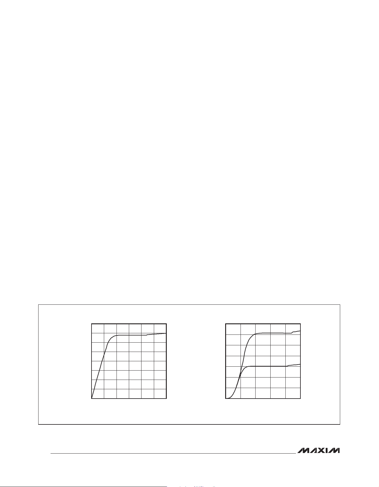
Figure 16 shows the typical current sink by a King Bright
AA3020ARWC/A white LED as the LED supply voltage is
varied from 2.5V to 5.5V. The LED currents shown are for
ports programmed for 10mA and 30mA constant current,
swept over a 2.5V to 5.5V LED supply voltage range.
It can be seen that the LED forward voltage falls with
current, allowing the LED current to fall gracefully, not
abruptly, in brownout. In practice, the LED current drops
to 11mA to 12.5mA at a 3V LED supply voltage; this is
acceptable performance at end-of-life in many backlight
applications.
Output-Level Translation
The open-drain output architecture allows the ports to level
translate the outputs to higher or lower voltages than the
MAX6948B supply (VDD). Use an external pullup resistor on
any output to convert the high-impedance, logic-high condition to a positive voltage level. Connect the resistor to any
voltage up to 5.5V. When using a pullup on a constant-current output, select the resistor value to sink no more than
a few hundred FA in logic-low condition. This ensures
that the current-sink output saturates close to GND.
For interfacing CMOS inputs, a pullup resistor value of
220kI is a good starting point. Use a lower resistance
to improve noise immunity in applications where power
consumption is less critical, or where a faster rise time is
needed for a given capacitive load.
Using Stagger with Fewer Ports
The stagger option, when selected, applies to all ports
configured as constant-current outputs. The PWM cycles
are separated to six evenly spaced start positions
(Figure 3). Optimize phasing when using some of the
ports as constant-current outputs by allocating the ports
with the most appropriate start positions. In general,
choose the ports that spread the PWM start positions as
evenly as possible. This optimally spreads out the current demand from the ports’ load supply.
Generating a Shutdown/Run Output
3.3
3.2
3.1
3.0
(V)
2.9
LED
V
2.8
2.7
2.6
2.5
2.5 5.5
Figure 16. LED Brownout
26
V
vs. V
LED
V
LED
SUPPLY
LED
SUPPLY (V)
35
30
25
20
(mA)
LED
I
15
10
5
5.04.53.0 3.5 4.0
0
2.5 5.0
I
vs. V
V
LED
SUPPLY
LED
SUPPLY (V)
4.54.03.53.0
LED
Page 27

High-Efficiency PWM LED Driver with Boost
Converter and Five Constant-Current GPIO Ports
The MAX6948B can use an I/O port to automatically generate a shutdown/run output. The shutdown/run output is
active-low when the MAX6948B is in run mode, hold-off,
ramp-down, or ramp-up, and goes high automatically
when the device finally enters shutdown after rampdown. Programming the port’s output register to value
0x02 puts the output into static constant-current mode
(Table 7). Program the port’s output current to half current (Table 9) to minimize operating current. Connect a
220kI pullup resistor to this port.
In run mode, the output port goes low, approaching 0V,
as the port’s static constant current saturates trying to
sink a higher current than the 220kI pullup resistor can
source.
In shutdown mode, the output goes high impedance
together with any other constant-current outputs. This
output remains low during ramp-up and ramp-down
sequences because the current drawn by the 220kI
pullup resistor is much smaller than the available output
constant current, even at the lowest fade-current step.
Driving Load Currents Higher than 30mA
The MAX6948B can drive loads needing more than
30mA, like high-current white LEDs, by paralleling outputs. For example, consider a white LED that requires
90mA. Drive this LED using the ports P0–P4 connected
in parallel (shorted together). Configure all of the five
ports for full current (2 x 30mA + 3 x 10mA) to meet the
90mA requirement. Control the five ports simultaneously
with one write access using register 0x0C (Table 1).
Note that because the output ports are current limiting,
they do not need to switch simultaneously to ensure safe
current sharing.
Power-Supply Considerations
V+ operates with a 2.7V to 5.5V power-supply voltage.
Bypass V+ to GND with a 2.2FF or higher ceramic
capacitor as close as possible to the device. VDD operates with a 1.7V to V+ power-supply voltage. Bypass
VDD to GND with a 0.1FF or higher ceramic capacitor as
close as possible to the device.
PCB Layout Considerations
Due to fast switching waveforms and high-current paths,
careful PCB layout is required. Minimize trace lengths
between the IC and the inductor, the diode, the input
capacitor, and the output capacitor. Minimize trace
lengths between the input and output capacitors and
the MAX6948B GND terminal, and place input and
output capacitor grounds as close together as possible. Use separate power-ground and analog-ground
copper areas, and connect them together at the outputcapacitor ground. Keep traces short, direct, and wide.
Keep noisy traces, such as the LX node trace, away from
sensitive analog circuitry. For improved thermal performance, maximize copper area of the LX and PGND
traces. Refer to the MAX6948B EV kit data sheet for an
example layout.
MAX6948B
27
Page 28

High-Efficiency PWM LED Driver with Boost
Converter and Five Constant-Current GPIO Ports
Chip Information
PROCESS: BiCMOS
MAX6948B
Package Information
For the latest package outline information and land patterns, go to www.maxim-ic.com/packages. Note that
a “+”, “#”, or “-” in the package code indicates RoHS
status only. Package drawings may show a different suffix character, but the drawing pertains to the package
regardless of RoHS status.
PACKAGE TYPE PACKAGE CODE DOCUMENT NO.
25 WLP B9-7 W252D2+1
21-0453
Maxim cannot assume responsibility for use of any circuitry other than circuitry entirely embodied in a Maxim product. No circuit patent licenses are implied.
Maxim reserves the right to change the circuitry and specifications without notice at any time.
28 Maxim Integrated Products, 120 San Gabriel Drive, Sunnyvale, CA 94086 408-737-7600
©
2009 Maxim Integrated Products Maxim is a registered trademark of Maxim Integrated Products, Inc.
 Loading...