

Page 1
General Description
The MAX6921/MAX6931 are 20-output, 76V, vacuumfluorescent display (VFD) tube drivers that interface a
multiplexed VFD tube to a VFD controller, such as the
MAX6850–MAX6853, or to a microcontroller. The
MAX6921/MAX6931 are also ideal for driving static VFD
tubes or telecom relays.
Data is input using an industry standard 4-wire serial
interface (CLOCK, DATA, LOAD, BLANK), compatibile
with either Maxim’s or industry-standard VFD driver and
controller.
For easy display control, the active-high BLANK input
forces all driver outputs low, turning the display off, and
automatically puts the MAX6921/MAX6931 into shutdown mode. Display intensity may also be controlled by
directly pulse-width modulating the BLANK input.
The MAX6921 has a serial interface data output, DOUT,
allowing any number of devices to be cascaded on the
same serial interface.
The MAX6931 has a negative supply voltage input, VSS,
allowing the drivers’ output swing to be made bipolar to
simplify filament biasing in many applications.
The MAX6921 is available in 28-pin TSSOP, SO, and
PLCC packages. The MAX6931 is available in a 28-pin
TSSOP package.
Maxim also offers 12-output VFD drivers (MAX6920) and
32-output VFD drivers (MAX6922/MAX6932).
Applications
White Goods Industrial Weighing
Gaming Machines Security
Automotive Telecom
Avionics VFD Modules
Instrumentation Industrial Control
Features
♦ 5MHz Industry-Standard 4-Wire Serial Interface
♦ 3V to 5.5V Logic Supply Range
♦ 8V to 76V Grid/Anode Supply Range
♦ -11V to 0V Filament Bias Supply (MAX6931 Only)
♦ Push-Pull CMOS High-Voltage Outputs
♦ Outputs can Source 40mA, Sink 4mA
Continuously
♦ Outputs can Source 75mA Repetitive Pulses
♦ Outputs can be Paralleled for Higher Current Drive
♦ Any Output can be Used as a Grid or an Anode
Driver
♦ Blank Input Simplifies PWM Intensity Control
♦ Small 28-Pin TSSOP Package
♦ -40°C to +125°C Temperature Range
MAX6921/MAX6931
20-Output, 76V, Serial-Interfaced
VFD Tube Drivers
________________________________________________________________ Maxim Integrated Products 1
Ordering Information
19-3020; Rev 0; 10/03
For pricing, delivery, and ordering information, please contact Maxim/Dallas Direct! at
1-888-629-4642, or visit Maxim’s website at www.maxim-ic.com.
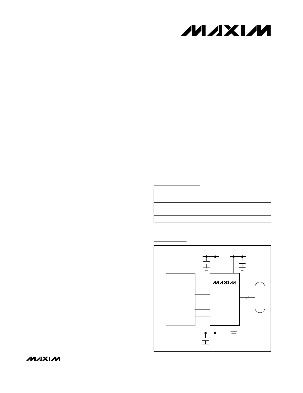
Typical Operating Circuit
Pin Configurations appear at end of data sheet.
PART TEMP RANGE PIN-PACKAGE
MAX6921AUI -40°C to +125°C 28 TSSOP
MAX6921AWI -40°C to +125°C 28 Wide SO
MAX6921AQI -40°C to +125°C 28 PLCC
MAX6931AUI -40°C to +125°C 28 TSSOP
µC
VFDOUT
VFLOAD
VFBLANK
VFCLK
100nF
100nF
+5V
C1
7
V
CC
MAX6931
6
DIN
22
CLK
23
LOAD
20
BLANK
V
SS
921
-7V
C3
8
V
BB
OUT0–OUT19
GND
+60V
C2
100nF
20
VFD TUBE
Page 2
MAX6921/MAX6931
20-Output, 76V, Serial-Interfaced
VFD Tube Drivers
2 _______________________________________________________________________________________
ABSOLUTE MAXIMUM RATINGS
ELECTRICAL CHARACTERISTICS
(Typical Operating Circuit, VBB= 8V to 76V, VCC= 3V to 5.5V, VSS= -11V to 0V, VBB- VSS≤ 76V, TA= T
MIN
to T
MAX
, unless other-
wise noted.) (Note 1)
Stresses beyond those listed under “Absolute Maximum Ratings” may cause permanent damage to the device. These are stress ratings only, and functional
operation of the device at these or any other conditions beyond those indicated in the operational sections of the specifications is not implied. Exposure to
absolute maximum rating conditions for extended periods may affect device reliability.
Voltage (with respect to GND)
V
BB
.........................................................................-0.3V to +80V
V
CC
...........................................................................-0.3V to +6V
V
SS
(MAX6931 only) ...............................................-12V to +0.3V
V
BB
- VSS(MAX6931 only) .....................................-0.3V to +80V
OUT_ (MAX6921 only) ..................(GND - -0.3V) to (V
BB
+ 0.3V)
OUT_ (MAX6931 only) ....................(V
SS
- -0.3V) to (VBB+ 0.3V)
All Other Pins..............................................-0.3V to (V
CC
+ 0.3V)
OUT_ Continuous Source Current ....................................-45mA
OUT_ Pulsed (1ms max, 1/4 max duty) Source Current ...-80mA
Total OUT_ Continuous Source Current .........................-540mA
Total OUT_ Continuous Sink Current .................................90mA
Total OUT_ Pulsed (1ms max, 1/4 max duty)
Source Current ...........................................................-960mA
OUT_ Sink Current .............................................................15mA
CLK, DIN, LOAD, BLANK, DOUT Current .......................±10mA
Continuous Power Dissipation (T
A
= +70°C)
28-Pin TSSOP (derate 12.8mW/°C
over +70°C)................................................................1025mW
28-Pin Wide SO (derate 12.5mW/°C
over +70°C)................................................................1000mW
28-Pin PLCC (derate 10.5mW/°C
over +70°C)..................................................................842mW
Operating Temperature Range
(T
MIN
to T
MAX
) ...............................................-40°C to +125°C
Junction Temperature......................................................+150°C
Storage Temperature Range .............................-65°C to +150°C
Lead Temperature (soldering, 10s) .................................+300°C
Logic Supply Voltage V
Tube Supply Voltage V
Bias Supply Voltage
(MAX6931 Only)
Total Supply Voltage
(MAX6931 Only)
Logic Supply Operating Current I
Tube Supply Operating Current I
Bias Supply Operating Current
(MAX6931 Only)
High-Voltage OUT_ V
PARAMETER SYMBOL CONDITIONS MIN TYP MAX UNITS
CC
BB
V
SS
V
- V
BB
SS
All outputs OUT_ low,
CLK = idle
CC
All outputs OUT_ high,
CLK = idle
All outputs OUT_ low
BB
All outputs OUT_ high
All outputs OUT_ low
I
SS
All outputs OUT_ high
VBB ≥ 15V
= -25mA
I
OUT
VBB ≥ 15V
H
I
= -40mA
OUT
8V < VBB < 15V
= -25mA
I
OUT
3 5.5 V
876V
-11 0 V
76 V
TA = +25°C 78 170
T
= -40°C to +125°C 200
A
TA = +25°C 540 900
T
= -40°C to +125°C 1000
A
TA = +25°C 1.65 3.0
T
= -40°C to +125°C 6.9
A
TA = +25°C 0.85 1.3
T
= -40°C to +125°C 1.4
A
TA = +25°C -0.8 -0.38
T
= -40°C to +125°C -1.9
A
TA = +25°C -1.4 -0.87
T
= -40°C to +125°C -1.5
A
TA = +25°CV
BB
- 1.1
TA = -40°C to +85°CVBB - 2
T
= -40°C to +125°CVBB - 2.5
A
TA = -40°C to +85°CVBB - 3.5
= -40°C to +125°CVBB - 4.0
T
A
TA = +25°CV
BB
- 1.2
TA = -40°C to +85°CVBB - 2.5
T
= -40°C to +125°CVBB - 3.0
A
µA
mA
mA
V
Page 3
MAX6921/MAX6931
20-Output, 76V, Serial-Interfaced
VFD Tube Drivers
_______________________________________________________________________________________ 3
ELECTRICAL CHARACTERISTICS (continued)
(Typical Operating Circuit, VBB= 8V to 76V, VCC= 3V to 5.5V, VSS= -11V to 0V, VBB- VSS≤ 76V, TA= T
MIN
to T
MAX
, unless other-
wise noted.) (Note 1)
Low-Voltage OUT_
(MAX6921 Only)
Low-Voltage OUT_
(MAX6931 Only)
Rise Time OUT_ (20% to 80%) t
Fall Time OUT_ (80% to 20%) t
SERIAL INTERFACE TIMING CHARACTERISTICS
LOAD Rising to OUT_ Falling
Delay
LOAD Rising to OUT_ Rising
Delay
BLANK Rising to OUT_ Falling
Delay
BLANK Falling to OUT_ Rising
Delay
Input Leakage Current
CLK, DIN, LOAD, BLANK
Logic-High Input Voltage
CLK, DIN, LOAD, BLANK
Logic-Low Input Voltage
CLK, DIN, LOAD, BLANK
Hysteresis Voltage
DIN, CLK, LOAD, BLANK
High-Voltage DOUT V
Low-Voltage DOUT V
PARAMETER SYMBOL CONDITIONS MIN TYP MAX UNITS
VBB ≥ 15V
I
= 1mA
OUT
V
L
8V < VBB < 15V
= 1mA
I
OUT
VBB ≥ 15V
I
= 1mA
OUT
V
L
8V < VBB < 15V
= 1mA
I
OUT
VBB = 60V, CL = 50pF, RL =2.3kΩ 0.9 2 µs
R
= 60V, C
V
F
BB
L
TA = +25°C 0.75 1
TA = -40°C to +85°C 1.5
T
= -40°C to +125°C 1.9
A
TA = +25°C 0.8 1.1
TA = -40°C to +85°C 1.6
T
= -40°C to +125°C 2.0
A
TA = +25°CV
SS
TA = -40°C to +85°CV
T
= -40°C to +125°CV
A
TA = +25°CV
SS
TA = -40°C to +85°CV
T
= -40°C to +125°CV
A
= 50pF, RL =2.3kΩ 0.6 1.5 µs
(Notes 2, 3) 0.9 1.8 µs
(Notes 2, 3) 1.2 2.4 µs
(Notes 2, 3) 0.9 1.8 µs
(Notes 2, 3) 0.5 1.3 2.5 µs
, I
I
IH
IL
V
V
∆V
IH
IL
OH
OL
I
I
I
= -1.0mA
SOURCE
= 1.0mA 0.5 V
SINK
0.8 x
V
CC
V
CC
0.5
-
+ 0.75 VSS + 1
+ 1.5
SS
+ 1.9
SS
+ 0.8 VSS + 1.1
+ 1.6
SS
+ 2.0
SS
0.05 10 µA
0.3 x
V
CC
0.6 V
V
V
V
V
V
Page 4
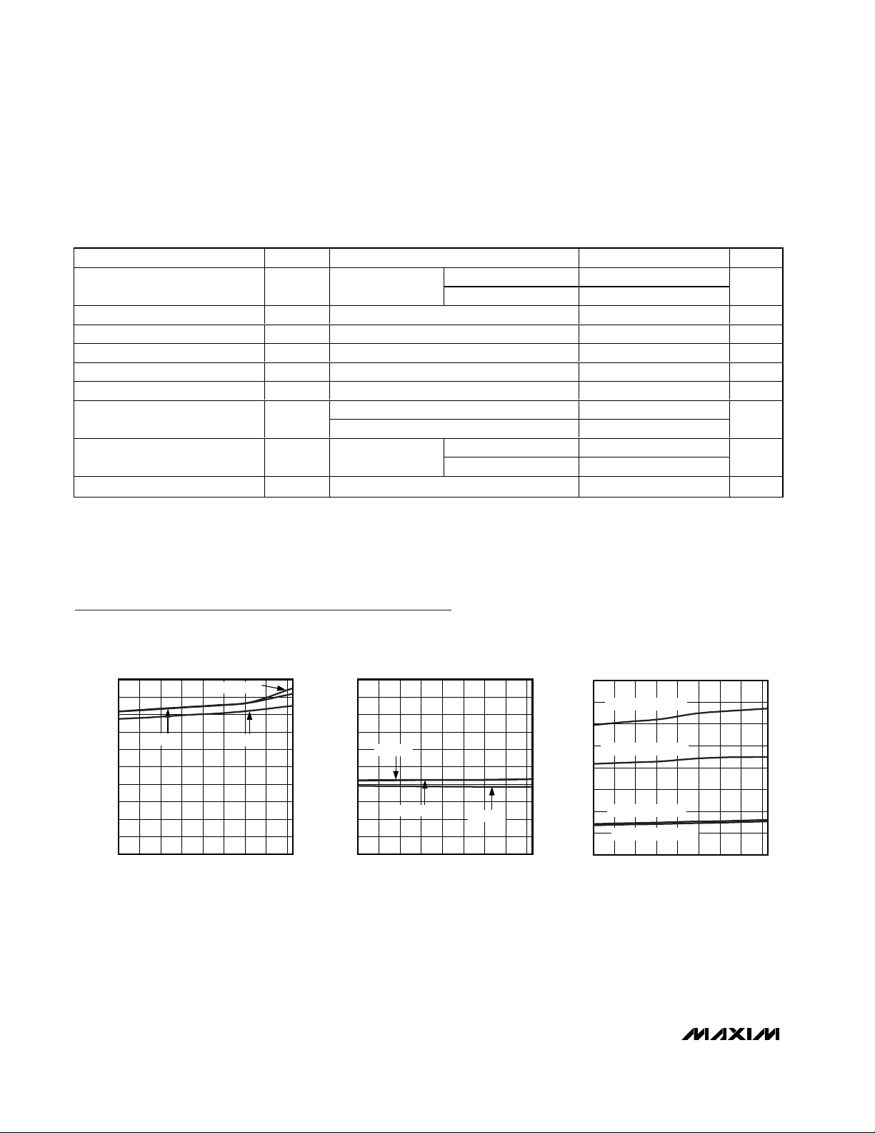
Typical Operating Characteristics
(VCC= 5.0V, VBB= 76V, and TA= +25°C, unless otherwise noted.)
MAX6921/MAX6931
20-Output, 76V, Serial-Interfaced
VFD Tube Drivers
4 _______________________________________________________________________________________
ELECTRICAL CHARACTERISTICS (continued)
(Typical Operating Circuit, VBB= 8V to 76V, VCC= 3V to 5.5V, VSS= -11V to 0V, VBB- VSS≤ 76V, TA= T
MIN
to T
MAX
, unless other-
wise noted.) (Note 1)
Note 1: All parameters are tested at TA= +25°C. Specifications over temperature are guaranteed by design.
Note 2: Guaranteed by design.
Note 3: Delay measured from control edge to when output OUT_ changes by 1V.
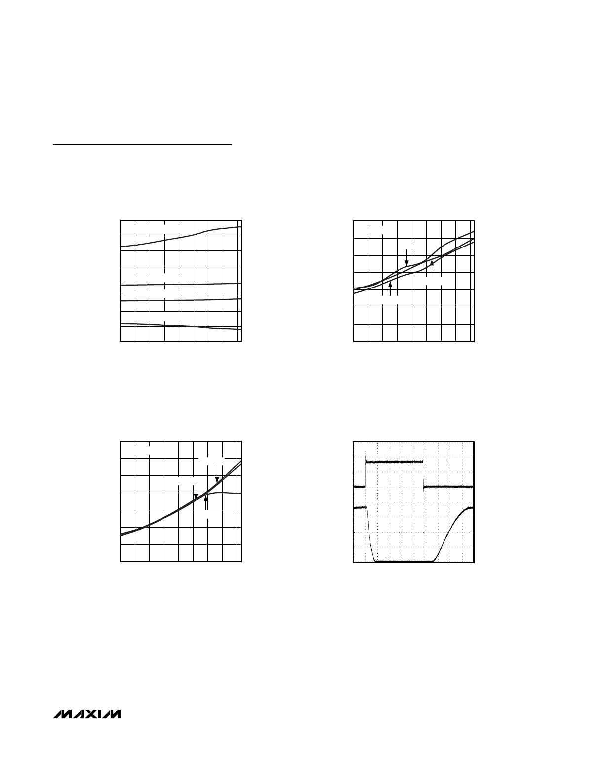
TUBE SUPPLY CURRENT (IBB)
vs. TEMPERATURE (OUTPUTS LOW)
MAX6921/31 toc01
TEMPERATURE (°C)
SUPPLY CURRENT (mA)
1008040 60020-20
0.2
0.4
0.6
0.8
1.0
1.2
1.4
1.6
1.8
2.0
0
-40 120
VBB = 76V
VBB = 40V
VBB = 8V
TUBE SUPPLY CURRENT (IBB)
vs. TEMPERATURE (OUTPUTS HIGH)
MAX6921/31 toc02
TEMPERATURE (°C)
SUPPLY CURRENT (mA)
1008040 60020-20
0.2
0.4
0.6
0.8
1.0
1.2
1.4
1.6
1.8
2.0
0
-40 120
VBB = 76V
VBB = 40V
VBB = 8V
LOGIC SUPPLY CURRENT (ICC)
vs. TEMPERATURE (OUTPUTS LOW)
MAX6921/31 toc03
TEMPERATURE (°C)
SUPPLY CURRENT (µA)
1008040 60020-20
50
100
150
200
250
300
350
400
0
-40 120
VCC = 5V, CLK = 5MHz
VCC = 3.3V, CLK = 5MHz
VCC = 5V, CLK = IDLE
VCC = 3.3V, CLK = IDLE
Rise and Fall Time DOUT
CLK Clock Period t
CLK Pulse-Width High t
CLK Pulse-Width Low t
CLK Rise to LOAD Rise Hold t
DIN Setup Time t
DIN Hold Time t
DOUT Propagation Delay t
LOAD Pulse High t
PARAMETER SYMBOL CONDITIONS MIN TYP MAX UNITS
3V to 4.5V 60 100
4.5V to 5.5V 30 80
200 ns
3.0V to 4.5V 25 120 240
4.5V to 5.5V 20 75 150
CP
CH
CL
CSH
DS
DH
DO
CSW
C
= 10pF
DOUT
(Note 2)
(Note 2) 100 ns
3.0V to 4.5V 20
4.5V to 5.5V 15
C
= 10pF
DOUT
ns
90 ns
90 ns
5ns
ns
ns
55 ns
Page 5
MAX6921/MAX6931
20-Output, 76V, Serial-Interfaced
VFD Tube Drivers
_______________________________________________________________________________________ 5
Typical Operating Characteristics (continued)
(VCC= 5.0V, VBB= 76V, and TA= +25°C, unless otherwise noted.)
LOGIC SUPPLY CURRENT (ICC)
vs. TEMPERATURE (OUTPUTS HIGH)
MAX6921/31 toc04
TEMPERATURE (°C)
SUPPLY CURRENT (µA)
1008040 60020-20
450
500
550
600
650
700
750
800
400
-40 120
VCC = 5V, CLK = 5MHz
VCC = 3.3V, CLK = 5MHz
VCC = 5V, CLK = IDLE
VCC = 3.3V, CLK = IDLE
OUTPUT VOLTAGE (VBB - VH)
vs. TEMPERATURE (OUTPUT HIGH)
MAX6921/31 toc05
TEMPERATURE (°C)
OUTPUT VOLTAGE (V)
1008040 60020-20
0.5
1.0
1.5
2.0
2.5
3.0
3.5
0
-40 120
VBB = 76V
VBB = 40V
VBB = 8V
I
OUT
= -40mA
OUTPUT VOLTAGE
vs. TEMPERATURE (OUTPUT LOW)
MAX6921/31 toc06
TEMPERATURE (°C)
OUTPUT VOLTAGE (V)
1008040 60020-20
2
4
6
8
10
12
14
0
-40 120
VBB = 40V
VBB = 8V
VBB = 76V
I
OUT
= 4mA
OUTPUT RISE AND FALL WAVEFORM
1µs/div
MAX6921/31 toc07
BLANK
2V/div
OUT_
20V/div
Page 6

MAX6921/MAX6931
20-Output, 76V, Serial-Interfaced
VFD Tube Drivers
6 _______________________________________________________________________________________
Pin Description
Figure 1. MAX6921/MAX6931 Functional Diagram
PIN
TSSOP
MAX6931 MAX6921
1–5, 10–19,
24–28
—
— 9 2 DOUT
6 6 27 DIN
7 7 28 V
88 1VBBVFD Tube Supply Voltage
9 ——V
——
1–5, 10–19,
24–28
WIDE SO/
PLCC
3–12,
17–26
NAME FUNCTION
OUT0 to
OUT19
OUT0 to
OUT19
CC
SS
20 20 13 BLANK
21 21 14 GND Ground
22 22 15 CLK
23 23 16 LOAD
VFD Anode and Grid Drivers. OUT0 to OUT19 are push-pull outputs swinging
from V
VFD Anode and Grid Drivers. OUT0 to OUT19 are push-pull outputs swinging
from V
Serial-Clock Output. Data is clocked out of the internal shift-register to DOUT
on CLK’s rising edge.
Serial-Data Input. Data is loaded into the internal shift register on CLK’s rising
edge.
Logic Supply Voltage
Filament Bias Supply Voltage
Blanking Input. High forces outputs OUT0 to OUT19 low, without altering the
contents of the output latches. Low enables outputs OUT0 to OUT19 to follow
the state of the output latches.
Serial-Clock Input. Data is loaded into the internal shift register on CLK’s
rising edge.
Load Input. Data is loaded transparently from the internal shift register to the
output latch while LOAD is high. Data is latched into the output latch on
LOAD's rising edge, and retained while LOAD is low.
to VSS.
BB
to GND.
BB
CLK
MAX6921 ONLY
DIN
LOAD
BLANK
SERIAL-TO-PARALLEL SHIFT REGISTER
OUT0 OUT1 OUT2
LATCHES
OUT19
DOUT
MAX6921
MAX6931
Page 7

Detailed Description
The MAX6921/MAX6931 are VFD tube drivers comprising a 4-wire serial interface driving 20 high-voltage Railto-Railoutput ports. The driver is suitable for both static
and multiplexed displays.
The output ports feature high current-sourcing capability to drive current into grids and anodes of static or
multiplex VFDs. The ports also have active current sinking for fast discharge of capacitive display electrodes
in multiplexing applications.
The 4-wire serial interface comprises a 20-bit shift register and a 20-bit transparent latch. The shift register is
written through a clock input CLK and a data input DIN.
For the MAX6921, the data propagates to a data output
DOUT. The data output allows multiple drivers to be
cascaded and operated together. The output latch is
transparent to the shift register outputs when LOAD is
high, and latches the current state on the falling edge
of LOAD.
Each driver output is a slew-rated controlled CMOS
push-pull switch driving between VBBand GND
(MAX6921) or VSS(MAX6931). The output rise time is
always slower than the output fall time to avoid shootthrough currents during output transitions. The output
slew rates are slow enough to minimize EMI, yet are
fast enough so as not to impact the typical 100µs digit
multiplex period and affect the display intensity.
Initial Power-Up and Operation
An internal reset circuit clears the internal registers of
the MAX6921/MAX6931 on power-up. All outputs OUT0
to OUT19 and the interface output DOUT (MAX6921
only) initialize low regardless of the initial logic levels of
the CLK, DIN, BLANK, and LOAD inputs.
4-Wire Serial Interface
The MAX6921/MAX6931 use 4-wire serial interface with
three inputs (DIN, CLK, LOAD) and a data output
(DOUT, MAX6921 only). This interface is used to write
output data to the MAX6921/MAX6931 (Figure 4) (Table
1). The serial interface data word length is 20 bits,
D0–D19.
The functions of the four serial interface pins are:
• CLK input is the interface clock, which shifts data
into the MAX6921/MAX6931s’ 20-bit shift register on
its rising edge.
• LOAD input passes data from the MAX6921/
MAX6931s’ 20-bit shift register to the 20-bit output
latch when LOAD is high (transparent latch), and
latches the data on LOAD’s falling edge
• DIN is the interface data input, and must be stable
when it is sampled on the rising edge of CLK.
• DOUT is the interface data output, which shifts data
out from the MAX6921’s 20-bit shift register on the
rising edge of CLK. Data at DIN is propagated
through the shift register and appears at DOUT (20
CLK cycles + t
DO
) later.
A fifth input, BLANK, can be taken high to force outputs
OUT0 to OUT19 low, without altering the contents of the
output latches. When the BLANK input is low, outputs
OUT0 to OUT19 follow the state of the output latches. A
common use of the BLANK input is PWM intensity control.
The BLANK input’s function is independent of the operation of the serial interface. Data can be shifted into the
serial interface shift register and latched regardless of
the state of BLANK.
MAX6921/MAX6931
20-Output, 76V, Serial-Interfaced
VFD Tube Drivers
_______________________________________________________________________________________ 7
Figure 2. MAX6921 CMOS Output Driver Structure
Figure 3. MAX6931 CMOS Output Driver Structure
Rail-to-Rail is a registered trademark of Nippon Motorola, Ltd.
V
BB
40Ω
SLEW-RATE
CONTROL
TYPICAL
OUT_
750Ω
TYPICAL
V
BB
40Ω
SLEW-RATE
CONTROL
TYPICAL
750Ω
TYPICAL
V
SS
OUT_
Page 8

MAX6921/MAX6931
Writing Device Registers Using the
4-Wire Serial Interface
The MAX6921/MAX6931 are normally written using the
following sequence:
1) Take CLK low.
2) Clock 20 bits of data in order D19 first to D0 last
into DIN, observing the data setup and hold times.
3) Load the 20 output latches with a falling edge
on LOAD.
LOAD may be high or low during a transmission. If
LOAD is high, then the data shifted into the shift register at DIN appear at the OUT0 to OUT19 outputs.
CLK and DIN may be used to transmit data to other
peripherals. Activity on CLK always shifts data into the
MAX6921/MAX6931s’ shift register. However, the
MAX6921/MAX6931 only update their output latch on
the rising edge of LOAD, and the last 20 bits of data
are loaded. Therefore, multiple devices can share CLK
and DIN, as long as they have unique LOAD controls.
Determining Driver Output Voltage Drop
The outputs are CMOS drivers, and have a resistive
characteristic. The typical and maximum sink and
source output resistances can be calculated from the
VHand VLelectrical characteristics. Use this calculated
resistance to determine the output voltage drop at different output currents.
20-Output, 76V, Serial-Interfaced
VFD Tube Drivers
8 _______________________________________________________________________________________
Figure 4. 4-Wire Serial Interface Timing Diagram
Table 1. 4-Wire Serial Interface Truth Table
L = Low logic level.
H = High logic level.
X = Don’t care.
P = Present state (shift register).
R = Previous state (latched).
LOAD
t
t
CL
CH
t
CP
t
CSW
t
CSH
CLK
DIN
DOUT
t
DH
t
DS
D19 D18 D1 D0
SERIAL
DATA
INPUT
CLOCK
INPUT
DIN
H H R0 R1 … Rn-2 Rn-1
L L R0 R1 … Rn-2 Rn-1
XR0R1R2… Rn-1 Rn
SHIFT REGISTER CONTENTS
CLK D0 D1 D2 … Dn-1 Dn LOAD D0 D1 D2 … Dn-1 Dn BLANK D0 D1 D2 … Dn-1 Dn
XXX… XX LR0R1R2… Rn-1 Rn
P0 P1 P2 … Pn-1 Pn H P0 P1 P2 … Pn-1 Pn L P0 P1 P2 … Pn-1 Pn
LOAD
INPUT
t
DO
D19
LATCH CONTENTS
XXX… XX H LLL… LL
BLANKING
INPUT
OUTPUT CONTENTS
Page 9

Output Current Ratings
The continuous current-source capability is 40mA per
output. Outputs may drive up to 75mA as a repetitive
peak current, subject to the on-time (output high) being
no longer than 1ms, and the duty cycle being such that
the output power dissipation is no more than the dissipation for the continuous case. The repetitive peak rating
allows outputs to drive a higher current in multiplex grid
driver applications, where only one grid is on at a time,
and the multiplex time per grid is no more than 1ms.
Since dissipation is proportional to current squared, the
maximum current that can be delivered for a given multiplex ratio is given by:
I
PEAK
= (grids x 1600)
1/2
mA
where grids is the number of grids in a multiplexed
display.
This means that a duplex application (two grids) can use
a repetitive peak current of 56.5mA, a triplex (three grids)
application can use a repetitive peak current of 69.2mA,
and higher multiplex ratios are limited to 75mA.
Paralleling Outputs
Any number of outputs within the same package may
be paralleled in order to raise the current drive or
reduce the output resistance. Only parallel outputs
directly (by shorting outputs together) if the interface
control can be guaranteed to set the outputs to the
same level. Although the sink output is relatively weak
(typically 750Ω), that resistance is low enough to dissipate 530mW when shorted to an opposite level output
at a VBBvoltage of only 20V. A safe way to parallel outputs is to use diodes to prevent the outputs from sinking current (Figure 5). Because the outputs cannot sink
current from the VFD tube, an external discharge resistor, R, is required. For static tubes, R can be a large
value such as 100kΩ. For multiplexed tubes, the value
of the resistor can be determined by the load capacitance and timing characteristics required. Resistor R
discharges tube capacitance C to 10% of the initial
voltage in 2.3 x RC seconds. So, for example, a 15kΩ
value for R discharges 100pF tube grid or anode from
40V to 4V in 3.5µs, but draws an additional 2.7mA from
the driver when either output is high.
Power Dissipation
Take care to ensure that the maximum package dissipation ratings for the chosen package are not exceeded. Over-dissipation is unlikely to be an issue when
driving static tubes, but the peak currents are usually
higher for multiplexed tubes. When using multiple driver devices, try to share the average dissipation evenly
between the drivers.
Determine the power dissipation (PD) for the
MAX6921/MAX6931 for static tube drivers with the following equation:
PD= (VCCx ICC) + (VBBx IBB) + ((VBB- VH) x
I
ANODE
x A))
where:
A = number of anodes driven (the MAX6921/MAX6931
can drive a maximum of 20).
I
ANODE
= maximum anode current.
(VBB- VH) is the output voltage drop at the given maximum anode current I
OUT
.
A static tube dissipation example follows:
VCC= 5V ±5%, VBB= 10V to 18V, A = 20, I
OUT
= 2mA
PD = (5.25V x 1mA)+ (18V x 1.4mA) +
((2.5V x 2mA/25mA) x 2mA x 20) = 38mW
Determine the power dissipation (PD) for the MAX6921/
MAX6931 for multiplex tube drivers with the following
equation:
PD= (VCCx ICC) + (VBBx IBB) + ((VBB- VH) x
I
ANODE
x A) + ((VBB- VH) x I
GRID
))
where:
A = number of anodes driven.
G = number of grids driven.
I
ANODE
= maximum anode current.
I
GRID
= maximum grid current.
The calculation presumes all anodes are on, but only
one grid is on. The calculated PDis the worst case,
presuming one digit is always being driven with all its
anodes lit. Actual PDcan be estimated by multiplying
this PDfigure by the actual tube drive duty cycle, taking
into account interdigit blanking and any PWM intensity
control.
MAX6921/MAX6931
20-Output, 76V, Serial-Interfaced
VFD Tube Drivers
_______________________________________________________________________________________ 9
Figure 5. Paralleling Outputs
MAX6921
MAX6931
OUT0
OUT1
D1
OUTPUT
D2
R
Page 10

MAX6921/MAX6931
A multiplexed tube dissipation example follows:
VCC= 5V ±5%, VBB= 36V to 42V, A = 12, G = 8,
I
ANODE
= 0.4mA, I
GRID
= 24mA
PD= (5.25V x 1mA)+ (42V x 1.4mA) +
((2.5V x 0.4mA/25mA) x 0.4mA x 12) +
((2.5V x 24mA/25mA) x 24mA) = 122mW
Thus, for a 28-pin wide TSSOP package (TJA= 1 / 0.0128
= 78.125°C/W from Absolute Maximum Ratings), the
maximum allowed ambient temperature TAis given by:
T
J(MAX)
= TA+ (PDx TJA) = 150°C = TA+ (0.122 x
78.125°C/W)
So TA= +140.5°C.
This means that the driver can be operated in this
application up to the MAX6921/MAX6931s’ +125°C
maximum operating temperature.
Power-Supply Considerations
The MAX6921/MAX6931 operate with multiple powersupply voltages. Bypass the VCC, VBB, and V
SS
(MAX6931 only) power-supply pins to GND with 0.1µF
capacitors close to the device. The MAX6931 may be
operated with VSStied to GND if a negative bias supply
is not required. For multiplex applications, it may be
necessary to add an additional bulk electrolytic capacitor of 1µF or greater to the VBBsupply.
Power-Supply Sequencing
The order of the power-supply sequencing is not important. The MAX6921/MAX6931 will not be damaged if
any combination of V
CC
, VBB, and VSS(MAX6931 only)
is grounded while the other supply or supplies are
maintained up to their maximum ratings. However, as
with any CMOS device, do not drive the MAX6921/
MAX6931s’ logic inputs if the logic supply V
CC
is not
operational because the input protection diodes clamp
the signals.
Cascading Drivers (MAX6921 Only)
Multiple MAX6921s may be cascaded, as shown in the
Typical Application Circuit, by connecting each driver’s
DOUT to DIN of the next drivers. Devices may be cascaded at the full 5MHz CLK speed when VCC≥ 4.5V.
When VCC<4.5V, the longer propagation delay (tDO)
limits the maximum cascaded CLK to 4MHz.
20-Output, 76V, Serial-Interfaced
VFD Tube Drivers
10 ______________________________________________________________________________________
Typical Application Circuit
Chip Information
TRANSISTOR COUNT: 2743
PROCESS: BiCMOS
MAX685x
VFDOUT
VFCLK
VFLOAD
VFBLANK DOUT
MAX6921
DIN
CLK
LOAD
BLANK
MAX6921
DIN
CLK
LOAD
BLANK DOUT
MAX6921
DIN
CLK
LOAD
BLANK DOUT
VFD TUBE
Page 11

MAX6921/MAX6931
20-Output, 76V, Serial-Interfaced
VFD Tube Drivers
______________________________________________________________________________________ 11
Pin Configurations
TOP VIEW
V
DOUT
OUT19
OUT18
OUT17
OUT16
OUT15
OUT14
OUT13
OUT12
OUT11
OUT10
BLANK
GND
BB
1
2
3
4
5
6
7
8
9
10
11
12
13
14
1
OUT4
OUT3
OUT2
OUT1
OUT0
DIN
V
V
DOUT
OUT19
OUT18
OUT17
OUT16
OUT15
2
3
4
5
6
7
CC
8
BB
9
10
11
12
13
14
MAX6921AWI
28
V
CC
27
DIN
26
OUT0
25
OUT1
24
OUT2
23
OUT3
22
OUT4
21
OUT5
20
OUT6
19
OUT7
18
OUT8
17
OUT9
16
LOAD
15
CLK
SO TSSOP
OUT18
MAX6921AUI
OUT19
DOUT
1234262728
BBVCC
V
OUT5
28
OUT6
27
OUT7
26
OUT8
25
OUT9
24
LOAD
23
CLK
22
GND
21
BLANK
20
OUT10
19
OUT11
18
OUT12
17
OUT13
16
OUT14
15
OUT4
OUT3
OUT2
OUT1
OUT0
DIN
V
V
V
OUT19
OUT18
OUT17
OUT16
OUT15
CC
BB
SS
1
2
3
4
5
6
7
8
9
10
11
12
13
14
MAX6931AUI
TSSOP
DIN
OUT0
OUT5
28
OUT6
27
OUT7
26
OUT8
25
OUT9
24
LOAD
23
CLK
22
GND
21
BLANK
20
OUT10
19
OUT11
18
OUT12
17
OUT13
16
OUT14
15
OUT8
OUT1
25
OUT2
24
OUT3
23
OUT4
22
21
OUT5
OUT6
20
OUT7
19
OUT17
OUT16
OUT15
OUT14
OUT13
OUT12
OUT11
5
6
7
8
9
10
11
MAX6921AQI
12 13 14 15 16 17 18
OUT10
BLANK
GND
CLK
LOAD
OUT9
PLCC
Page 12

MAX6921/MAX6931
20-Output, 76V, Serial-Interfaced
VFD Tube Drivers
12 ______________________________________________________________________________________
Package Information
(The package drawing(s) in this data sheet may not reflect the most current specifications. For the latest package outline information,
go to www.maxim-ic.com/packages
.)
TSSOP4.40mm.EPS
Page 13

MAX6921/MAX6931
20-Output, 76V, Serial-Interfaced
VFD Tube Drivers
______________________________________________________________________________________ 13
Package Information (continued)
(The package drawing(s) in this data sheet may not reflect the most current specifications. For the latest package outline information,
go to www.maxim-ic.com/packages
.)
N
1
TOP VIEW
D
e
FRONT VIEW
INCHES
MIN
DIM
0.093A
0.004
A1
0.014
B
0.009
C
H
E
A
B
A1
C
L
e 0.050 1.27
0.291
E
H 0.4190.394 10.00 10.65
0.016L
VARIATIONS:
INCHES
MINDIM
D
0.398 0.413 AA10.5010.10 16
D
0.447 0.463 AB11.7511.35 18
D 0.6140.598 15.20 2415.60 AD
D 0.7130.697 17.70 2818.10 AE
0-8
SIDE VIEW
MAX
0.104
0.012
0.019
0.013
0.299
0.050
MAX
0.5120.496D
MILLIMETERS
MAX
MIN
2.65
2.35
0.30
0.10
0.49
0.35
0.23
0.32
7.40 7.60
0.40 1.27
MILLIMETERS
MAX
MIN
12.60 13.00
SOICW.EPS
N MS013
20 AC
PROPRIETARY INFORMATION
TITLE:
PACKAGE OUTLINE, .300" SOIC
REV.DOCUMENT CONTROL NO.APPROVAL
21-0042
1
B
1
Page 14

MAX6921/MAX6931
20-Output, 76V, Serial-Interfaced
VFD Tube Drivers
Maxim cannot assume responsibility for use of any circuitry other than circuitry entirely embodied in a Maxim product. No circuit patent licenses are
implied. Maxim reserves the right to change the circuitry and specifications without notice at any time.
14 ____________________Maxim Integrated Products, 120 San Gabriel Drive, Sunnyvale, CA 94086 408-737-7600
© 2003 Maxim Integrated Products Printed USA is a registered trademark of Maxim Integrated Products.
Package Information (continued)
(The package drawing(s) in this data sheet may not reflect the most current specifications. For the latest package outline information,
go to www.maxim-ic.com/packages
.)
e
D3D1D
N
D3
D1
A
A1
D
B1
B
A3
D2
C
NOTES:
1. D1 DOES NOT INCLUDE MOLD FLASH.
2. MOLD FLASH OR PROTRUSIONS NOT TO EXCEED
.20mm (.008") PER SIDE.
3. LEADS TO BE COPLANAR WITHIN .10mm.
4. CONTROLLING DIMENSION: MILLIMETER
5. MEETS JEDEC MO047-XX AS SHOWN IN TABLE.
6. N = NUMBER OF PINS.
A2
A 0.165
A2
0.145
A3
0.020
B
0.013
B1
0.026
C
0.009
e
INCHES
MIN
0.050
MAX
0.180
0.1200.090A1
0.156
---
0.021
0.032
0.011
MIN
4.20
2.29
3.69
0.51
0.33
0.66
0.23
1.27
MAX
4.57
3.04
3.96
---
0.53
0.81
0.28
INCHES
MIN
MAX
0.385
D
D1D20.350
D
D1
D2
D3
D
D1
D2
D3
D
D1
D2
D
D1
D2 0.890 0.930
PROPRIETARY INFORMATION
TITLE:
0.395
0.356
0.290
0.330
REFD3 0.200
0.495
0.485
0.456
0.450
0.430
0.390
REF
0.300
0.695
0.685
0.650
0.656
0.590
0.630
REF
0.500
0.785
0.795
0.750
0.756
0.690
0.730
0.995
0.985
0.950
0.958
REF REF
FAMILY PACKAGE OUTLINE:
20L, 28L, 44L, 52L, 68L PLCC
MIN
9.78
8.89
7.37
5.08
12.32
11.43
9.91
7.62
17.40
16.51
14.99
12.70
19.94
19.05
17.53
25.02
24.13
22.61
20.320.800D3
21-0049
MAX
10.03
9.04
8.38
REF
12.57
11.58
10.92
REF
17.65
16.66
16.00
REF
20.19
19.20
18.54
REFREFD3 0.600 15.24
25.27
24.33
23.62
PLCC.EPS
N
AA
20
AB
28
AC
44
AD
52
AE
68
REV.DOCUMENT CONTROL NO.APPROVAL
1
D
1
 Loading...