

Page 1
General Description
The MAX6901 3-wire serial interface real-time clock in a
TDFN package contains a real-time clock/calendar and
31 x 8 bits of static RAM (SRAM). The real-time
clock/calendar provides seconds, minutes, hours, day,
date, month, year, and century information. A
time/date-programmable polled ALARM is included in
the MAX6901. The end of the month date is automatically adjusted for months with fewer than 31 days,
including corrections for leap year up to the year 2100.
The clock operates in either the 24hr or 12hr format
with an AM/PM indicator. A push-pull 32kHz output is
also included. The MAX6901 operates with a supply
voltage of +2V to +5.5V, is available in the ultra-small 8pin TDFN package, and works over the industrial temperature range, -40°C to +85°C.
Applications
Point-of-Sale Equipment
Intelligent Instruments
Fax Machines
Battery-Powered Products
Portable Instruments
Features
♦ Real-Time Clock Counts Seconds, Minutes,
Hours, Day of Week, Date of Month, Month, Year,
and Century
♦ Leap-Year Compensation Valid up to Year 2100
♦ Wide +2V to +5.5V Operating Voltage Range
♦ 3-Wire Serial Interface, 2MHz at 5V, 500kHz at 2V
♦ 31 x 8-Bit SRAM for Scratchpad Data Storage
♦ Uses Standard 32.768kHz, 12.5pF Watch Crystal
♦ Low Timekeeping Current (400nA at 2V)
♦ Single-Byte or Multiple-Byte (Burst Mode)
Data Transfer for Read or Write of Clock
Registers or SRAM
♦ 8-Pin 3mm x 3mm x 0.8mm TDFN
Surface-Mount Package
♦ Push-Pull 32.768kHz Clock Output
♦ Programmable Time/Date Polled ALARM Function
♦ No External Crystal Bias Resistors or Capacitors
Required
MAX6901
3-Wire Serial RTC in a TDFN
________________________________________________________________ Maxim Integrated Products 1
19-2085; Rev 1; 2/03
Ordering Information
Related Real-Time Clock Products
Pin Configuration appears at end of data sheet.
Functional Diagram appears at end of data sheet.
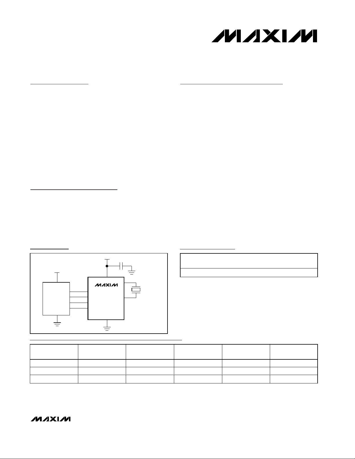
µC
0.1µF
32.768kHz
CRYSTAL
1
4
3
6
2
5
3.3V
3.3V
MAX6901
7
8
P1.0
CLKIN
P1.1
P1.2
SCLK
CS
I/O
32KHZ
GND
V
CC
X1
X2
Typical Operating Circuit
For pricing, delivery, and ordering information, please contact Maxim/Dallas Direct! at
1-888-629-4642, or visit Maxim’s website at www.maxim-ic.com.
I2C is a trademark of Philips Corp. Purchase of I2C components of Maxim Integrated Products, Inc., or one of its sublicensed Associated
Companies, conveys a license under the Philips I
2
C Patent rights to use these components in an I2C system provided that the system
conforms to the I
2
C Standard Specification as defined by Philips.
SPI is a trademark of Motorola, Inc.
PART
MAX6901ETA-T -40°C to +85°C 8 TDFN AGV
ALARM
FUNCTION
PART
MAX6900 I2C™ compatible 31 x 8 ——6 TDFN
MAX6901 3 wire 31 x 8 Polled 32kHz 8 TDFN
MAX6902 SPI™ compatible 31 x 8 Polled — 8 TDFN
INTERFACE
SERIAL
ALARM
(bits)
TEMP
RANGE
OUTPUT
FREQUENCY
PINPACKAGE
PIN-PACKAGE
TOP
MARK
Page 2
MAX6901
3-Wire Serial RTC in a TDFN
2 _______________________________________________________________________________________
ABSOLUTE MAXIMUM RATINGS
Stresses beyond those listed under “Absolute Maximum Ratings” may cause permanent damage to the device. These are stress ratings only, and functional
operation of the device at these or any other conditions beyond those indicated in the operational sections of the specifications is not implied. Exposure to
absolute maximum rating conditions for extended periods may affect device reliability.
VCCto GND.......................................................……-0.3V to +6V
All Other Pins to GND ................................-0.3V to (Vcc + 0.3V)
Current into Any Pin..........................................................±20mA
Rate-of-Rise, V
CC
............................................................100V/µs
Continuous Power Dissipation (T
A
= +70°C)
8-Pin TDFN (derate 24.4mW/°C above +70°C).........1951.0mW
Junction Temperature .....................................................+150°C
Storage Temperature Range .............................-65°C to +150°C
ESD Protection (all pins, Human Body Model) ..................2000V
Lead Temperature (soldering, 10s) .................................+300°C
DC ELECTRICAL CHARACTERISTICS
(VCC= +2.0V to +5.5V, TA= -40°C to +85°C, unless otherwise noted. Typical values are at VCC= +3.3V, TA= +25°C.) (Note 1)
PARAMETER SYMBOL CONDITIONS MIN TYP MAX UNITS
Operating Voltage Range V
Active Supply Current (Note 2) I
Timekeeping Supply Current
(Note 3)
32kHz OUTPUT
Output High Voltage (Note 5) V
Output Low Voltage (Note 5) V
Duty Cycle 40 %
Output Leakage Current VIN = 0 to VCC, 32kHz output disabled -10 10 nA
3-WIRE DIGITAL INPUTS AND OUTPUTS (SCLK, I/O, CS)
Input High Voltage V
Input Low Voltage V
Input Leakage Current VIN = 0 to V
SCLK, RST Capacitance 5pF
I/O Capacitance 10 pF
I/O Output Low Voltage V
I/O Output High Voltage V
I
CC
CC
TK
OH
OL
OL
OH
VCC = +2.0V 0°C < TA < +70°C 110
VCC = +5V 0°C < TA < +70°C 800
VCC = +2.0V 0.4 0.7
VCC = +5V 1.3 1.7
VCC = +2.0V, I
VCC = +5.0V, I
VCC = +2.0V, I
VCC = +5.0V, I
VCC = +2.0V 1.4
IH
VCC = +5.0V 2.2
VCC = +2.0V 0.6
IL
VCC = +5.0V 0.8
CC
VCC = +2.0V, I
VCC = +5.0V, I
VCC = +2.0V, I
VCC = +5.0V, I
2 5.5 V
= -0.4mA 1.8
SOURCE
= -1mA 4.5
SOURCE
= 1.5mA 0.4
SINK
= 4mA 0.4
SINK
-10 10 nA
= 1.5mA 0.4
SINK
= 4mA 0.4
SINK
= -0.4mA 1.8
SOURCE
= -1mA 4.5
SOURCE
µA
µA
V
V
V
V
V
V
Page 3
MAX6901
3-Wire Serial RTC in a TDFN
_______________________________________________________________________________________ 3
Note 1: All parameters are 100% tested at TA= +25°C. Limits over temperature are guaranteed by design and not production tested.
Note 2: I
CC
is specified with the I/O grounded, CS high, SCLK = 2MHz at VCC= +5V; SCLK = 500kHz at VCC= +2.0V, 32kHz output
enabled, and no load on 32kHz output.
Note 3: Timekeeping current is specified with CS = GND, SCLK = GND, I/O = GND, 32kHz = GND, and 32kHz disabled.
Note 4: All values referred to V
IH
min and VILmax levels.
Note 5: Guaranteed by design. Not production tested.
AC ELECTRICAL CHARACTERISTICS
(VCC= +2.0V to +5.5V, TA= -40°C to +85°C, unless otherwise noted. Typical values are at VCC= +3.3V, TA= +25°C.) (Figures 4, 5
and Notes 1, 4)
OSCILLATOR
X1 to Ground Capacitance (Note 5) 25 pF
X2 to Ground Capacitance (Note 5) 25 pF
3-WIRE SERIAL TIMING
Data to CLK Setup t
CLK to Data Hold t
CLK to Data Delay t
CLK Low Time t
CLK High Time t
CLK Frequency f
CLK Rise and Fall Time tR, t
CS to CLK Setup t
CLK to CS Hold t
CS Inactive Time t
CS to I/O High Z t
SCLK to I/O High Z t
PARAMETER SYMBOL CONDITIONS MIN TYP MAX UNITS
DC
CDH
CDD
CL
CH
CLK
CC
CCH
CWH
CDZ
CCZ
VCC = +2V 200
VCC = +5V 50
VCC = +2V 280
VCC = +5V 70
CL = 50pF
VCC = +2V 1000
VCC = +5V 250
VCC = +2V 1000
VCC = +5V 250
VCC = +2V DC 0.5
VCC = +5V DC 2.0
VCC = +2V 2000
F
VCC = +5V 500
VCC = +2V 4
VCC = +5V 1
VCC = +2V 240
VCC = +5V 60
VCC = +2V 4
VCC = +5V 1
RL = 1kΩ, CL = 60pF
RL = 1kΩ, CL = 60pF
VCC = +2V 800
V
= +5V 200
CC
VCC = +2V 0 280
= +5V 0 70
V
CC
VCC = +2V 0 280
V
= +5V 0 70
CC
ns
ns
ns
ns
ns
MHz
ns
µs
ns
µs
ns
ns
Page 4
MAX6901
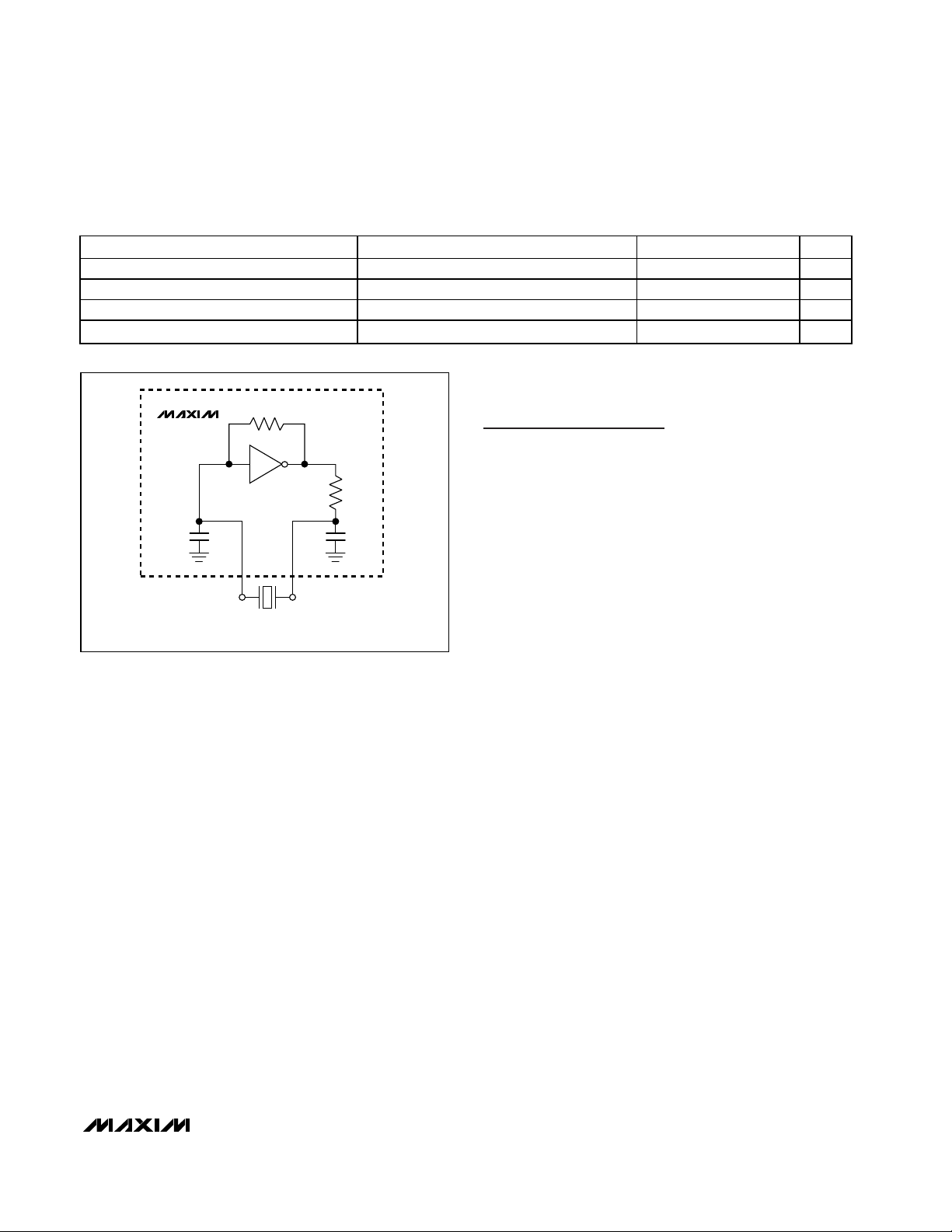
Detailed Description
The MAX6901 is a real-time clock/calendar with a 3-wire
serial interface and 31 ✕8 bits of SRAM. It provides seconds, minutes, hours, day of the week, date of the
month, month, and year information, held in seven 8-bit
timekeeping registers (Functional Diagram). An on-chip
32.768kHz oscillator circuit does not require any external resistors or capacitors to operate. Table 1 specifies
the parameters for the external crystal, and Figure 1
shows a functional schematic of the oscillator circuit.
The MAX6901’s register addresses and definitions are
described in Tables 2 and 3. Time and calendar data
are stored in the registers in binary coded decimal
(BCD) format. A polled alarm function is included for
scheduled timing of user-defined times or intervals.
Command and Control
Address/Command Byte
Each data transfer into or out of the MAX6901 is initiated by an Address/Command byte. The Address/
Command byte specifies which registers are to be
accessed, and if the access is a read or a write. Table
2 shows the Address/Command bytes and their associated registers, and Table 3 lists the hex codes for all
read and write operations. The Address/Command
bytes are input LSB (bit 0) first. Bit 0 specifies a write
(logic 0) or read (logic 1). Bits 1 to 5 specify the designated register to be written or read. Bit 6 specifies register data (logic 0), or RAM data (logic 1). The MSB (bit
7) must be logic 1. If the MSB is a zero, writes to the
MAX6901 are disabled.
3-Wire Serial RTC in a TDFN
4 _______________________________________________________________________________________
Typical Operating Characteristics
(TA = +25°C, unless otherwise noted.)
0.1
2.0 2.5 3.5 4.0 5.54.5 5.03.0
TIMEKEEPING CURRENT
vs. SUPPLY VOLTAGE
1.0
10.0
MAX6901 toc01
SUPPLY VOLTAGE (V)
SUPPLY CURRENT (µA)
Pin Description
PIN NAME FUNCTION
1 SCLK Serial Clock Input. 3-wire serial clock for I/O data transfers.
2VCCPower-Supply Pin. Bypass VCC to GND with a 0.1µF capacitor.
3 X2 External 32.768kHz Crystal Connection
4 X1 External 32.768kHz Crystal Connection
5 32KHZ
6 GND Ground Connection
7 CS Chip-Select Input. Active-high for valid data transfers.
8 I/O Data Input/Output. 3-wire serial data input/output connection.
— PAD Ground
Buffered Push-Pull 32.768kHz Output. When enabled, 32KHZ puts a buffered version of the timekeeping clock.
When disabled, 32KHZ is high impedance. The power-on reset (POR) default state of 32KHZ is enabled.
Page 5
Clock Burst Mode
Accessing the Clock Burst register specifies burstmode operation. In this mode, multiple bytes are read
or written with a single Address/Command write. If the
Clock Burst register is accessed (BEh for Write and
BFh for Read), the first seven clock/calendar registers
(Seconds, Minutes, Hours, Date, Month, Day, and Year)
and the Control register, are consecutively read or written, starting with the LSB of the Seconds register. When
writing to the clock registers in burst mode, all seven
registers must be written in order for the data to be
transferred (see Example: Setting the Clock with a
Burst Write).
RAM Burst Mode
Sending the RAM Burst Address/Command specifies
Burst-Mode operation. In this mode, the 31 RAM registers can be consecutively read or written, starting with
bit 0 of address C0h for Writes, and C1h for Reads.
Burst Read outputs all 31 registers of RAM. When writing to RAM in burst mode, it is not necessary to write all
31 bytes for the data to transfer; each complete byte
written is transferred to RAM. When reading from RAM,
data bits are output until all 31 bytes have been read,
or until CS is driven low.
Setting the Clock
Writing to the Timekeeping Registers
The Time and Date are set by writing to the timekeeping registers (Seconds, Minutes, Hours, Date, Month,
Day, Year, and Century). During a write operation, an
input buffer accepts the new time data while the timekeeping registers continue to increment normally,
based on the crystal counter. The buffer also keeps the
timekeeping registers from changing as the result of an
incomplete Write operation, and collision detection circuitry ensures that a time write does not occur coincident with a Seconds register increment. The updated
time data are loaded into the timekeeping registers on
the falling edge of CS, at the end of the 3-wire serial
Write operation. An incomplete Write operation aborts
the update procedure, and the contents of the input
buffer are discarded. The timekeeping registers reflect
the new time, beginning with the first Seconds register
increment after the falling edge of CS.
Although both Single Writes and Burst Writes are possible, the best way to write to the timekeeping registers is
with a Burst Write. With a Burst Write, main timekeeping
registers (Seconds, Minutes, Hours, Date, Month, Day,
Year), and the Control register are written sequentially
following the Address/Command byte. They must be
written as a group of eight registers, with 8 bits each,
for proper execution of the Burst Write function. All
seven timekeeping registers are simultaneously loaded
into the clock counters by the falling edge of CS, at the
end of the 3-wire serial Write operation. For a normal
burst data transfer, the worst-case error that can occur
between the actual time and the written time update is
1 second.
If Single Write operations are used to enter data into the
timekeeping registers, error checking is required. If the
Seconds register is not to be written, then begin by
reading the Seconds register and save it as initial-seconds. Write to the required timekeeping registers and
MAX6901
3-Wire Serial RTC in a TDFN
_______________________________________________________________________________________ 5
Figure 1. Oscillator Circuit Schematic
Table 1. Acceptable Quartz Crystal Parameters
Frequency f
Equivalent Series Resistance (ESR) R
Parallel Load Capacitance C
Q Factor Q
PARAMETER SYMBOL MIN TYP MAX UNITS
Rf
MAX6901
Rd
25pF
Cg
X1 X2
EXTERNAL
CRYSTAL
Cd
25pF
32.76
s
L
40 60 kΩ
11.2 12.5 13.7 pF
40,000 60,000
kHz
Page 6
MAX6901
then read the Seconds register again (final-seconds).
Check to see that final-seconds is equal to initial-seconds. If not, repeat the write process. If the Seconds
register is to be written, update the Seconds register
first, and then read it back and store its value (initialseconds). Update the remaining timekeeping registers
and then read the Seconds register again (final-sec-
3-Wire Serial RTC in a TDFN
6 _______________________________________________________________________________________
Table 2. Register Address/Definition
FUNCTION A7 A6 A5 A4 A3 A2 A1 A0 VALUE D7 D6 D5 D4 D3 D2 D1 D0
TIMEKEEPING
SECOND
REGISTER ADDRESS REGISTER DEFINITION
1000 000
MINUTE
HOUR
DATE
MONTH
1000 001
1000 010
1000 011
1000 100
RD
/W
RD
/W
RD
/W
RD
/W
RD
/W
00-59
*POR STATE 0 0 0 0 0000
00-59
*POR STATE
00-23 12/24
01-12 1/0
*POR STATE 0 0 0 00000
01-28/29
01-30
01-31
*POR STATE
01-12 0 0 0 10M 1 MONTH
*POR STATE
32kHz
EN
ALM
OUT
10 SEC 1 SEC
10 MIN 1 MIN
0 0000000
10
HR
A/P
0/1
10
HR
1 HR
0
0 0 10 DATE 1 DATE
0 0 000001
0 0 0 00001
DAY
1000 101
YEAR
CONTROL
CENTURY
Note: *POR STATE
1000 110
1000 111
1001 001
defines power-on reset state of register content.
RD
/W
RD
/W
RD
/W
RD
/W
*POR STATE 0
*POR STATE 0 0 0 1 1 0 0 1
01-07 0 0 0 0 0 WEEKDAY
*POR STATE
00-99 10 YEAR 1 YEAR
*POR STATE 0 1 1 1 0 0 0 0
00-99 1000 YEAR 100 YEAR
0 0 0 0 0 00 1
WP 0 0 0 0 0 0 0
0 0 0 0 0 0 0
Page 7

MAX6901
3-Wire Serial RTC in a TDFN
_______________________________________________________________________________________ 7
Table 2. Register Address/Definition (continued)
FUNCTION A7 A6 A5 A4 A3 A2 A1 A0 VALUE D7 D6 D5 D4 D3 D2 D1 D0
ALARM
CONFIG
RESERVED 0 0 0 0 0 1 1 1
Do not write
to this location.
ALARM
THRESHOLDS
SECOND
MINUTE
HOUR
REGISTER ADDRESS REGISTER DEFINITION
1001 010
1001 011
1001 100
1001 101
1001 110
RD
/W
RD
/W
RD
/W
RD
/W
RD
/W
*POR STATE 0
*POR STATE
00-59
*POR STATE 0 1 1 1 1111
00-59 0 10 MIN 1 MIN
*POR STATE
00-23 12/24
01-12 1/0
*POR STATE 1 0 1 11111
0
00000111
0 10 SEC 1 SEC
0 1111111
DAY
YEAR
0 0 0 0 0 0 0
0
10
HR
A/P
0/1
MONTH
10
HR
DATE
HOUR
1 HR
MINUTE
SECOND
DATE
MONTH
YEAR
CLOCK
BURST
Note: *POR STATE
1001 111
1010 000
DAY
1010 001
1010 010
1011 111
01-28/29
RD
/W
RD
/W
RD
/W
RD
/W
RD
/W
defines power-on reset state of register content.
01-30
01-31
*POR STATE
01-12 0 0 0 10 M 1 MONTH
*POR STATE
01-07 0 0 0 0 0 WEEKDAY
*POR STATE
00-99 10 YEAR 1 YEAR
*POR STATE 1 1 1 1 1111
0 0 10 DATE 1 DATE
0 0 111111
0 0 0 11111
0 0 0 0 0 11 1
Page 8
MAX6901
onds). Check to see that final-seconds is equal to initial-seconds. If not, repeat the write process.
Note: After writing to any time or date register, no read
or write operations are allowed for 45µs.
AM/PM and 12Hr/24Hr Mode
Bit 7 of the Hours register selects 12hr or 24hr mode.
When high, 12hr mode is selected. In 12hr mode, bit 5 is
the AM/PM bit, logic high for PM. In 24hr mode, bit 5 is
the second 10hr bit, logic high for hours 20 through 23.
Write-Protect Bit
Bit 7 of the Control register is the write-protect bit.
When high, the write-protect bit prevents write operations to all registers except itself. After initial settings
are written to the timekeeping registers, set the writeprotect bit to logic 1 to prevent erroneous data from
entering the registers during power glitches or interrupted serial transfers. The lower 7 bits (bits 0–6) are
unusable, and always read zero. Any data written to
bits 0–6 are ignored. Bit 7 must be set to zero before a
single byte write to the clock, before a write to RAM, or
during a burst write to the clock.
Example: Setting the Clock
with a Burst Write
To set the clock with a Burst Write operation to
10:11:31PM, Thursday July 4th, 2002, write BEh as
Address/Command byte, followed by 8 bytes, B1h,
11h, B0h, 04h, 07h, 04h, 02h, and 00h (Table 2). BEh
accesses the Clock Burst Write register. The first byte,
B1h, sets the Seconds register to 31, and disables the
32.768kHz output. The second byte, 11h, sets the
Minutes register to 11. The third byte, B0h, sets the
Hours register to 12hr mode, and 10PM. The fourth
byte, 04h, sets the Date register (day of the month) to
the 4th. The fifth byte, 07h, sets the Month register to
July. The sixth byte, 04h, sets the Day register (day of
the week) to Thursday. The seventh byte, 02h, sets the
Year register to 02. The eighth byte, 00h, clears the
write-protect bit of the Control register to allow writing to
the MAX6901. The Century register is not accessed
with a Burst Write and therefore must be written to separately to set the century to 20. Note the Century register corresponds to the thousand and hundred digits of
the current year and defaults to 19.
Reading the Clock
Reading the Timekeeping Registers
The main timekeeping registers (Seconds, Minutes,
Hours, Date, Month, Day, Year) can be read with either
Single Reads or a Burst Read. In the MAX6901, a latch
buffers each clock counter’s data. Clock counter data
are latched by the 3-wire serial Read command (on the
falling edge of SCLK, after the Address/Command byte
has been sent by the Master to read a timekeeping register). Collision-detection circuitry ensures that this
3-Wire Serial RTC in a TDFN
8 _______________________________________________________________________________________
Table 2. Register Address/Definition (continued)
FUNCTION A7 A6 A5 A4 A3 A2 A1 A0 VALUE D7 D6 D5 D4 D3 D2 D1 D0
RAM
RAM 0 1100000
RAM 30 1111110
RAM BURST 1111111
Note: *POR STATE defines power-on reset state of register content.
REGISTER ADDRESS REGISTER DEFINITION
RD
/W
••
••
••
RD
/W
RD
/W
RAM DATA 0 xxxxxxxx
••
••
••
RAM DATA 30 xxxxxxxx
Page 9

MAX6901
3-Wire Serial RTC in a TDFN
_______________________________________________________________________________________ 9
Table 3. HEX Register Address/Description
ADDRESS/COMMAND
WRITE
ADDRESS/COMMAND
BYTE (HEX)
80 81 SECONDS 00
82 83 MINUTES 00
84 85 HOUR 00
86 87 DATE 01
88 89 MONTH 01
8A 8B DAY 01
8C 8D YEAR 70
8E 8F CONTROL 00
90 91 RESERVED Nonapplicable
92 93 CENTURY 19
94 95 ALARM CONFIGURATION 00
96 97 RESERVED 07
98 99 SECONDS ALARM THRESHOLD 7F
9A 9B MINUTES ALARM THRESHOLD 7F
9C 9D HOURS ALARM THRESHOLD BF
9E 9F DATE ALARM THRESHOLD 3F
A0 A1 MONTH ALARM THRESHOLD 1F
A2 A3 DAY ALARM THRESHOLD 07
A4 A5 YEAR ALARM THRESHOLD FF
BE BF CLOCK BURST Nonapplicable
C0 C1 RAM 0 Indeterminate
C2 C3 RAM 1 Indeterminate
C4 C5 RAM 2 Indeterminate
C6 C7 RAM 3 Indeterminate
C8 C9 RAM 4 Indeterminate
CA CB RAM 5 Indeterminate
CC CD RAM 6 Indeterminate
CE CF RAM 7 Indeterminate
D0 D1 RAM 8 Indeterminate
D2 D3 RAM 9 Indeterminate
D4 D5 RAM 10 Indeterminate
D6 D7 RAM 11 Indeterminate
D8 D9 RAM 12 Indeterminate
DA DB RAM 13 Indeterminate
DC DD RAM 14 Indeterminate
DE DF RAM 15 Indeterminate
E0 E1 RAM 16 Indeterminate
E2 E3 RAM 17 Indeterminate
READ
BYTE (HEX)
DESCRIPTION
POR CONTENTS
(HEX)
Page 10

MAX6901
does not happen coincident with a Seconds counter
increment to ensure accurate time data is being read.
The clock counters continue to count and keep accurate time during the Read operation.
The simplest way to read the timekeeping registers is to
use a Burst Read. In a Burst Read, the main timekeeping registers (Seconds, Minutes, Hours, Date, Month,
Day, Year) and the Control register are read sequentially in the order listed with the Seconds register first.
They are read out as a group of eight registers, with 8
bits each. All timekeeping registers (except Century)
are latched upon the receipt of the Burst Read command. The worst-case error between the “actual” time
and the “read” time is 1 second for a normal data transfer.
The timekeeping registers may also be read using
Single Reads. If Single Reads are used, it is necessary
to do some error checking on the receiving end,
because it is possible that the clock counters could
change during the Read operations, and report inaccurate time data. The potential for error is when the
Seconds register increments before all the registers are
read. For example, suppose a carry of 13:59:59 to
14:00:00 occurs during Single Read operations. The
net data read could be 14:59:59, which is erroneous.
To prevent errors from occurring with Single Read operations, read the Seconds register first (initial-seconds)
and store this value for future comparison. After the
remaining timekeeping registers have been read,
reread the Seconds register (final-seconds). Check that
the final-seconds value equals the initial-seconds value;
if not, repeat the entire Single Read process. Using
Single Reads at a 100kHz serial speed, it takes under
2.5ms to read all seven of the timekeeping registers,
including two reads of the Seconds register.
Example: Reading the Clock
with a Burst Read
To read the time with a Burst Read, send BFh as the
Address/Command byte. Then clock out 8 bytes,
Seconds, Minutes, Hours, Date of the month, Month,
Day of the week, Year, and finally the Control byte. All
data are output LSB first. Decode the required information based on the register definitions listed in Table 2.
Using the Alarm
A polled alarm function is available by reading the ALM
OUT bit. The ALM OUT bit is D7 of the Minutes timekeeping register. A logic 1 in ALM OUT indicates the
alarm function is triggered. There are eight registers
associated with the alarm function, seven programmable Alarm Threshold registers and one programmable
Alarm Configuration register. The Alarm Configuration
register determines which Alarm Threshold registers
are compared to the timekeeping registers, and the
ALM OUT bit sets if the compared registers are equal.
Table 2 shows the function of each bit of the Alarm
Configuration register. Placing a logic 1 in any given bit
of the Alarm Configuration register enables the respec-
3-Wire Serial RTC in a TDFN
10 ______________________________________________________________________________________
Table 3. HEX Register Address/Description (continued)
ADDRESS/COMMAND
WRITE
ADDRESS/COMMAND
BYTE (HEX)
E4 E5 RAM 18 Indeterminate
E6 E7 RAM 19 Indeterminate
E8 E9 RAM 20 Indeterminate
EA EB RAM 21 Indeterminate
EC ED RAM 22 Indeterminate
EE EF RAM 23 Indeterminate
F0 F1 RAM 24 Indeterminate
F2 F3 RAM 25 Indeterminate
F4 F5 RAM 26 Indeterminate
F6 F7 RAM 27 Indeterminate
F8 F9 RAM 28 Indeterminate
FA FB RAM 29 Indeterminate
FC FD RAM 30 Indeterminate
FE FF RAM Burst Nonapplicable
READ
BYTE (HEX)
DESCRIPTION
POR CONTENTS
(HEX)
Page 11

tive alarm function. For example, if the Alarm
Configuration register is set to 0000 0011, ALM OUT is
set when both the minutes and seconds indicated in
the Alarm Threshold registers match the respective
timekeeping registers. Once set, ALM OUT stays high
until it is cleared by reading or writing to the Alarm
Configuration register, or by reading or writing to any of
the Alarm Threshold registers. The Alarm Configuration
register is written with Address/Command 94h, and
read with Address/Command 95h.
Using the On-Board RAM
The static RAM is 31 x 8 bits addressed consecutively
in the RAM address space. Even-addressed commands (C0h–FCh) are used for Writes, and oddaddressed commands (C1h–FDh) are used for Reads.
The contents of the RAM are static and remain valid for
VCCdown to 2V. All RAM data are lost if power is
cycled. The write-protect bit (bit 7 of the Control register), when high, disallows any changes to RAM.
3-Wire Serial Interface
Interfacing the MAX6901 with a microcontroller is
accomplished by using a 3-wire, synchronous, serial
interface. Required to communicate are a Chip Select
signal (CS), a Serial Clock signal (SCLK), and a Data
line (I/O).
All data transfers are framed by the CS signal that must
be active-high for any data transfer to occur. At the
beginning of any data transfer (rising edge of CS),
SCLK should be low. This prevents the MAX6901 from
misinterpreting the transition of CS as a high-to-low
transition of SCLK (if SCLK were to be left high when
CS transitions from a low to high). The first 8 bits sent
after CS is pulled high by the microcontroller comprise
the Address/Command Byte, which tells the MAX6901
if the data transfer is a read or a write, and which register is read to or written from. Data are clocked into the
MAX6901, through the I/O pin, on the rising edges of
SCLK, and data are clocked out on the falling edge of
SCLK. Data format is always LSB first to MSB last.
When CS is low, I/O is high impedance.
Single data transfer timing is shown in Figure 2. Burstmode data transfer timing is shown in Figure 3.
Detailed Read and Write timing diagrams are shown in
Figures 4 and 5, respectively.
Chip Select
CS serves two functions. First, CS turns on the control
logic that allows access to the Shift register for
Address/Command and data transfer. Second, CS provides a method of terminating either single-byte or multiple-byte data transfers. All data transfers are initiated
by driving CS high. If CS is low, I/O is high impedance.
At power-up, CS must be low until V
CC
≥ 2.0V.
Serial Clock
A clock cycle on SCLK is a rising edge followed by a
falling edge. For data input, data must be valid at I/O
during the rising edge of the clock. For data outputs,
bits are valid on I/O after the falling edge of clock. Also,
SCLK must be low when CS is driven high.
Data Input (Single-Byte Write)
Following the eight SCLK cycles that input a SingleByte Write Address/Command, data bits are input on
the rising edges of the next eight SCLK cycles.
Additional SCLK cycles are ignored. Input data LSB first.
Data Input (Burst Write)
Following the eight SCLK cycles that input a Burst Write
Address/Command, data bits are input on the rising
edges of the following SCLK cycles. The number of
clock cycles depends on whether the timekeeping registers or RAM are being written. A clock Burst Write
requires an Address/Command byte, 7 timekeeping
data bytes, and 1 Control register byte. A Burst Write to
RAM may be terminated after any complete data byte
by driving CS low. Input data LSB first (Figures 3 and 5).
Data Output (Single-Byte Read
and Burst Read)
A read from the MAX6901 is initiated by an Address/
Command Write from the microcontroller (master) to the
MAX6901 (slave). The Address/Command Write portion
of the data transfer is clocked into the MAX6901 on rising clock edges. On the eighth rising SCLK edge, the
last bit of the Address/Command Byte is clocked into
the MAX6901. After t
CDH
(CLK to Data Hold time,
Figure 4), the microcontroller must release the data
line. On the eighth falling edge of SCLK, the MAX6901
takes control of the data line and begins to output data.
The MAX6901 outputs data on the falling edge of SCLK
after t
CDD
(CLK to Data Delay time, Figure 4). On the
next rising edge of SCLK, I/O goes to high impedance
after t
CCZ
(which is specified with a maximum time).
Minimum time for t
CCZ
can be 0ns. Since the I/O line
can go to high impedance on the rising edge of SCLK,
it is best to read the data from the MAX6901 before the
rising edge of SCLK but after t
CDD
(CLK to Data Delay
time). This is best accomplished through the microcontroller I/O port pins by writing a low to SCLK, waiting
t
CDD
(CLK to Data Delay time), reading the MAX6901
I/O pin, and then writing a high to SCLK. Data bytes are
output LSB first. Additional SCLK cycles transmit additional data bits, as long as CS remains high. This permits continuous burst-mode read capability.
MAX6901
3-Wire Serial RTC in a TDFN
______________________________________________________________________________________ 11
Page 12

MAX6901
32.768kHz Output (32KHZ)
32KHZ is a push-pull 32.768kHz output for timing or
clocking of external devices. Bit D7 in the Clock
Seconds register is the active-low enable bit for 32KHZ.
When D7 is logic 0, 32KHZ is enabled. When logic 1,
32KHZ is disabled and set to high impedance. Poweron reset enables the 32.768kHz output.
Applications Information
Crystal Selection
The MAX6901 is designed to use a standard 32.768kHz
watch crystal. Table 1 details the recommended crystal
requirements. Some suggested crystals are listed in
Table 4. In addition to the specified SMT devices, some
of the listed manufacturers also offer other package
options.
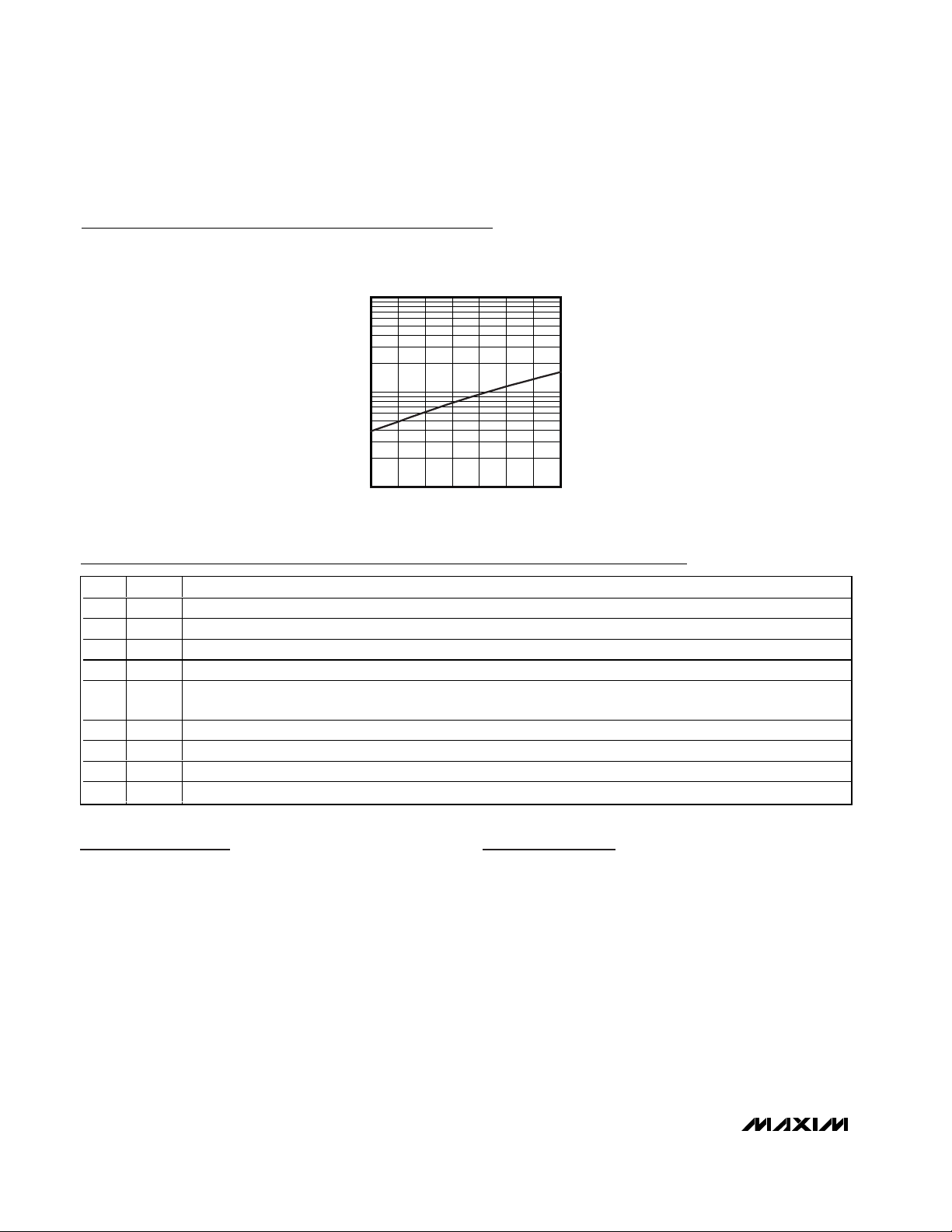
Frequency Stability and Temperature
Timekeeping accuracy of the MAX6901 is dependent
on the frequency stability of the external crystal. To
determine frequency stability, use the parabolic curve
in Figure 6 and the following equations:
∆f = fk (T
0
- T)
2
where:
∆f = change in frequency from +25°C
3-Wire Serial RTC in a TDFN
12 ______________________________________________________________________________________
Figure 2. Single Byte Data Transfer
(a) 3-WIRE SINGLE BYTE READ:
CS
SCLK
A0
I/O
A1 A2 A3 A4 A5 A6 A7
11A1 A2 A3 A4 A5 R
D0 D1 D2 D3 D4 D5 D6 D7
ADDRESS/COMMAND BYTE
R = RAM/ REGISTER SELECT BIT
RAM = 1, REGISTER = 0
(b) 3-WIRE SINGLE BYTE WRITE:
CS
SCLK
I/O
A1 A2 A3 A4 A5 A6 A7 D0 D1 D2 D3 D4 D5 D6
0
A1 A2 A3 A4 A5 R 1
ADDRESS/COMMAND BYTE
R = RAM/ REGISTER SELECT BIT
RAM = 1, REGISTER = 0
I/O DATA BYTE
D7
I/O DATA BYTE
Page 13

f = nominal crystal frequency
k = parabolic curvature constant (-0.035ppm/°C2
±0.005ppm/°C2 for 32.768kHz watch crystals)
T0= turnover temperature (+25°C ±5°C for 32.768kHz
watch crystals)
T = temperature of interest (°C)
For example: What is the worst-case change in oscillator frequency from +25°C ambient to +45°C ambient?
∆f
drift
= 32,768✕ (-0.04✕ (1✕ 10-6))✕ (20-45)
2
= -0.8192Hz
What is the worst-case timekeeping error per second?
Error due to temperature drift:
∆t
drift
= {[1 / [(f+∆f
drift
) / 32768]]-1s} / 1s
∆t
drift
= {[1 / [(32768 - 0.8192) / 32768]]-1}/1s
= 0.000025s/s
Error due to +25°C initial crystal tolerance of ±20ppm:
∆f
initial
= 32,768✕ (-20✕ ((1✕ 10-6)) = -0.65536Hz
∆t
initial
= {[1 / [(f+∆f
initial
) / 32768]]-1s} / 1s
∆t
initial
= {[1 / [(32768-0.65536) / 32768]]-1} / 1s
= 0.000025s/s
Total timekeeping error per second:
MAX6901
3-Wire Serial RTC in a TDFN
______________________________________________________________________________________ 13
Figure 3. Burst Mode Data Transfer
SCLK
()
CS
A0
I/O
(b) 3-WIRE BURST WRITE:
SCLK
I/O
A1 A2 A3 A4 A5 A6 A7
ADDRESS/COMMAND BYTE I/O DATA BYTE 1
R = RAM/ REGISTER SELECT BIT
RAM = 1, REGISTER = 0
CS
A0 A1 A2 A3 A4 A5 A6 A7 D0 D1 D2 D3 D4 D5 D6
0111 11R1
ADDRESS/COMMAND BYTE I/O DATA BYTE 1 I/O DATA BYTE N
R = RAM/ REGISTER SELECT BIT
RAM = 1, REGISTER = 0
R11 1 111 1
D1 D2
D0
D3 D4 D5
D6 D7
D7
D1 D2
D0
N = 8 FOR TIMEKEEPING REGISTER BURST
N = 31 MAX FOR RAM BURST
D0 D1 D2 D3 D4 D5 D6 D7
N = 8 FOR TIMEKEEPING REGISTER BURST
N = 31 MAX FOR RAM BURST
D3 D4 D5
I/O DATA BYTE N
D6 D7
Page 14

MAX6901
∆t
total
= ∆t
drift
+ ∆t
initial
∆t
total
= 0.00002+0.000025=0.000045s/s
After 1 month, that translates to:
Total worst-case timekeeping error at the end of 1
month at +45°C is about 120s or 2 min (assumes negligible parasitic layout capacitance).
Oscillator Start Time
The MAX6901 oscillator typically takes 5s to 10s to
begin oscillating. To ensure the oscillator is operating
correctly, the software should validate proper timekeeping. This is accomplished by reading the Seconds
register. Any reading of 1s or more from the POR value
of zero is a validation of proper startup.
Power-On Reset
The MAX6901 contains an integral POR circuit that
ensures all registers are reset to a known state on
power-up. Once VCCrises above 1.6V (typ), the POR
circuit releases the registers for normal operation. When
3-Wire Serial RTC in a TDFN
14 ______________________________________________________________________________________
Figure 4. 3-Wire Read Data Transfer Serial Timing Diagram
Figure 5. 3-Wire Write Data Transfer Serial Timing Diagram
CS
t
CC
SCLK
t
CDH
t
DC
I/O
01701
READ ADDRESS/COMMAND BYTE READ DATA BIT
CS
t
CCZ
t
CDD
t
CDD
t
CWH
t
CDZ
t
CC
SCLK
t
CDH
t
DC
I/O
∆t days
=
31 24 60 60
()
0 00045 120 528
./.
()
017 0
WRITE ADDRESS/COMMAND BYTE WRITE DATA BIT
×
ss s
hr
×
day hr
=
min
t
CL
t
CDH
s
×
min
×
t
t
R
t
F
CCH
Page 15

VCCdrops to less than 1.6V (typ), the MAX6901 resets
all register contents to the POR defaults (Table 2).
RESERVED Registers
Addresses/Commands 90h, 91h, 96h, and 97h are
reserved for factory testing ONLY. Do not write to these
registers. If inadvertent Writes are done to any of these
registers, cycle power to the MAX6901.
Power-Supply Considerations
For most applications, a 0.1µF capacitor from VCCto
GND provides adequate bypassing for the MAX6901. A
series resistor can be added to the supply line for operation in extremely harsh or noisy environments.
Timekeeping Current—Normal Operation
When I/O is high impedance (CS = low, or after each
rising-clock edge for a data output transfer), there is a
potential for increased timekeeping current (up to 100x)
if the I/O is allowed to float. If minimum timekeeping
current is desired, the microcontroller port pin should
be configured as an input with a weak pullup.
Alternatively, use a 100kΩ or less pulldown or pullup
resistor (for microcontroller port pins with ≤1µA input
leakage).
There are similar considerations for 32KHZ if it is
placed in its high-impedance state. For lowest timekeeping current, it should not be allowed to float. Force
it high or low, or terminate it with a pullup or pulldown
resistor.
Timekeeping Current—Battery Backup
Systems
Often times, an RTC is operated in a system with a
backup battery. A microprocessor supervisory circuit
with backup battery switchover, or other switching
arrangement, is used to switch power from VCCto
V
BATT
when VCCfalls below a set threshold. Most of
these systems leave only the RTC and some SRAM to
run from V
BATT
. The microcontroller that communicates
with the RTC is powered only from VCC. When the
microcontroller is reset, its port pins typically become
high impedance. This essentially floats I/O, CS, and
SCLK on the MAX6901. There is a potential for
increased timekeeping current (up to x100) as VCCfalls
through the linear region of the input gates for I/O,
SCLK, and CS. The duration of this effect depends on
the discharge rate of VCC. To minimize current draw
from V
BATT
in such systems, ensure that VCCfalls
rapidly at power down. One option is a VCCdischarge
resistor of 100kΩ or less from VCCto ground. This also
ensures sufficient impedance when VCCis gone back
through the microcontroller’s ESD protection, to keep
I/O, SCLK, and CS from floating. Alternately, a 100kΩ
pulldown (for microcontroller port pins with ≤1µA input
leakage) on each pin (I/O, SCLK, and CS) ensures that
timekeeping current specifications are met during the
power switchover.
MAX6901
3-Wire Serial RTC in a TDFN
______________________________________________________________________________________ 15
Table 4. 32.768kHz Surface-Mount Watch Crystals
Figure 6. Typical Temperature Curve for 32.768kHz Watch
Crystal
MANUFACTURER
Abracon Corporation ABS25-32.768-12.5-B-2-T -40°C to +85°C 12.5 ±20
Caliber Electronics
ECS INC International ECS-.327-12.5-17 -10°C to +60°C 12.5 ±20
Fox Electronics FSM327 -40°C to +85°C 12.5 ±20
M-tron SX2010/ SX2020 -20°C to +75°C 12.5 ±20
Raltron RSE-32.768-12.5-C-T -10°C to +60°C 12.5 ±20
SaRonix 32S12A -40°C to +85°C 12.5 ±20
-50 -40 -30 -20 -10 0 10 20 25 30 40 50 60 70 80 90
0
-50
TEMPERATURE (°C)
MANUFACTURER
PART NO.
AWS2A-32.768kHz,
TEMP. RANGE C
-20°C to +70°C 12.5 ±20
L
(pF)
+25°C FREQUENCY
TOLERANCE (ppm)
-100
∆f (ppm)
-150
-200
-250
TYPICAL TEMPERATURE CHARACTERISITICS
(k = 0.035ppm/°C
2
, TO = +25°C)
Page 16

MAX6901
There are similar considerations for 32KHZ if it is
placed in its high-impedance state. For lowest timekeeping current, it should not be allowed to float. Force
it high or low, or terminate it with a pullup or pulldown
resistor.
PC Board Layout Considerations
The MAX6901 uses a very-low-current oscillator to minimize supply current. This causes the oscillator pins, X1
and X2, to be relatively high impedance. Exercise care
to prevent unwanted noise pickup.
Connect the 32.768kHz crystal directly across X1 and
X2 of the MAX6901. To eliminate unwanted noise pickup, design the PC board using these guidelines (Figure
7): place the crystal as close to X1 and X2 as possible
and keep the trace lengths short; place a guard ring
around the crystal, X1 and X2 traces (where applicable), and connect the guard ring to GND; keep all signal traces away from beneath the crystal, X1, and X2.
Finally, an additional local ground plane can be added
under the crystal on an adjacent PC board layer. The
plane should be isolated from the regular PC board
ground plane, and tied to ground at the MAX6901
ground pin. Restrict the plane to be no larger than the
perimeter of the guard ring. Do not allow this ground
plane to contribute significant capacitance between X1
and X2.
Chip Information
TRANSISTOR COUNT: 26,214
PROCESS: CMOS
3-Wire Serial RTC in a TDFN
16 ______________________________________________________________________________________
Figure 7. Printed Circuit Board Layout for Crystal Connections
GROUND PLANE
VIA CONNECTION
V
PLANE
GUARD RING
*
CC
VIA CONNECTION
SM WATCH CRYSTAL
*
0.1µF
SM CAP
**
*
**
*
MAX6901
*
*
GROUND PLANE
VIA CONNECTION
*
**
GROUND PLANE
VIA CONNECTION
*
*
**
*
LAYER 1 TRACE
**
LAYER 2 LOCAL GROUND PLANE
CONNECT ONLY TO PIN 6
GROUND PLANE VIA
Page 17

MAX6901
3-Wire Serial RTC in a TDFN
______________________________________________________________________________________ 17
Functional Diagram
GND
32KHZX1
1
2
87I/O
CSV
CC
X2
SCLK
TDFN
TOP VIEW
6
5
MAX6901
3
4
Pin Configuration
32kHz
SCLK
V
GND
X1
X2
CS
I/O
CC
OSCILLATOR
32.768kHz
INPUT SHIFT
REGISTERS
ALARM OUT
ALARM
CONTROL
LOGIC
DIVIDER
CONTROL
LOGIC
ADDRESS
REGISTER
31 × 8
RAM
1Hz
SECONDS
MINUTES
HOURS
DATE
MONTH
DAY
YEAR
CONTROL
CENTURY
ALARM
CONFIGURATION
TEST
CONFIGURATION
ALARM
THRESHOLDS
CLOCK
BURST
RAM
BURST
Page 18

MAX6901
3-Wire Serial RTC in a TDFN
Maxim cannot assume responsibility for use of any circuitry other than circuitry entirely embodied in a Maxim product. No circuit patent licenses are
implied. Maxim reserves the right to change the circuitry and specifications without notice at any time.
18 ____________________Maxim Integrated Products, 120 San Gabriel Drive, Sunnyvale, CA 94086 408-737-7600
© 2003 Maxim Integrated Products Printed USA is a registered trademark of Maxim Integrated Products.
Package Information
(The package drawing(s) in this data sheet may not reflect the most current specifications. For the latest package outline information
go to www.maxim-ic.com/packages
.)
PIN 1
INDEX
AREA
D
E
A
A2
b
E2
DETAIL A
e
D2
C0.35
L
PIN 1 ID
1N1
[(N/2)-1] x e
REF.
6, 8, &10L, QFN THIN.EPS
A
NUMBER OF LEADS SHOWN ARE FOR REFERENCE ONLY
COMMON DIMENSIONS
MIN. MAX.
SYMBOL
0.70 0.80
A
2.90 3.10
D
E
2.90 3.10
0.00 0.05
A1
L
0.20 0.40
k
0.25 MIN.
A2 0.20 REF.
PACKAGE VARIATIONS
PKG. CODE
T633-1 1.50–0.10D22.30–0.10
N
6
1.50–0.10
E2
2.30–0.10T833-1 8
A1
L
JEDEC SPEC
0.95 BSCeMO229 / WEEA
MO229 / WEEC
0.65 BSC
C
L
e
0.40–0.05b1.90 REF
0.25–0.05 2.00 REFMO229 / WEED-30.50 BSC1.50–0.10 2.30–0.1010T1033-1
k
C
L
e
DALLAS
SEMICONDUCTOR
PROPRIETARY INFORMATION
TITLE:
PACKAGE OUTLINE, 6, 8 & 10L,
TDFN, EXPOSED PAD, 3x3x0.80 mm
APPROVAL
[(N/2)-1] x e
1.95 REF0.30–0.05
DOCUMENT CONTROL NO. REV.
21-0137 D
L
1
2
DALLAS
SEMICONDUCTOR
PROPRIETARY INFORMATION
TITLE:
PACKAGE OUTLINE, 6, 8 & 10L,
TDFN, EXPOSED PAD, 3x3x0.80 mm
DOCUMENT CONTROL NO.APPROVAL
21-0137
REV.
2
2
D
 Loading...