

Page 1
For pricing, delivery, and ordering information, please contact Maxim/Dallas Direct! at
1-888-629-4642, or visit Maxim’s website at www.maxim-ic.com.
General Description
The MAX6900, I2C™-bus-compatible real-time clock
(RTC) in a 6-pin TDFN package contains a real-time
clock/calendar and 31-byte
✕
8-bit wide of static random access memory (SRAM). The real-time clock/calendar provides seconds, minutes, hours, day, date,
month, and year information. The end of the month date
is automatically adjusted for months with fewer than 31
days, including corrections for leap year up to the year
2100. The clock operates in either the 24hr or 12hr format with an AM/PM indicator.
Applications
Portable Instruments
Point-of-Sale Equipment
Intelligent Instruments
Battery-Powered Products
Features
♦ Real-Time Clock Counts Seconds, Minutes,
Hours, Date, Month, Day, and Year
♦ Leap Year Compensation Valid up to Year 2100
♦ Fast (400kHz) I
2
C-Bus-Compatible Interface from
2.0V to 5.5V
♦ 31
✕
8 SRAM for Scratchpad Data Storage
♦ Uses Standard 32.768kHz, 12.5pF Load, Watch
Crystal
♦ Ultra-Low 225nA (typ) Timekeeping Current
♦ Single-Byte or Multiple-Byte (Burst Mode) Data
Transfer for Read or Write of Clock Registers or
SRAM
♦ 6-Pin 3mm x 3mm x 0.8mm TDFN Surface-Mount
Package
♦ No External Crystal Bias Resistors or Capacitors
Required
MAX6900
I2C-Compatible RTC in a TDFN
________________________________________________________________ Maxim Integrated Products 1
19-1942; Rev 3; 6/03
Typical Operating Circuit
X1
GNDX2
1 6 SDA
5 SCL
V
CC
MAX6900
TDFN
TOP VIEW
2
34
Pin Configuration
Ordering Information
Related Real-Time Clock Products
I2C is a trademark of Philips Corp. Purchase of I2C components
of Maxim Integrated Products, Inc., or one of its sublicensed
Associated Companies, conveys a license under the Philips I
2
C
Patent Rights to use these components in an I2C system, provided that the system conforms to the I2C Standard Specification
as defined by Philips.
SPI is a trademark of Motorola, Inc.
PART TEMP RANGE
MAX6900ETT-T -40°C to +85°C 6 TDFN AEU
PINPACKAGE
TOP
MARK
PART SERIAL BUS SRAM
ALARM
FUNCTION
OUTPUT
FREQUENCY
PIN-PACKAGE
MAX6900 I2C compatible 31 ✕ 8 ——6 TDFN
MAX6901 3-wire 31 ✕ 8 Polled 32kHz 8 TDFN
MAX6902 SPI™ compatible 31 ✕ 8 Polled — 8 TDFN
V
CC
V
CC
V
CC
µC
RPU RPU
RPU = t
r/Cbus
0.01µF
5
6
SCL
SDA
1
V
CC
MAX6900
GND
4
X1
X2
2
CRYSTAL
3
Page 2
MAX6900
I2C-Compatible RTC in a TDFN
2 _______________________________________________________________________________________
ABSOLUTE MAXIMUM RATINGS
Stresses beyond those listed under “Absolute Maximum Ratings” may cause permanent damage to the device. These are stress ratings only, and functional
operation of the device at these or any other conditions beyond those indicated in the operational sections of the specifications is not implied. Exposure to
absolute maximum rating conditions for extended periods may affect device reliability.
VCCto GND..............................................................-0.3V to +6V
All Other Pins to GND ................................-0.3V to (V
CC
+ 0.3V)
Input Current
All Pins ............................................................................20mA
Output Current
All Outputs .......................................................................20mA
Rate of Rise, V
CC
............................................................100V/µs
Continuous Power Dissipation (T
A
= +70°C)
6-Pin TDFN (derate 24.4mW/°C above +70°C) .......1951.0mW
Operating Temperature Range ...............................T
MIN
to T
MAX
MAX6900 ETT-T .......................T
MIN
= -40°C, T
MAX
= +85°C
Junction Temperature .....................................................+150°C
Storage Temperature Range ............................ -65°C to +150°C
ESD Protection (all pins, Human Body model) ..................2000V
Lead Temperature (soldering, 10s) ...…………………….+300°C
DC ELECTRICAL CHARACTERISTICS
(VCC= +2.0V to +5.5V, TA= T
MIN
to T
MAX
, unless otherwise noted. Typical values are at VCC= +3.3V, TA= +25°C.) (Note 1)
AC ELECTRICAL CHARACTERISTICS
(VCC= +2.0V to +5.5V, TA= T
MIN
to T
MAX
, unless otherwise noted. Typical values are at VCC= +3.3V, TA= +25°C.) (Notes 1, 6)
Operating Voltage Range V
Active Supply Current (Note 2) I
Timekeeping Supply Current
(Note 3)
2-WIRE DIGITAL INPUTS SCL, SDA
Input High Voltage V
Input Low Voltage V
Input Hysteresis (Note 5) V
Input Leakage Current (Note 4) 0 < VIN < V
Input Capacitance (Note 5) 10 pF
2-WIRE DIGITAL OUTPUT SDA
Output Low Voltage V
PARAMETER SYMBOL CONDITIONS MIN TYP MAX UNITS
CC
CC
I
TK
IH
IL
HYS
OL
VCC = +2.0V 30
VCC = +5.0V 110
VCC = +2.0V 0.225 0.630
VCC = +5.0V 1.2 1.7
CC
I
= 4mA 0.4 V
SINK
2 5.5 V
0.7 x V
CC
0.05 x
V
CC
-10 10 nA
0.3 x
V
CC
µA
µA
V
V
V
OSCILLATOR
X1 to Ground Capacitance 25 pF
X2 to Ground Capacitance 25 pF
FAST I2C-BUS-COMPATIBLE TIMING
SCL Clock Frequency f
Bus Free Time Between STOP
and START Condition (Note 4)
PARAMETER SYMBOL CONDITIONS MIN TYP MAX UNITS
SCL
t
BUF
0 400 kHz
1.3 µs
Page 3

MAX6900
I2C-Compatible RTC in a TDFN
_______________________________________________________________________________________ 3
AC ELECTRICAL CHARACTERISTICS (continued)
(VCC= +2.0V to +5.5V, TA= T
MIN
to T
MAX
, unless otherwise noted. Typical values are at VCC= +3.3V, TA= +25°C.) (Notes 1, 6)
Note 1: All parameters are 100% tested at TA= +25°C. Limits over temperature are guaranteed by design and not production tested.
Note 2: I
CC
is specified with SCL = 400kHz and SDA = 400kHz.
Note 3: I
TK
is specified with SCL = Logic High (4.7kΩ pullup resistor) and SDA = Logic High (4.7kΩ pullup resistor);
I
2
C-compatible bus inactive.
Note 4: MAX6900 I/O pins do not obstruct the SDA and SCL lines if V
CC
is switched off.
Note 5: Guaranteed by design. Not subject to production testing.
Note 6: All values referred to V
IH
min
and V
IL
max
levels.
Note 7: The MAX6900 internally provides a hold time of at least 300ns for the SDA signal (referred to the V
IH
min
of the SCL signal)
in order to bridge the undefined region of the falling edge of SCL.
Note 8: C
B
= total capacitance of one bus line in pF.
Note 9: The maximum t
f
for the SDA and SCL bus lines is specified at 300ns. The maximum fall time for the SDA output stage tfis
specified at 250ns. This allows series protection resistors to be connected between the SDA/SCL pins and the SDA/SCL
bus lines without exceeding the maximum specified t
f
.
PARAMETER SYMBOL CONDITIONS MIN TYP MAX UNITS
Hold Time After (Repeated)
START Condition (After this
Period, the First Clock Is
Generated)
Repeated START Condition
Setup Time
STOP Condition Setup Time t
Data Hold Time (Note 7) t
Data Setup Time t
SCL Low Period t
SCL High Period t
Minimum SCL/SDA Rise Time
(Note 8)
Maximum SCL/SDA Rise Time
(Note 8)
Minimum SCL/SDA Fall Time
(Receiving) (Notes 8, 9)
Maximum SCL/SDA Fall Time
(Receiving) (Notes 8, 9)
Minimum SDA Fall Time
(Transmitting) (Notes 8, 9)
Maximum SDA Fall Time
(Transmitting) (Notes 8, 9)
Pulse Width of Spike Suppressed t
Capacitive Load for Each
Bus Line
t
HD:STA
t
SU:STA
SU:STO
HD:DAT
SU:DAT
LOW
HIGH
t
r
t
r
t
f
t
f
t
f
t
f
SP
C
B
0.6 µs
0.6 µs
0.6 µs
0 0.9 µs
100 ns
1.3 µs
0.6 µs
20 +
0.1C
B
ns
300 ns
20 +
0.1C
B
ns
300 ns
20 +
0.1C
B
ns
250 ns
50 ns
400 pF
Page 4
Detailed Description
The MAX6900 contains eight timekeeping registers,
burst address registers, a control register, an on-chip
32.768kHz oscillator circuit, and a serial 2-wire, I2Ccompatible interface. There are also 31 bytes, 8 bits
wide of SRAM on board. Time and calendar data are
stored in the registers in a binary-coded decimal (BCD)
format. Figure 1 shows an I2C-bus-compatible timing
diagram. Figure 2 shows the MAX6900 functional diagram.
Real-Time Clock
The RTC provides seconds, minutes, hours, day, date,
month, and year information. The end of the month is
automatically adjusted for months with fewer than 31
MAX6900
I2C-Compatible RTC in a TDFN
4 _______________________________________________________________________________________
Typical Operating Characteristics
(TA = +25°C, unless otherwise noted.)
0
0.3
0.4
0.1
0.2
0.6
0.5
1.0
0.7
0.8
0.9
1.1
1.4
1.5
1.2
1.3
1.6
1.0 2.0 2.5 3.01.5 3.5 4.0 4.5 5.55.0 6.0
TIMEKEEPING CURRENT vs. V
CC
MAX6900 toc01
VCC (V)
TIMEKEEPING CURRENT (µA)
Pin Description
Figure 1. Detailed
I
2
C-Bus Timing Diagrams
PIN NAME FUNCTION
1VCCPower Supply
2 X1 32.768kHz External Crystal
3 X2 32.768kHz External Crystal
4 GND Ground
5 SCL I2C-Bus-Compatible Clock Input
6 SDA
— PAD Ground
PROTOCOL
SCL
SDA
2
I
C-Bus-Compatible Data
Input/Output
START
CONDITION
(S)
t
t
LOW
r
t
SU:STA
t
BUF
t
HD:STA
BIT 7
MSB
(A7)
t
HIGH
t
HD:DAT
BIT 6
(A6)
1/f
SCL
t
f
t
HD:DAT
BIT 0
LSB
(R/W)
ACKNOWLEDGE
(A)
t
SU:STO
STOP
CONDITION
(P)
Page 5
days, including corrections for leap year up to the year
2100.
Crystal Oscillator
The MAX6900 uses an external, standard 12.5pF load
watch crystal. No other external components are
required for this timekeeping oscillator. Power-up oscillator start-time is dependent mainly upon applied V
CC
and ambient temperature. The MAX6900, because of
its low timekeeping current, exhibits a typical startup
time between 5s to 10s.
I2C-Compatible Interface
Interfacing the MAX6900 with a microprocessor or
other I2C master is made easier by using the serial, I2Cbus-compatible or other I2C master interface. Only 2
wires are required to communicate with the clock and
SRAM: SCL (serial clock) and SDA (data line). Data is
transferred to and from the MAX6900 over the I/O data
line, SDA. The MAX6900 uses 7-bit slave ID addressing. The MAX6900 does not respond to general call
address commands.
Applications Information
I2C-Bus-Compatible Interface
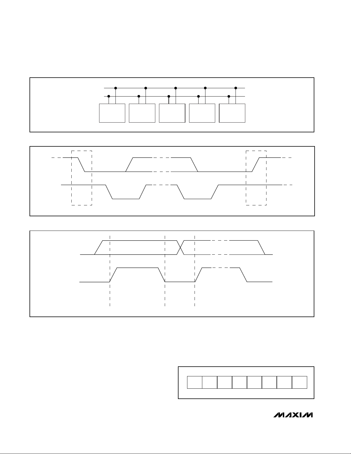
The I2C-bus-compatible serial interface allows bidirectional, 2-wire communication between multiple ICs. The
two lines are SDA and SCL. Connect both lines to a
positive supply through individual pullup resistors. A
device on the I2C-compatible bus that generates a
message is called a transmitter and a device that
receives the message is a receiver. The device that
controls the message is the master and the devices
that are controlled by the master are called slaves
(Figure 3). The word message refers to data in the form
of three 8-bit bytes for a Single Read or Write. The first
byte is the Slave ID byte, the second byte is the
Address/Command byte, and the third is the data.
Data transfer can only be initiated when the bus is not
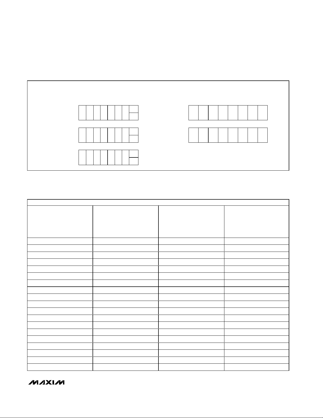
busy (both SDA and SCL are high). A high-to-low transition of SDA while SCL is high is defined as the Start
(S) condition; low-to-high transition of the data line
while SCL is high is defined as the Stop (P) condition
(Figure 4).
MAX6900
I2C-Compatible RTC in a TDFN
_______________________________________________________________________________________ 5
Figure 2. Functional Diagram
VCC
GND
SCL
SDA
ADDRESS
REGISTER
31 X 8
SRAM
1Hz
SECONDS
MINUTES
HOURS
DATE
MONTH
DAY
YEAR
CONTROL
CENTURY
CLOCK
BURST
X1
X2
OSCILLATOR
32.768kHz
2
C BUS
I
INTERFACE
DIVIDER
CONTROL
LOGIC
Page 6
MAX6900
I2C-Compatible RTC in a TDFN
6 _______________________________________________________________________________________
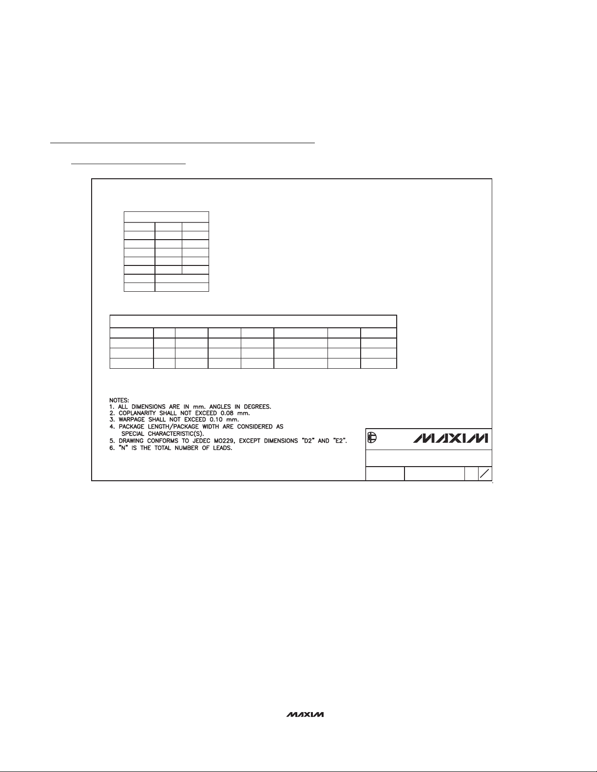
After the Start condition occurs, 1 bit of data is transferred for each clock pulse. The data on SDA must
remain stable during the high portion of the clock pulse
as changes in data during this time are interpreted as a
control signal (Figure 5). Any time a start condition
occurs, the Slave ID must follow immediately, regardless of completion of the previous data transfer.
Before any data is transmitted on the I
2
C-bus-compatible serial interface, the device that is expected to
respond is addressed first. The first byte sent after the
start (S) procedure is the Address byte or 7-bit Slave
ID. The MAX6900 acts as a slave transmitter/receiver.
Therefore, SCL is only an input clock signal and SDA is
a bidirectional data line. The Slave Address for the
MAX6900 is shown in Figure 6.
Figure 5. I2C Bus Bit Transfer
Figure 6. I2C Bus Slave Address or 7-Bit Slave ID
Figure 3. I2C Bus System Configuration
Figure 4. I2C Bus Start and Stop Conditions
SDA
SCL
SDA
SCL
S
START CONDITION STOP CONDITION
SDA
MASTER
TRANSMITTER/
RECEIVER
SLAVE
RECEIVER
SLAVE
TRANSMITTER/
RECEIVER
MASTER
TRANSMITTER
MASTER
TRANSMITTER/
RECEIVER
SDA
SCL
P
SCL
DATA LINE
STABLE;
DATA VALID
CHANGE
OF DATA
ALLOWED
RD/W
0000101
BIT 0BIT 7
Page 7

MAX6900
I2C-Compatible RTC in a TDFN
_______________________________________________________________________________________ 7
An unlimited number of data bytes between the start
and stop conditions can be sent between the transmitter and receiver. Each 8-bit byte is followed by an
acknowledge bit. Also, a master receiver must generate an acknowledge after each byte it receives that has
been clocked out of the slave transmitter.
The device that acknowledges must pull down the SDA
line during the acknowledge clock pulse (Figure 7), so
that the SDA line is stable low during the high period of
the acknowledge clock pulse (setup and hold times
must also be met). A master receiver must signal an
end of data to the transmitter by not generating an
acknowledge on the last byte that has been clocked
out of the slave. In this case, the transmitter must leave
SDA high to enable the master to generate a stop condition. Any time a stop condition is received before the
current byte of data transfer is complete, the last incomplete byte is ignored.
The second byte of data sent after the start condition is
the Address/Command byte (Figure 8). Each data
transfer is initiated by an Address/Command byte. The
MSB (bit 7) must be a logic 1. When the MSB is zero,
Writes to the MAX6900 are disabled. Bit 6 specifies
clock/calendar data if logic 0 or RAM data if logic 1
(Tables 1 and 2). Bits 1 through 5 specify the designated registers to be input or output. The LSB (bit 0) specifies a Write operation (input) if logic 0 or Read
operation (output) if logic 1. The Command byte is
always input starting with the MSB (bit 7).
Reading from the Timekeeping
Registers
The timekeeping registers (Seconds, Minutes, Hours,
Date, Month, Day, Year, and Century) read either with a
Single Read or a Burst Read. Since the clock runs continuously and a Read takes a finite amount of time, it is
possible that the clock counters could change during a
Read operation, thereby reporting inaccurate timekeeping data. In the MAX6900, the clock counter data is
buffered by a latch. Clock counter data is latched by the
I2C-bus-compatible read command (on the falling edge
of SCL when the Slave Acknowledge bit is sent after the
Address/Command byte has been sent by the master to
read a timekeeping register). Collision-detection circuitry
ensures that this does not happen coincident with a seconds counter update to ensure accurate time data is
being read. This avoids time data changes during a
Read operation. The clock counters continue to count
and keep accurate time during the Read operation.
When using a Single Read to read each of the timekeeping registers individually, perform error checking
Figure 7. I2C Bus Acknowledge
Figure 8. Address/Command Byte
DATA OUTPUT
BY TRANSMITTER
DATA OUTPUT
BY RECEIVER
SCL FROM
MASTER
S
START
CONDITION
CLK1 CLK2
D0D6D7
NOT ACKNOWLEDGE
ACKNOWLEDGE
8921
CLK8
RAM
/CLK
CLK9
CLOCK PULSE FOR
ACKNOWLEDGMENT
A2 A1RDA0A3A4A5A7 A6
A2 A1A3A4A51
/W
Page 8

MAX6900
I2C-Compatible RTC in a TDFN
8 _______________________________________________________________________________________
Table 1. Register Address Definition
FUNCTION A7 A6 A5 A4 A3 A2 A1 A0 VALUE D7 D6 D5 D4 D3 D2 D1 D0
CLOCK
SEC 1 000 000RD 00-59
/W *POR STATE 0 0000000
7 10 SEC 1 SEC
DATE 1 000 011RD
MONTH 1000 100RD 01-12 0 0 0 10M 1 MONTH
DAY 1000 101RD 01-07 0 0 0 0 0 WEEK DAY
YEAR 1 000 110RD 00-99 10 YEAR 1 YEAR
MIN 1 000 001RD 00-59 0 10 MIN 1 MIN
/W *POR STATE 0 0000000
HR 1 000 010RD 00-23 12/24
/W 01-12 1/0
*POR STATE 0 0 0 0 0 0 0 0
01-28/29
01-30
01-31
/W *POR STATE 0 0 000001
/W *POR STATE 0 0 0 00001
/W *POR STATE 0 0 0 0 0 001
/W *POR STATE 0 1 1 1 0000
0 0 10 DATE 1 DATE
10
10
HR
0
A/P
0/1
HR
1 HR
CONTROL 1 000 111RD WP 0 0 0 0 0 0 0
/W *POR STATE 0 0 0 0 0 0 0 0
CENTURY 1001 001RD 00-99 1000 YEAR 100 YEAR
/W *POR STATE 0 0 0 1 1001
RESERVED 1 0 0 1 0 1 1 RD 0 0 0 0 0 0 0 0
/W *POR STATE 0 0 0 0 0 1 1 1
CLOCK
BURST
1011 111RD
/W
Page 9
MAX6900
I2C-Compatible RTC in a TDFN
_______________________________________________________________________________________ 9
Table 1. Register Address Definition (continued)
Table 2. Hex Register Address Definition
Note: POR STATE defines power-on reset state of register contents.
FUNCTION A7 A6 A5 A4 A3 A2 A1 A0 VALUE D7 D6 D5 D4 D3 D2 D1 D0
CLOCK
RAM
RAM 0 1100 000RD RAM DATA 0 xx xx x xx x
/W
RAM 30 1 111 110RD RAM DATA 30 xx xx x xx x
/W
RAM BURST 1 111 111RD
/W
WRITE
ADDRESS/
COMMAND
BYTE
(HEX)
80 81 Seconds 00
82 83 Minutes 00
84 85 Hours 00
86 87 Date 01
88 89 Month 01
8A 8B Day 01
8C 8D Year 70
8E 8F Control 00
92 93 Century 19
96 97 Reserved 07
BE BF Clock Burst N/A
C0 C1 RAM 0 Indeterminate
C2 C3 RAM 1 Indeterminate
C4 C5 RAM 2 Indeterminate
C6 C7 RAM 3 Indeterminate
C8 C9 RAM 4 Indeterminate
CA CB RAM 5 Indeterminate
CC CD RAM 6 Indeterminate
CE CF RAM 7 Indeterminate
HEX REGISTER ADDRESS/DESCRIPTION
READ
ADDRESS/
COMMAND
BYTE
(HEX)
DESCRIPTION
POR
CONTENTS
Page 10

MAX6900
I2C-Compatible RTC in a TDFN
10 ______________________________________________________________________________________
Table 2. Hex Register Address Definition (continued)
on the receiving end. The potential for errors occurs
when the seconds counter increments before all the
other registers are read out. For example, suppose a
carry of 13:59:59 to 14:00:00 occurs during Single
Read operations of the timekeeping registers. The net
data could become 14:59:59, which is erroneous realtime data. To prevent this with Single Read operations,
read the Seconds register first (initial seconds) and
store this value for future comparison. When the
remaining timekeeping registers have been read out,
read the Seconds register again (final seconds). If the
initial seconds value is 59, check that the final seconds
value is still 59; if not, repeat the entire Single Read
process for the timekeeping registers. A comparison of
the initial seconds value with the final seconds value
can indicate if there was a bus delay problem in reading the timekeeping data (difference should always be
1s or less). Using a 100kHz bus speed, sequential
Single Reads take under 2.5ms to read all seven of the
timekeeping registers plus a second read of the
Seconds register.
The most accurate way to read the timekeeping registers is a Burst Read. In the Burst Read mode, the main
timekeeping registers (Seconds, Minutes, Hours, Date,
Month, Day, Year) and the Control register are read
sequentially. All of the main timekeeping registers and
the Control register must be read out as a group of
eight registers, with 8 bytes each, for proper execution
WRITE
ADDRESS/
COMMAND
BYTE
(HEX)
D0 D1 RAM 8 Indeterminate
D2 D3 RAM 9 Indeterminate
D4 D5 RAM 10 Indeterminate
D6 D7 RAM 11 Indeterminate
D8 D9 RAM 12 Indeterminate
DA DB RAM 13 Indeterminate
DC DD RAM 14 Indeterminate
DE DF RAM 15 Indeterminate
E0 E1 RAM 16 Indeterminate
E2 E3 RAM 17 Indeterminate
E4 E5 RAM 18 Indeterminate
E6 E7 RAM 19 Indeterminate
E8 E9 RAM 20 Indeterminate
EA EB RAM 21 Indeterminate
EC ED RAM 22 Indeterminate
EE EF RAM 23 Indeterminate
F0 F1 RAM 24 Indeterminate
F2 F3 RAM 25 Indeterminate
F4 F5 RAM 26 Indeterminate
F6 F7 RAM 27 Indeterminate
F8 F9 RAM 28 Indeterminate
FA FB RAM 29 Indeterminate
FC FD RAM 30 Indeterminate
FE FF RAM Burst N/A
HEX REGISTER ADDRESS/DESCRIPTION
READ
ADDRESS/
COMMAND
BYTE
(HEX)
DESCRIPTION
POR
CONTENTS
Page 11

MAX6900
I2C-Compatible RTC in a TDFN
______________________________________________________________________________________ 11
Table 3. Data Transfer Summary
8_BIT DATA AS
BIT 7…….…….…………BIT 0 ACK BIT
0ASR
ADDR.
/AM
8_BIT DATA
BIT 7…….…………BIT 0 ACK BIT
BIT 7…………….…………BIT 0 ACK BIT
1AS
AS7-BIT SLAVE ID 0 AS 0111111 AS LAST 8_BIT DATA AS PS
7-BIT SLAVE ID
BIT 7………….…………BIT 0 ACK BITBIT 7…………….……………BIT 0 ACK BIT
FIRST 8_BIT DATA
P
BIT 7……….…………………BIT 0 ACK BIT
S
LAST 8_BIT DATA /AM
BIT 7……….……………BIT 0 ACK BIT
ADDRESS/COMMAND BYTE
7-BIT SLAVE ID 0 AS 1
BIT 7…………….……………… BIT 0 ACK BIT BIT 7…………….…………………BIT ACK BIT
S P
SINGLE WRITE
SINGLE READ
AS S
ADDR.
R
ADDRESS/COMMAND BYTE
ADDRESS/COMMAND BYTE
BIT 7…………….………BIT 0 ACK BIT BIT 7…………….……………BIT 0 ACK BIT
0AS 1 1
7-BIT SLAVE ID
BIT 7…………….……….BIT 0 ACK BIT
BURST WRITE
S P
BIT 7…………….…………BIT 0 ACK BIT
ADDRESS/COMMAND BYTE
BIT 7…………….…………… BIT 0 ACK BIT
0 AS 1 11111 1 AS 7-BIT SLAVE ID 1 AS FIRST 8_BIT DATA AM
7-BIT SLAVE ID
BIT 7…………….………… BIT 0 ACK BIT
BURST READ
S
SLAVE ID: 1010000
ADDR: 5-BIT RAM OR REGISTER ADDRESS
R: RAM/REGISTER SELECTION BIT. R = 0 WHEN REGISTER IS SELECTED, R = 1 WHEN RAM IS SELECTED
S: 2-WIRE BUS START CONDITION BY MASTER
P: 2-WIRE BUS STOP CONDITION BY MASTER
AS: ACKNOWLEDGE BY SLAVE
AM: ACKNOWLEDGE BY MASTER
/AM: NO ACKNOWLEDGE BY MASTER
Page 12

MAX6900
I2C-Compatible RTC in a TDFN
12 ______________________________________________________________________________________
of the Burst Read function. The seven timekeeping registers are latched upon the receipt of the Burst Read
command. The worst-case error that can occur
between the actual time and the read time is 1s,
assuming the entire Burst Read is done in less than 1s.
Writing to the Timekeeping
Registers
The time and date may be set by writing to the timekeeping registers (Seconds, Minutes, Hours, Date, Month,
Day, Year, and Century). To avoid changing the current
time by an incomplete Write operation, the current time
value is buffered from being written directly to the clock
counters. Current time data is loaded into this buffer at
the falling edge of SCL, on the Slave Acknowledge bit,
before the data input byte or bytes are sent to the
MAX6900. The clock counters continue to count. The
new data replaces the current contents of this input
buffer. The time update data is loaded into the clock
counters by the Stop bit at the end of the I2C- bus-compatible Write operation. Collision-detection circuitry
ensures that this does not happen coincident with a seconds counter update to ensure accurate time data is
being written. This avoids time data changes during a
Write operation. An incomplete Write operation aborts
the time update procedure and the contents of the input
buffer are discarded. The clock counters reflect the new
time data beginning with the first 1s clock cycle after the
Stop bit.
When using single Write operations to write to each of
the timekeeping registers, error checking is needed. If
the Seconds register is the one to be updated, update it
first and then read it back and store its value as the initial seconds. Update the remaining timekeeping registers and then read the Seconds register again (final
seconds). If initial seconds was 59, ensure that it is still
59. If initial seconds was not 59, ensure that final seconds is within 1s of initial seconds. If the Seconds register is not to be written to, then read the Seconds register
first and save it as initial seconds. Write to the required
timekeeping registers and then read the Seconds register again (final seconds). If initial seconds was 59,
ensure it is still 59. If initial seconds was not 59, ensure
that final seconds is within 1s of initial seconds.
The burst write mode is the most accurate way to write to
the timekeeping registers, although both single Writes
and Burst Writes are possible. In Burst Write, the main
timekeeping registers (Seconds, Minutes, Hours, Date,
Month, Day, Year) and the control register are written to
sequentially. All the main timekeeping registers and the
Control register must be written to as a group of eight
registers, with 8 bytes each, for proper execution of the
burst write function. All seven timekeeping registers are
simultaneously loaded into the clock counters by the
Stop bit at the end of the I2C-bus-compatible Write operation. The worst-case error that can occur between the
actual time and the write time update is 1s, assuming the
entire Burst Write is done in less than 1s. Note: After
writing to any time or date register, no read or write
operations are allowed for 2.5ms.
Write Protect Bit
Bit 7 of the Control register is the Write Protect bit. The
lower 7 bits (bits 0 to 6) are forced to zero and always
read a zero when read. Before any Write operation to
the clock or RAM, bit 7 must be zero. When high, the
Write Protect bit prevents a Write operation to any other
register.
AM-PM/12Hr-24Hr Mode
Bit 7 of the Hours register is defined as the 12hr or 24hr
Mode Select bit. When high, the 12hr mode is selected.
In the 12hr mode, bit 5 is the AM/PM bit with logic high
being PM. In the 24hr mode, bit 5 is the second 10hr
bit (20hr to 23hr).
Clock Burst Mode
Addressing the Clock Burst register (BEh for write, or
BFh for read) specifies burst mode operation. In this
mode, the first eight clock/calendar registers can be
consecutively read or written starting with bit 7 of
Address/Command 81h (Read) or 80h (Write). If the
Write Protect bit is set high when a write clock/calendar
burst mode is specified, no data transfer occurs to any
of the eight clock/calendar registers or the Control register. When writing to the clock registers in the burst
mode, the first eight registers must be written in order
for the data to be transferred.
RAM
The static RAM is 31 bytes addressed consecutively in
the RAM address space. Even Address/Commands
(C0h–FCh) are used for Writes, and odd Address/
Commands (C1h–FDh) are used for Reads. The contents of the RAM are static and remain valid for V
CC
down to 2V.
RAM Burst Mode
Addressing the RAM Burst register (FEh for Write, or
FFh for Read) specifies burst mode operation. In this
mode, the 31 RAM locations can be consecutively read
or written starting with bit 7 of Address/Command C1h
(Read) or C0h (Write). When writing to RAM in burst
mode, it is not necessary to write all 31 bytes for the
data to transfer. Each byte that is written to is transferred to RAM. If the Write Protect bit is set high when a
Page 13

MAX6900
I2C-Compatible RTC in a TDFN
______________________________________________________________________________________ 13
Table 4. Quartz Crystal Parameters
Table 5. Crystal Manufacturers
RAM burst mode is specified, no data transfer occurs
to any of the RAM locations. Burst writes of data greater
than 31 bytes could cause erroneous data in the
MAX6900.
Power-On Reset (POR)
The MAX6900 contains an integral POR circuit that
ensures all registers are reset to a known state on
power-up. Once VCCrises above 1.6V (typ), the POR
circuit releases the registers for normal operation.
When VCCdrops to less than 1.6V (typ), the MAX6900
resets all register contents to the POR defaults.
Oscillator Startup
The MAX6900 oscillator typically takes 5s to 10s to
begin oscillating. To ensure the oscillator is operating
correctly, the software should validate proper timekeeping. This is accomplished by reading the Seconds
register. Any reading of 1s or more from the POR is a
validation of proper startup.
Reserved Register
This is reserved for factory testing ONLY. Do not write
to this register. If inadvertent Writes are done to this
register, cycle power on the MAX6900.
Crystal Selection
Connect a 32.768kHz watch crystal directly to the
MAX6900 through pin 2 and pin 3 (X1, X2). Use a crys-
tal with a specified load capacitance (CL) of 12.5pF.
See Table 4 for a list of crystal parameters.
Table 5 lists some crystal manufacturers and part numbers for their surface-mount 32.768kHz watch crystals
that require 12.5pF. In addition, these manufacturers
offer other package options depending upon the specific application considerations.
Frequency Stability Overtemperature
Timekeeping accuracy of the MAX6900 is dependent
on the frequency stability of the external crystal. To
Figure 9. Oscillator Functional Schematic
Rf
MAX6900
Rd
Cg
25pF
X1 X2
EXTERNAL
CRYSTAL
Cd
25pF
Frequency f 32.768 kHz
Equivalent Series Resistance (ESR) R
Parallel Load Capacitance C
Q Factor Q 40,000 60,000
MANUFACTURER
Abracon Corporation
Caliber Electronics
ECS INC International ECS-.327-12.5-17 -10°C to +60°C 12.5 ±20
Fox Electronics FSM327 -40°C to +85°C 12.5 ±20
M-tron SX2010/SX2020 -20°C to +75°C 12.5 ±20
Raltron RSE-32.768-12.5-C-T -10°C to +60°C 12.5 ±20
SaRonix 32S12A -40°C to +85°C 12.5 ±20
PARAMETER SYMBOL MIN TYP MAX UNITS
s
L
MANUFACTURER
PART NO.
ABS25-32.768-12.5-B-
AWS2A-32.768KHz
TEMP.
RANGE
-40°C to +85°C 12.5 ±20
-20°C to +70°C 12.5 ±20
40 60 kΩ
11.2 12.5 13.7 pF
C
(pF)
L
+25°C FREQUENCY
TOLERANCE (ppm)
Page 14

MAX6900
14 ______________________________________________________________________________________
determine frequency stability, use the parabolic curve
in Figure 10 and the following equations:
∆f = f
✕k ✕
(T0- T )
2
where:
∆f= change in frequency from +20°C.
f = nominal crystal frequency.
k = parabolic curvature constant (-0.035
±0.005ppm/°C
2
for 32.768kHz watch crystals).
T0= turnover temperature
(+25°C ±5°C for 32.768kHz watch crystals).
T = temperature of interest (°C).
For example: What is the worst-case change in oscillator frequency from +25°C to +45°C ambient?
∆f(worst case) = 32,768 ✕(-0.04 / 1 ✕10e6)
✕
(20 -45)2= -0.8192Hz
After 1 month, that translates to:
Assuming ±20ppm initial crystal tolerance (±53s initial
accuracy); total worst-case timekeeping error at the
end of 1 month = 66.96s - 53s = -119.96s or about 2
minutes (assumes negligible parasitic layout capacitance).
Power-Supply Considerations
For most applications, a 0.1µF capacitor from VCCto
GND provides adequate bypassing for the MAX6900.
Because the MAX6900’s supply current is well under
1µA, a series resistor can be added to the supply to
reject extremely harsh noise.
PC Board Layout Considerations
When designing the PC board, keep the crystal as
close to the X1 and X2 pins of the MAX6900 as possible (Figure 11). Keep the trace lengths short and small
to avoid introducing excessive capacitive loading and
preventing unwanted noise pickup. Place a guard ring
around the crystal and tie the ring to ground to help isolate the crystal from unwanted noise pickup. Keep all
signals away from the crystal and the X1 and X2 pins to
prevent noise coupling. Finally, an additional local
ground plane on an adjacent PC board layer can be
added under the crystal to shield it from unwanted
pickup from traces on other layers of the board. This
plane should be isolated from the regular PC board
ground plane and tied to the GND pin of the MAX6900.
This plane needs to be no larger than the perimeter of
the guard ring. Ensure that this ground plane does not
contribute to significant capacitance between ground
and the traces that run from X1 and X2 to the crystal.
Chip Information
TRANSISTOR COUNT: 19,307
PROCESS: CMOS
Figure 10. Typical Temperature Curve for 32.768kHz Watch Crystal
I2C-Compatible RTC in a TDFN
-50-40-30-20-100 10202530405060708090
0
-50
-100
∆f (ppm)
-150
-200
-250
TEMPERATURE (°C)
TYPICAL TEMPERATURE CHARACTERISITICS
(k = -0.035ppm/°C
2
, TO = +25°C)
×
×
-0.8192Hz
32768Hz
∆t31days 24
=
()
s
60
×
min
hr
day
×
60
66.96s
=
min
hr
Page 15

MAX6900
I2C-Compatible RTC in a TDFN
______________________________________________________________________________________ 15
Figure 11. Recommended Board Layout
GUARD RING
*
**
GROUND PLANE
VIA CONNECTION
GROUND PLANE
VIA CONNECTION
PLANE
V
CC
VIA CONNECTION
****
SM WATCH CRYSTAL
*
0.1µF
SM CAP
*
*
LAYER 1 TRACE
*
*
*
*
**
*
MAX6900
*
GROUND PLANE
VIA CONNECTION
**
LAYER 2 LOCAL GROUND PLANE
CONNECT ONLY TO PIN 4
GROUND PLANE VIA
Page 16

Package Information
(The package drawing(s) in this data sheet may not reflect the most current specifications. For the latest package outline information
go to www.maxim-ic.com/packages
.)
MAX6900
I2C-Compatible RTC in a TDFN
16 ______________________________________________________________________________________
PIN 1
INDEX
AREA
D
E
A
NUMBER OF LEADS SHOWN ARE FOR REFERENCE ONLY
A
A1
A2
L
DETAIL A
D2
b
E2
e
C
L
e
C0.35
C
L
e
DALLAS
SEMICONDUCTOR
PROPRIETARY INFORMATION
TITLE:
PACKAGE OUTLINE, 6, 8 & 10L,
TDFN, EXPOSED PAD, 3x3x0.80 mm
APPROVAL
DOCUMENT CONTROL NO. REV.
L
PIN 1 ID
1N1
[(N/2)-1] x e
REF.
k
L
21-0137 D
6, 8, &10L, QFN THIN.EPS
1
2
Page 17
I2C-Compatible RTC in a TDFN
MAX6900
Maxim cannot assume responsibility for use of any circuitry other than circuitry entirely embodied in a Maxim product. No circuit patent licenses are
implied. Maxim reserves the right to change the circuitry and specifications without notice at any time.
Maxim Integrated Products, 120 San Gabriel Drive, Sunnyvale, CA 94086 408-737-7600 ____________________ 17
© 2003 Maxim Integrated Products Printed USA is a registered trademark of Maxim Integrated Products.
Package Information (continued)
(The package drawing(s) in this data sheet may not reflect the most current specifications. For the latest package outline information
go to www.maxim-ic.com/packages
.)
COMMON DIMENSIONS
SYMBOL
A
D
E
A1
L
k
A2 0.20 REF.
PACKAGE VARIATIONS
PKG. CODE
T633-1 1.50–0.10D22.30–0.10
MIN. MAX.
0.70 0.80
2.90 3.10
2.90 3.10
0.00 0.05
0.20 0.40
0.25 MIN.
N
6
1.50–0.10
E2
0.95 BSCeMO229 / WEEA
2.30–0.10T833-1 8
0.65 BSC
JEDEC SPEC
MO229 / WEEC
[(N/2)-1] x e
0.40–0.05b1.90 REF
1.95 REF0.30–0.05
0.25–0.05 2.00 REFMO229 / WEED-30.50 BSC1.50–0.10 2.30–0.1010T1033-1
DALLAS
SEMICONDUCTOR
PROPRIETARY INFORMATION
TITLE:
PACKAGE OUTLINE, 6, 8 & 10L,
TDFN, EXPOSED PAD, 3x3x0.80 mm
DOCUMENT CONTROL NO.APPROVAL
21-0137
REV.
2
2
D
 Loading...