

Page 1

General Description
The MAX6870/MAX6871 EEPROM-configurable, multivoltage supply sequencers/supervisors monitor several
voltage detector inputs, two auxiliary inputs, and four
general-purpose logic inputs. The MAX6870/MAX6871
feature programmable outputs for highly configurable
power-supply sequencing applications. The MAX6870
features six voltage detector inputs and eight programmable outputs, while the MAX6871 features four voltage
detector inputs and five programmable outputs. Manual
reset and margin disable inputs offer additional flexibility.
All voltage detectors offer two configurable thresholds
for undervoltage/overvoltage or dual undervoltage
detection. One high voltage input (IN1) provides detector threshold voltages from +2.5V to +13.2V in 50mV
increments, or from +1.25V to +7.625V in 25mV increments. A bipolar input (IN2) provides detector threshold
voltages from ±2.5V to ±15.25V in 50mV increments, or
from ±1.25V to ±7.625V in 25mV increments. Positive
inputs (IN3–IN6) provide detector threshold voltages
from +1V to +5.5V in 20mV increments, or from +0.5V
to +3.05V in 10mV increments.
Programmable output stages control power-supply
sequencing or system resets/interrupts. Programmable
output options include: active-high, active-low, opendrain, weak pullup, push-pull, and charge pump.
Programmable timing delay blocks configure each output
to wait between 25µs and 1600ms before deasserting. A
fault register logs the condition that caused each output
to assert (undervoltage, overvoltage, manual reset, etc.).
An internal 10-bit ADC monitors the voltage detector
inputs, and two auxiliary inputs through a multiplexer
that automatically sequences through all inputs every
200ms. A SMBusTM-/I2CTM-compatible, serial data interface programs and communicates with the configuration
EEPROM, the configuration registers, the internal 4kb
user EEPROM, the ADC registers, and the fault registers
of the MAX6870/MAX6871.
The MAX6870/MAX6871 are available in a 7mm x 7mm
x 0.8mm 32-pin thin QFN package and operate over
the extended -40°C to +85°C temperature range.
Applications
Telecommunications/Central Office Systems
Networking Systems
Servers/Workstations
Basestations
Storage Equipment
Multimicroprocessor/Voltage Systems
Features
♦ Six (MAX6870) or Four (MAX6871) Configurable
Input Voltage Detectors
One High Voltage Input (+1.25V to +7.625V or
+2.5V to +13.2V Thresholds)
One Bipolar Voltage Input (±1.25V to ±7.625V
or ±2.5V to ±15.25V Thresholds)
Four (MAX6870) or Two (MAX6871) Positive
Voltage Inputs (+0.5V to +3.05V or +1V to
+5.5V Thresholds)
♦ Four General-Purpose Logic Inputs
♦ Two Configurable Watchdog Timers
♦ Eight (MAX6870) or Five (MAX6871)
Programmable Outputs
Active-High, Active-Low, Open-Drain, Weak
Pullup, Push-Pull, Charge-Pump
Timing Delays from 25µs to 1600ms
♦ 10-Bit Internal ADC Monitors the Input Voltage
Detectors and Two Auxiliary Inputs
♦ Margining Disable and Manual Reset Controls
♦ Internal 1.25V Reference or External Reference
Input
♦ 4kb Internal User EEPROM
Endurance: 100,000 Erase/Write Cycles
Data Retention: 10 Years
♦ I2C/SMBus-Compatible Serial
Configuration/Communication Interface
♦ ±1% Threshold Accuracy
MAX6870/MAX6871
EEPROM-Programmable Hex/Quad
Power-Supply Sequencers/Supervisors with ADC
________________________________________________________________ Maxim Integrated Products 1
Ordering Information
19-3384; Rev 1; 9/04
For pricing, delivery, and ordering information, please contact Maxim/Dallas Direct! at
1-888-629-4642, or visit Maxim’s website at www.maxim-ic.com.
EVALUATION KIT
AVAILABLE
Pin Configurations, Typical Operating Circuit, and Selector
Guide appear at end of data sheet.
PART
TEMP RANGE
PINPACKAGE
PKG
CODE
MAX6870ETJ
T3277-2
MAX6871ETJ
T3277-2
SMBus is a trademark of Intel Corp.
I
2
C is a trademark of Philips Corp.
Purchase of I
2
C components from Maxim Integrated Products,
Inc., or one of its sublicensed Associated Companies, conveys
a license under the Philips I
2
C Patent Rights to use these com-
ponents in an I
2
C system, provided that the system conforms
to the I
2
C Standard Specification as defined by Philips.
-40°C to +85°C 32 Thin QFN
-40°C to +85°C 32 Thin QFN
Page 2
MAX6870/MAX6871
EEPROM-Programmable Hex/Quad
Power-Supply Sequencers/Supervisors with ADC
2 _______________________________________________________________________________________
ABSOLUTE MAXIMUM RATINGS
ELECTRICAL CHARACTERISTICS
(V
IN1
= +6.5V to +13.2V, V
IN2
= +10V, V
IN3
to V
IN6
= +2.7V to +5.5V, AUXIN_ = GPI_ = GND, MARGIN = MR = DBP, TA= -40°Cto
+85°C, unless otherwise noted. Typical values are at T
A
= +25°C.) (Notes 1 and 2)
Stresses beyond those listed under “Absolute Maximum Ratings” may cause permanent damage to the device. These are stress ratings only, and functional
operation of the device at these or any other conditions beyond those indicated in the operational sections of the specifications is not implied. Exposure to
absolute maximum rating conditions for extended periods may affect device reliability.
All Voltages referenced to GND
IN3–IN6, ABP, SDA, SCL, A0, A1,
GPI1–GPI4, MR, MARGIN, PO5–PO8
(MAX6870), PO3/PO4/PO5 (MAX6871)............-0.3V to +6V
IN1, PO1–PO4 (MAX6870), PO1/PO2 (MAX6871)....-0.3V to +14V
IN2 ...........................................................................-20V to +20V
DBP, AUXIN1, AUXIN2, REFIN.................................-0.3V to +3V
Input/Output Current (all pins)..........................................±20mA
Continuous Power Dissipation (T
A
= +70°C)
32-Pin 7mm x 7mm Thin QFN
(derate 33.3mW/°C above +70°C).............................2667mW
Operating Temperature Range ...........................-40°C to +85°C
Maximum Junction Temperature .....................................+150°C
Storage Temperature Range .............................-65°C to +150°C
Lead Temperature (soldering, 10s) .................................+300°C
PARAMETER
CONDITIONS MIN
UNITS
V
IN1
Voltage on IN1 to ensure the device is fully
operational, IN3 to IN6 = GND
4.0
Operating Voltage Range
(Note 3)
V
IN3
to
V
IN6
Voltage on any one of IN3 to IN6 to ensure
the device is fully operational, IN1 = GND
2.7 5.5
V
IN1 Supply Voltage
(Note 3)
V
IN1P
Minimum voltage on IN1 to guarantee that the
device is powered through IN1
6.5 V
Undervoltage Lockout
Minimum voltage on one of IN3 to IN6 to
2.5 V
V
IN1
= +13.2V, IN2 to IN6 = GND, no load 1.2 1.5
Supply Current I
CC
Writing to configuration registers or EEPROM,
no load
1.3 2
mA
V
IN1
(50mV increments) 2.5
V
IN1
(25mV increments)
V
IN2
(50mV increments)
V
IN2
(25mV increments)
V
IN3
to V
IN6
(20mV increments) 1.0 5.5
Threshold Range V
TH
V
IN3
to V
IN6
(10mV increments)
V
TA = +25°C-1.0
IN1 to IN6 positive,
V
IN_
falling
-1.5
TA = +25°C-1.5
-15.25V ≤ V
IN2
≤ -5V,
V
IN2
falling
-2 +2
%
TA = +25°C -75 +75
Threshold Accuracy
-5V ≤ V
IN2
≤ 0, V
IN2
falling
mV
Threshold Hysteresis
0.3
% V
TH
Reset Threshold Temperature
Coefficient
10
ppm/
°C
Threshold-Voltage Differential
Nonlinearity
-1 +1
LSB
SYM B O L
TYP MAX
13.2
V
UVLO
V
TH-HYST
∆VTH/°C
VTH DNL
guarantee the device is EEPROM configured.
13.2
1.250 7.625
±2.50 ±15.25
±1.250 ±7.625
0.50 3.05
TA = -40°C to +85°C
TA = -40°C to +85°C
TA = -40°C to +85°C -100 +100
+1.0
+1.5
+1.5
Page 3
MAX6870/MAX6871
EEPROM-Programmable Hex/Quad
Power-Supply Sequencers/Supervisors with ADC
_______________________________________________________________________________________ 3
PARAMETER
CONDITIONS MIN
UNITS
IN1 Input Leakage Current I
LIN1
For V
IN1
< the highest of V
IN3
to V
IN6
100 140 µA
IN2 Input Impedance R
IN2
160 230 320
kΩ
IN3 to IN6 Input Impedance
R
IN3
to
R
IN6
V
IN1
> 6.5V
70 100 145
kΩ
Power-Up Delay
t
PU
V
ABP
≥ V
UVLO
3.5
ms
IN_ to PO_ Delay t
DPO
V
IN_
falling or rising, 100mV overdrive 25 µs
000 25 µs
001
010
011
25
100 45 50 55
101 180 200 220
110 360 400 440
PO_ Timeout Period t
RP
Register contents
(Table 25)
111
ms
V
ABP
≥ +2.5V, I
SINK
= 500µA 0.3
PO1–PO4 (MAX6870), PO1/PO2
(MAX6871) Output Low (Note 3)
V
OL
V
ABP
≥ +4.0V, I
SINK
= 2mA 0.4
V
V
ABP
≥ +2.5V, I
SINK
= 1mA 0.3
P O5–P O8 ( M AX 6870) , P O 3/P O4/
P O5 ( M AX 6871) O utp ut Low ( N ote 3)
V
OL
V
ABP
≥ +4.0V, I
SINK
= 4mA 0.4
V
PO1–PO8 Output Initial Pulldown
Current
I
PD
V
ABP
≤ V
UVLO
, V
PO_
= 0.8V 10 40 µA
PO1–PO8 Output Open-Drain
Leakage Current
I
LKG
Output high impedance -1 +1 µA
PO1–PO8 Output Pullup
Resistance, Weak Pullup Selected
R
PU
V
PO_
= 2V 6.6 10
kΩ
PO1–PO4 (MAX6870), PO1/PO2
(MAX6871) Turn-On Time, Charge
Pump Selected (Note 4)
t
ON
C
PO_
= 1500pF, V
ABP
= +3.3V,
V
PO_
= +7.8V
0.5 1.5 3.0
ms
PO1–PO4 (MAX6870), PO1/PO2
(MAX6871) Turn-Off Time, Charge
Pump Selected
t
OFF
C
PO_
= 1500pF, V
ABP
= +3.3V,
V
PO_
= +0.5V
30 µs
With respect to V
ABP
, I
PO_
< 100nA 5.5
PO1–PO4 (MAX6870), PO1/PO2
(MAX6871) Output High,
Charge Pump Selected (Notes 3, 4)
With respect to V
ABP
, I
PO_
< 1µA 4.0 5.0 6.0
V
Any one of V
IN3
to V
IN6
≥ +2.7V, I
SOURCE
=
10mA, output pulled up to the same IN_
1.5
Any one of V
IN3
to V
IN6
≥ +2.7V, I
SOURCE
=
1mA, output pulled up to the same IN_
PO5–PO8 (MAX6870), PO3/PO4/
PO5 (MAX6871) Output High,
Push-Pull Selected (Note 3)
V
OH
Any one of V
IN3
to V
IN6
≥ +4.5V, I
SOURCE
=
2mA, output pulled up to the same IN_
V
ELECTRICAL CHARACTERISTICS (continued)
(V
IN1
= +6.5V to +13.2V, V
IN2
= +10V, V
IN3
to V
IN6
= +2.7V to +5.5V, AUXIN_ = GPI_ = GND, MARGIN = MR = DBP, TA= -40°Cto
+85°C, unless otherwise noted. Typical values are at T
A
= +25°C.) (Notes 1 and 2)
SYMBOL
TYP MAX
1.406 1.5625 1.719
5.625 6.25 6.875
22.5
1440 1600 1760
27.5
15.0
V
OHCP
0.8 x
V
IN_
0.8 x
V
IN_
Page 4
MAX6870/MAX6871
EEPROM-Programmable Hex/Quad
Power-Supply Sequencers/Supervisors with ADC
4 _______________________________________________________________________________________
PARAMETER
SYM B O L
CONDITIONS MIN
TYP
MAX
UNITS
V
IL
0.8
MR, MARGIN, GPI_ Input Voltage
V
IH
1.4
V
MR Input Pulse Width t
MR
1µs
MR Glitch Rejection 100 ns
MR to PO_ Delay t
DMR
2µs
MR to V
DBP
Pullup Current I
MR
V MR = +1.4V 5 10 15 µA
MARGIN to V
DBP
Pullup Current
V
MARGIN
= +1.4V 5 10 15 µA
GPI_ to PO_ Delay
200 ns
GPI_ Pulldown Current I
GPI_
V
GPI_
= +0.8V 5 10 15 µA
Watchdog Input Pulse Width t
WDI
GPI_ configured as a watchdog input 50 ns
000
001
25
010 90 100 110
011 360 400 440
ms
100
101
110
Watchdog Timeout Period t
WD
Register Contents
(Table 28)
111
s
Reference Input Voltage Range
V
Reference Input Resistance
V
REFIN
= +1.25V 500
kΩ
IN1, LSB = 18.3mV 0
IN1, LSB = 9.16mV 0
IN2, LSB = 18.3mV 0
IN2, LSB = 9.16mV 0
IN3 to IN6, LSB = 7.32mV 0
IN3 to IN6, LSB = 3.66mV 0
ADC Range
AUXIN_, LSB = 1.2mV 0
V
IN1 to IN6 positive
Internal Reference
IN2 negative
ADC Total Unadjusted Error
(Note 5)
TUE
E xter nal Refer ence, IN 1 to IN 6 p osi ti ve ( N ote 6)
%FSR
ADC Differential Nonlinearity DNL (Note 7) ±1
LSB
ADC Total Monitoring Cycle Time
t
C
Monitors all 8 inputs 200 266
ms
AUXIN_ Input Leakage Current
V
AUXIN_
= 1.25V -1 +1 µA
SERIAL INTERFACE LOGIC (SDA, SCL, A0, A1)
Logic Input Low Voltage V
IL
0.8 V
Logic Input High Voltage V
IH
2.0 V
Input Leakage Current I
LKG
-1 +1 µA
Output Voltage Low V
OL
I
SINK
= 3mA 0.4 V
Input/Output Capacitance C
I/O
10 pF
ELECTRICAL CHARACTERISTICS (continued)
(V
IN1
= +6.5V to +13.2V, V
IN2
= +10V, V
IN3
to V
IN6
= +2.7V to +5.5V, AUXIN_ = GPI_ = GND, MARGIN = MR = DBP, TA= -40°Cto
+85°C, unless otherwise noted. Typical values are at T
A
= +25°C.) (Notes 1 and 2)
I
MARGIN
t
DGPI_
V
REFIN
R
REFIN
I
LAUXIN_
5.625 6.25 6.875
22.5
1.44 1.60 1.76
5.76 6.40 7.04
23.04 25.60 28.16
92.16 102.40 112.64
1.225 1.25 1.275
±1.0
9.366
±15.25
±9.366
3.746
1.249
27.5
13.2
5.50
±1.0
±1.0
Page 5
MAX6870/MAX6871
EEPROM-Programmable Hex/Quad
Power-Supply Sequencers/Supervisors with ADC
_______________________________________________________________________________________ 5
Note 1: Specifications guaranteed for the stated global conditions. The device also meets the parameters specified when 0 < V
IN1
< +6.5V, and at least one of V
IN3
through V
IN6
is between +2.7V and +5.5V, while the remaining V
IN3
through V
IN6
are
between 0 and +5.5V.
Note 2: Device may be supplied from any one of IN_, except IN2.
Note 3: The internal supply voltage, measured at ABP, equals the maximum of IN3 to IN6 if V
IN1
= 0, or equals +5.4V if V
IN1
>
+6.5V. For +4V < V
IN1
< +6.5V and V
IN3
through V
IN6
> +2.7V, the input that powers the device cannot be determined.
Note 4: 100% production tested at T
A
= +25°C and TA= +125°C. Specifications at TA= -40°C are guaranteed by design.
Note 5: V
IN_
> 0.3 x ADC range.
Note 6: Does not include the inaccuracy of the external +1.25V voltage reference.
Note 7: DNL implicitly guaranteed by design in a sigma-delta converter.
Note 8: C
BUS
= total capacitance of one bus line in pF. Rise and fall times are measured between 0.1 x V
BUS
and 0.9 x V
BUS
.
Note 9: Input filters on SDA, SCL, A0, and A1 suppress noise spikes < 50ns.
Note 10: An additional cycle is required when writing to configuration memory for the first time.
TIMING CHARACTERISTICS
(IN1 = GND, V
IN2
= +10V, V
IN3
to V
IN6
= +2.7V to +5.5V, AUXIN_ = GPI_ = GND, MARGIN = MR = DBP, TA= -40°C to +85°C,
unless otherwise noted. Typical values are at T
A
= +25°C.) (Notes 1 and 2)
PARAMETER
SYM B O L
CONDITIONS
MIN
TYP
MAX
UNITS
TIMING CHARACTERISTICS (Figure 2)
Serial Clock Frequency f
SCL
kHz
Clock Low Period t
LOW
1.3 µs
Clock High Period
0.6 µs
Bus-Free Time t
BUF
1.3 µs
START Setup Time
0.6 µs
START Hold Time
0.6 µs
STOP Setup Time
0.6 µs
Data-In Setup Time
ns
Data-In Hold Time
0
ns
Receive SCL/SDA Minimum Rise Time t
R
(Note 8)
0.1 x
ns
Receive SCL/SDA Maximum Rise Time t
R
(Note 8)
ns
Receive SCL/SDA Minimum Fall Time t
F
(Note 8)
0.1 x
ns
Receive SCL/SDA Maximum Fall Time t
F
(Note 8)
ns
Transmit SDA Fall Time t
F
C
BUS
= 400pF
0.1 x
ns
Pulse Width of Spike Suppressed t
SP
(Note 9) 50 ns
EEPROM Byte Write Cycle Time t
WR
(Note 10) 11 ms
t
HIGH
t
SU:STA
t
HD:STA
t
SU:STO
t
SU:DAT
t
HD:DAT
100
20 +
C
BUS
20 +
C
BUS
300
20 +
C
BUS
300
400
900
300
Page 6
MAX6870/MAX6871
EEPROM-Programmable Hex/Quad
Power-Supply Sequencers/Supervisors with ADC
6 _______________________________________________________________________________________
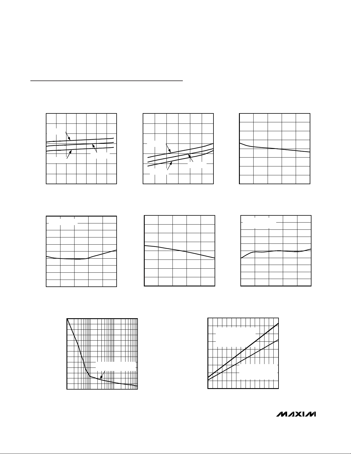
Typical Operating Characteristics
(V
IN1
= +6.5V to +13.2V, V
IN2
= +10V, V
IN3–IN6
= +2.7V to +5.5V, AUXIN_ = GPI_ = GND, MARGIN = MR = DBP, TA= +25°C,
unless otherwise noted.)
SUPPLY CURRENT
vs. SUPPLY VOLTAGE (IN1)
MAX6870/71 toc01
SUPPLY VOLTAGE (V)
SUPPLY CURRENT (mA)
12.511.510.59.58.57.5
0.9
1.0
1.1
1.2
1.3
1.4
1.5
0.8
6.5 13.5
TA = +85°C
TA = +25°C
TA = -40°C
SUPPLY CURRENT
vs. SUPPLY VOLTAGE (IN3 TO IN6)
MAX6870/71 toc02
SUPPLY VOLTAGE (V)
SUPPLY CURRENT (mA)
5.04.54.03.53.0
0.9
1.0
1.1
1.2
1.3
1.4
1.5
0.8
2.5 5.5
TA = +25°C
TA = +85°C
TA = -40°C
NORMALIZED PO_ TIMEOUT PERIOD
vs. TEMPERATURE
MAX6870/71 toc03
TEMPERATURE (°C)
NORMALIZED PO_ TIMEOUT PERIOD
6035-15 10
0.97
0.98
0.99
1.00
1.02
1.01
1.03
1.04
0.96
-40 85
IN_ TO PO_
PROPAGATION DELAY vs. TEMPERATURE
MAX6870/71 toc04
TEMPERATURE (°C)
IN_ TO PO_ OUTPUT PROPAGATION DELAY (µs)
603510-15
12
14
16
18
20
22
24
26
28
30
10
-40 85
100mV OVERDRIVE
NORMALIZED WATCHDOG TIMEOUT PERIOD
vs. TEMPERATURE
MAX6870/71 toc05
TEMPERATURE (°C)
NORMALIZED WATCHDOG TIMEOUT PERIOD
6035-15 10
0.985
0.990
0.995
1.000
1.010
1.005
1.015
1.020
0.980
-40 85
NORMALIZED IN_ THRESHOLD
vs. TEMPERATURE
MAX6870/71 toc06
TEMPERATURE (°C)
NORMALIZED IN_ THRESHOLD
603510-15
0.992
0.994
0.996
0.998
1.000
1.002
1.004
1.006
1.008
1.010
0.990
-40 85
IN3 THRESHOLD = 1V,
20mV/STEP RANGE
MAXIMUM IN_ TRANSIENT DURATION
vs. IN_ THRESHOLD OVERDRIVE
MAX6870/71 toc07
IN_ THRESHOLD OVERDRIVE (mV)
MAXIMUM_ TRANSIENT DURATION (µs)
10010
10
20
30
40
50
60
70
80
90
100
110
120
130
0
1 1000
PO_ ASSERTION
OCCURS ABOVE THIS LINE
OUTPUT VOLTAGE LOW
vs. SINK CURRENT
MAX6870/71 toc08
I
SINK
(mA)
V
OL
(mV)
131210
11
3456 789
1
2
50
100
150
200
250
300
350
400
450
0
014
15
OPEN-DRAIN, CHARGE
PUMP, OR WEAK PULLUP
PO1–PO4 (MAX6870)
PO1/PO2 (MAX6871)
PUSH-PULL
PO5–PO8 (MAX6870)
PO3/PO4/PO5 (MAX6871)
Page 7
MAX6870/MAX6871
EEPROM-Programmable Hex/Quad
Power-Supply Sequencers/Supervisors with ADC
_______________________________________________________________________________________ 7
OUTPUT VOLTAGE HIGH vs. SOURCE CURRENT
(PUSH-PULL OUTPUT)
MAX6870/71 toc10
I
OUT
(mA)
V
OH
(V)
555040 4510 15 20 25 30 355
0.5
1.0
1.5
2.0
2.5
3.0
3.5
4.0
4.5
5.0
5.5
6.0
0
060
PUSH-PULL TO IN3
IN3 = 5V
PO5–PO8 (MAX6870)
PO3/PO4/PO5 (MAX6871)
OUTPUT VOLTAGE HIGH vs. SOURCE CURRENT
(CHARGE-PUMP OUTPUT)
MAX6870/71 toc11
SOURCE CURRENT (µA)
OUTPUT VOLTAGE HIGH (V)
4321
3.5
4.0
4.5
5.0
5.5
6.0
3.0
05
MEASURED RELATIVE TO V
ABP
PO1–PO4 (MAX6870)
PO1/PO2 (MAX6871)
MR TO PO_ PROPAGATION DELAY
vs. TEMPERATURE
MAX6870/71 toc12
TEMPERATURE (°C)
MR TO PO_ PROPAGATION DELAY (µs)
6035-15 10
1.55
1.60
1.65
1.70
1.80
1.75
1.85
1.90
1.50
-40 85
MAXIMUM MR TRANSIENT DURATION
vs. MR THRESHOLD OVERDRIVE
MAX6870/71 toc13
MR THRESHOLD OVERDRIVE (mV)
MAXIMUM MR TRANSIENT DURATION (µs)
10010
0.1
0.2
0.3
0.4
0.5
0.6
0.7
0.8
0.9
1.0
1.1
1.2
0
1 1000
PO_ ASSERTION OCCURS
ABOVE THIS LINE
OUTPUT VOLTAGE HIGH vs. SOURCE CURRENT
(WEAK PULLUP OUTPUT)
MAX6870/71 toc09
I
OUT
(mA)
V
OH
(V)
4.54.03.0 3.51.0 1.5 2.0 2.50.5
0.5
1.0
1.5
2.0
2.5
3.0
3.5
4.0
4.5
5.0
5.5
6.0
0
05.0
WEAK PULLUP
TO ABP
Typical Operating Characteristics (continued)
(V
IN1
= +6.5V to +13.2V, V
IN2
= +10V, V
IN3–IN6
= +2.7V to +5.5V, AUXIN_ = GPI_ = GND, MARGIN = MR = DBP, TA= +25°C,
unless otherwise noted.)
ADC ACCURACY
vs. TEMPERATURE
MAX6870/71 toc14
TEMPERATURE (°C)
TOTAL UNADJUSTED ERROR (%)
603510-15
-0.8
-0.6
-0.4
-0.2
0
0.2
0.4
0.6
0.8
1.0
-1.0
-40 85
V
IN2
= -12V,
50mV/STEP RANGE
V
IN3
= 5V,
20mV/STEP RANGE
V
IN1
= 9V,
25mV/STEP RANGE
V
AUXIN1
= 1V
FET (IRF7811W)
TURN-ON WITH CHARGE PUMP
MAX6870/71 toc15
V
PO1
10V/div
V
SOURCE
2V/div
I
DRAIN
5A/div
SEE FIGURE 9
Page 8
MAX6870/MAX6871
EEPROM-Programmable Hex/Quad
Power-Supply Sequencers/Supervisors with ADC
8 _______________________________________________________________________________________
Pin Description
PIN
NAME
FUNCTION
1 3 PO2
Programmable Output 2. Configurable, active-high, active-low, open-drain, weak pullup, or
charge-pump output. PO2 pulls low with a 10µA internal current sink for +1V < V
ABP
< V
UVLO
.
PO2 assumes its programmed conditional output state when ABP exceeds UVLO.
2 5 PO3
Programmable Output 3. Configurable, active-high, active-low, open-drain, weak pullup
(MAX6870), push-pull (MAX6871), or charge-pump (MAX6870) output. PO3 pulls low with a
10µA internal current sink for +1V < V
ABP
< V
UVLO
. PO3 assumes its programmed conditional
output state when ABP exceeds UVLO.
3 6 PO4
Programmable Output 4. Configurable, active-high, active-low, open-drain, weak pullup
(MAX6870), push-pull (MAX6871), or charge-pump (MAX6870) output. PO4 pulls low with a
10µA internal current sink for +1V < V
ABP
< V
UVLO
. PO4 assumes its programmed conditional
output state when ABP exceeds UVLO.
4 4 GND Ground
5 7 PO5
Programmable Output 5. Configurable, active-high, active-low, open-drain, weak pullup, or
push-pull output. PO5 pulls low with a 10µA internal current sink for +1V < V
ABP
< V
UVLO
. PO5
assumes its programmed conditional output state when ABP exceeds UVLO.
6 — PO6
Programmable Output 6. Configurable, active-high, active-low, open-drain, weak pullup, or
push-pull output. PO6 pulls low with a 10µA internal current sink for +1V < V
ABP
< V
UVLO
. PO6
assumes its programmed conditional output state when ABP exceeds UVLO.
7 — PO7
Programmable Output 7. Configurable, active-high, active-low, open-drain, weak pullup, or
push-pull output. PO7 pulls low with a 10µA internal current sink for +1V < V
ABP
< V
UVLO
. PO7
assumes its programmed conditional output state when ABP exceeds UVLO.
8 — PO8
Programmable Output 8. Configurable, active-high, active-low, open-drain, weak pullup, or
push-pull output. PO8 pulls low with a 10µA internal current sink for +1V < V
ABP
< V
UVLO
.
PO8 assumes its programmed conditional output state when ABP exceeds UVLO.
9, 10
1, 8, 9, 10,
N.C. No Connection. Not internally connected.
11 11
Margin Input. Configure MARGIN to either assert PO_ into a programmed state or to hold PO_
in its existing state when driving MARGIN low. See Table 8. Leave MARGIN unconnected or
connect to DBP if unused. MARGIN overrides MR if both assert at the same time. MARGIN is
internally pulled up to DBP through a 10µA current source.
12 12 MR
Manual Reset Input. Configure MR to either assert PO_ into a programmed state or to have no
effect on PO_ when driving MR low. See Table 7. Leave MR unconnected or connect to DBP if
unused. MR is internally pulled up to DBP through a 10µA current source.
13 13 SDA Serial Data Input/Output (Open-Drain). SDA requires an external pullup resistor.
14 14 SCL Serial Clock Input. SCL requires an external pullup resistor.
15 15 A0
Address Input 0. Address inputs allow up to four MAX6870/MAX6871 connections on one
common bus. Connect A0 to GND or to the serial interface power supply.
16 16 A1
Address Input 1. Address inputs allow up to four MAX6870/MAX6871 connections on one
common bus. Connect A1 to GND or to the serial interface power supply.
MAX6870 MAX6871
25, 26, 32
MARGIN
Page 9
MAX6870/MAX6871
EEPROM-Programmable Hex/Quad
Power-Supply Sequencers/Supervisors with ADC
_______________________________________________________________________________________ 9
Pin Description (continued)
PIN
MAX6870
FUNCTION
17 17 GPI4
General-Purpose Logic Input 4. An internal 10µA current source pulls GPI4 to GND. Configure
GPI4 to control watchdog timer functions or the programmable outputs.
18 18 GPI3
General-Purpose Logic Input 3. An internal 10µA current source pulls GPI3 to GND. Configure
GPI3 to control watchdog timer functions or the programmable outputs.
19 19 GPI2
General-Purpose Logic Input 2. An internal 10µA current source pulls GPI2 to GND. Configure
GPI2 to control watchdog timer functions or the programmable outputs.
20 20 GPI1
General-Purpose Logic Input 1. An internal 10µA current source pulls GPI1 to GND. Configure
GPI1 to control watchdog timer functions or the programmable outputs.
21 21 ABP
Internal Power-Supply Output. Bypass ABP to GND with a 1µF ceramic capacitor. ABP powers
the internal circuitry of the MAX6870/MAX6871. ABP supplies the input voltage to the internal
charge pumps when the programmable outputs are configured as charge-pump outputs. Do
not use ABP to supply power to external circuitry.
22 22 DBP
Internal Digital Power-Supply Output. Bypass DBP to GND with a 1µF ceramic capacitor. DBP
supplies power to the EEPROM memory and the internal logic circuitry. Do not use DBP to
supply power to external circuitry.
23 23
Auxiliary Input 2. A 10-bit ADC monitors the input voltage at AUXIN2. The high-impedance
AUXIN2 input accepts input voltages up to V
REFIN
. AUXIN2 does not influence EEPROM-
configurable power-supply sequencing or reset detection functions.
24 24
Auxiliary Input 1. A 10-bit ADC monitors the input voltage at AUXIN1. The high-impedance
AUXIN1 input accepts input voltages up to V
REFIN
. AUXIN1 does not influence EEPROM-
configurable power-supply sequencing or reset detection functions.
25 — IN6
Voltage Input 6. Configure IN6 to detect voltage thresholds between +1V and +5.5V in 20mV
increments, or +0.5V to +3.05V in 10mV increments. For improved noise immunity, bypass IN6
to GND with a 0.1µF capacitor installed as close to the device as possible.
26 — IN5
Voltage Input 5. Configure IN5 to detect voltage thresholds between +1V and +5.5V in 20mV
increments, or +0.5V to +3.05V in 10mV increments. For improved noise immunity, bypass IN5
to GND with a 0.1µF capacitor installed as close to the device as possible.
27 27 IN4
Voltage Input 4. Configure IN4 to detect voltage thresholds between +1V and +5.5V in 20mV
increments, or +0.5V to +3.05V in 10mV increments. For improved noise immunity, bypass IN4
to GND with a 0.1µF capacitor installed as close to the device as possible.
28 28 IN3
Voltage Input 3. Configure IN3 to detect voltage thresholds between +1V and +5.5V in 20mV
increments, or +0.5V to +3.05V in 10mV increments. For improved noise immunity, bypass IN3
to GND with a 0.1µF capacitor installed as close to the device as possible.
29 29 IN2
Bipolar Voltage Input 2. Configure IN2 to detect negative voltage thresholds from -2.5V to
-15.25V in 50mV increments or -1.25V to -7.625V in 25mV increments. Alternatively, configure
IN2 to detect positive voltage thresholds from +2.5V to +15.25V in 50mV increments or +1.25V
to +7.625V in 25mV increments. For improved noise immunity, bypass IN2 to GND with a 0.1µF
capacitor installed as close to the device as possible.
MAX6871
NAME
AUXIN2
AUXIN1
Page 10
MAX6870/MAX6871
Detailed Description
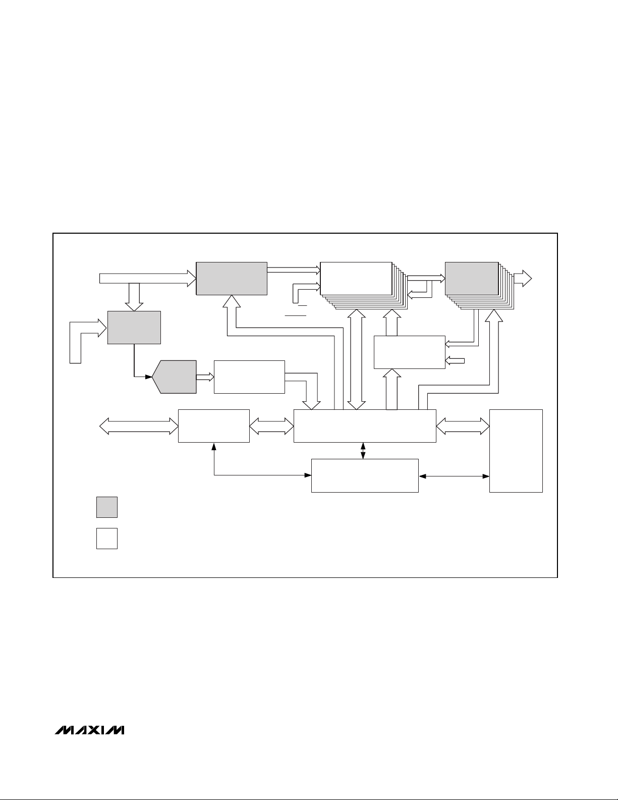
The MAX6870/MAX6871 EEPROM-configurable, multivoltage supply sequencers/supervisors monitor several
voltage-detector inputs, two auxiliary inputs and four
general-purpose logic inputs, and feature programmable outputs for highly-configurable, power-supply
sequencing applications. The MAX6870 features six
voltage-detector inputs and eight programmable outputs, while the MAX6871 features four voltage-detector
inputs and five programmable outputs. Manual reset
and margin disable inputs simplify board-level testing
during the manufacturing process. The MAX6870/
MAX6871 feature an accurate internal 1.25V reference.
For greater accuracy, connect an external +1.25V reference to REFIN.
All voltage detectors provide two configurable thresholds for undervoltage/overvoltage or dual undervoltage
detection. One high-voltage input (IN1) provides detector threshold voltages from +1.25V to +7.625V in 25mV
increments or +2.5V to +13.2V in 50mV increments.
A bipolar input (IN2) provides detector threshold voltages from ±1.25V to ±7.625V in 25mV increments, or
±2.5V to ±15.25V in 50mV increments. Positive inputs
(IN3–IN6) provide detector threshold voltages from
+0.5V to +3.05V in 10mV increments, or +1.0V to +5.5V
in 20mV increments.
An internal 10-bit ADC monitors the voltage-detector
inputs and two auxiliary inputs through a multiplexer
that automatically sequences through all inputs every
200ms. The host controller communicates with the
MAX6870/MAX6871s’ internal 4kb user EEPROM,
configuration EEPROM, configuration registers, ADC
registers, and fault registers through an SMBus/I
2
C-
compatible serial interface (see Figure 1).
Programmable output options include active-high,
active-low, open-drain, weak pullup, push-pull, and
charge pump. Select the charge-pump output feature
to drive n-channel FETs for power-supply sequencing
(see the Applications Information section). The outputs
swing between 0 and (V
ABP
+ 5V) when configured for
charge-pump operation.
Program each output to assert on any voltage-detector
input, general-purpose logic input, watchdog timer,
manual reset, or other output stages. Programmable
timing-delay blocks configure each output to wait
between 25µs and 1600ms before deasserting. A fault
register logs the conditions that caused each output to
assert (undervoltage, overvoltage, manual reset, etc.).
The MAX6870/MAX6871 feature two watchdog timers,
adding flexibility. Program each watchdog timer to assert
one or more programmable outputs. Program each
EEPROM-Programmable Hex/Quad
Power-Supply Sequencers/Supervisors with ADC
10 ______________________________________________________________________________________
Pin Description (continued)
PIN
MAX6870
NAME
FUNCTION
30 30 IN1
High Voltage Input 1. Configure IN1 to detect voltage thresholds from +2.5V to +13.2V in 50mV
increments or +1.25V to +7.625V in 25mV increments. For improved noise immunity, bypass
IN1 to GND with a 0.1µF capacitor installed as close to the device as possible.
31 31
Reference Voltage Input. Configure the MAX6870/MAX6871 to use either an internal reference
or external reference (see Table 9). When configured for an internal reference, leave REFIN
unconnected. When configured for an external reference, connect a +1.225V to +1.275V
reference to REFIN.
32 2 PO1
Programmable Output 1. Configurable active-high, active-low, open-drain, weak pullup, or
charge-pump output. PO1 pulls low with a weak 10µA internal current sink for +1V < V
ABP
< V
UVLO
. PO1 assumes its programmed conditional output state when ABP exceeds UVLO.
——EP Exposed Paddle. Exposed paddle is internally connected to GND.
MAX6871
REFIN
Page 11
MAX6870/MAX6871
EEPROM-Programmable Hex/Quad
Power-Supply Sequencers/Supervisors with ADC
______________________________________________________________________________________ 11
COMPARATORS
ADC
MUX
ADC
ADC REGISTERS
REGISTER BANK
CONTROLLER
EEPROM
(USER AND
CONFIG)
OUTPUT
STAGES
LOGIC NETWORK
FOR PO_
WATCHDOG
TIMERS
GPI_
GPI_, MR,
MARGIN
PO_
IN_
SDA,
SCL
ANALOG
BLOCK
DIGITAL
BLOCK
SERIAL
INTERFACE
AUXIN_
Figure 1. Top Level Block Diagram
watchdog timer to clear on a combination of one GPI_
input and one programmable output, one of the GPI_
inputs only, or one of the programmable outputs only.
The initial and normal watchdog timeout periods are
independently programmable from 6.25ms to 102.4s.
A virtual diode-ORing scheme selects the input that powers the MAX6870/MAX6871. The MAX6870/MAX6871
derive power from IN1 if V
IN1
> +6.5V or from the highest
voltage on IN3–IN6 if V
IN1
< +2.7V. The power source
cannot be determined if +4V < V
IN1
< +6.5V and one
of V
IN3
through V
IN6
> +2.7V. The programmable outputs maintain the correct programmed logic state for
V
ABP
> V
UVLO
. One of IN3 through IN6 must be
greater than +2.7V or IN1 must be greater than +4V for
device operation.
Page 12
MAX6870/MAX6871
EEPROM-Programmable Hex/Quad
Power-Supply Sequencers/Supervisors with ADC
12 ______________________________________________________________________________________
ADC
TIMING
SERIAL
INTERFACE
MAX6870
MAX6871
1.25V
V
REF
IN2 DETECTOR
IN_ DETECTOR
IN1
IN2
IN3
IN4
AUXIN1
AUXIN2
IN5
(N.C.)
IN6
(N.C.)
IN3 DETECTOR
IN4 DETECTOR
IN5 DETECTOR
IN6 DETECTOR
PROGRAMMABLE
ARRAY
TIMING BLOCK 2
TIMING BLOCK 3
TIMING BLOCK 4
TIMING BLOCK 5
TIMING BLOCK 6
TIMING BLOCK 7
TIMING BLOCK 8
PO2 OUTPUT
PO3 OUTPUT
PO4 OUTPUT
PO5 OUTPUT
PO6 OUTPUT
PO7 OUTPUT
PO8 OUTPUT
ADC
REGISTERS
TIMING BLOCK 1
V
ABP
+ 5V
CHARGE PUMP*
MUX
GPI1
GPI2
GPI3
GPI4
MARGIN
MR
IN3–IN6
(IN3–IN4)
PO_
OUTPUT
*PO1–PO4 ONLY
(PO1, PO2)
ABP
MUX
P1**
10kΩ
PO1
PO2
PO3
PO4
PO5
PO6
(N.C.)
PO7
(N.C.)
PO8
(N.C.)
SDA
SCL
A0
A1
OPENDRAIN
** PO5–PO8 ONLY
(PO3, PO4, PO5)
ADC
MUX
MAIN
OSCILLATOR
IN1
IN2
IN3
IN4
IN5
IN6
AUXIN1
AUXIN2
EEPROM
CHARGE PUMP
CONFIG
REGISTERS
CONFIG
EEPROM
USER
EEPROM
1µF
ABP
DBP
1µF
2.55V
LDO
5.4V
LDO
(VIRTUAL
DIODES)
REFIN
GND
( ) ARE FOR MAX6871 ONLY.
ADC
Functional Diagram
Page 13

MAX6870/MAX6871
EEPROM-Programmable Hex/Quad
Power-Supply Sequencers/Supervisors with ADC
______________________________________________________________________________________ 13
Powering the MAX6870/MAX6871
The MAX6870/MAX6871 derive power from the positive
voltage-detector inputs: IN1, or IN3–IN6. A virtual diodeORing scheme selects the positive input that supplies
power to the device (see the Functional Diagram). IN1
must be at least +4V or one of IN3–IN6 (MAX6870)/
IN3/IN4 (MAX6871) must be at least +2.7V to ensure
device operation. An internal LDO regulates IN1 down
to +5.4V.
The highest input voltage on IN3–IN6 (MAX6870)/
IN3/IN4 (MAX6871) supplies power to the device, unless
V
IN1
≥ +6.5V, in which case IN1 supplies power to the
device. For +4V < V
IN1
< +6.5V and one of V
IN3
through
V
IN6
> +2.7V, the input power source cannot be determined due to the dropout voltage of the LDO. Internal
hysteresis ensures that the supply input that initially powered the device continues to power the device when
multiple input voltages are within 50mV of each other.
ABP powers the analog circuitry; bypass ABP to GND
with a 1µF ceramic capacitor installed as close to the
device as possible. The internal supply voltage, measured at ABP, equals the maximum of IN3–IN6
(MAX6870)/IN3/IN4 (MAX6871) if V
IN1
= 0, or equals
+5.4V when V
IN1
> +6.5V. Do not use ABP to provide
power to external circuitry.
The MAX6870/MAX6871 also generate a digital supply
voltage (DBP) for the internal logic circuitry and the
EEPROM; bypass DBP to GND with a 1µF ceramic
capacitor installed as close to the device as possible.
The nominal DBP output voltage is +2.55V. Do not use
DBP to provide power to external circuitry.
ADC
The MAX6870/MAX6871 feature an internal 10-bit ADC
that monitors the voltage-detector inputs and auxiliary
inputs through an internal multiplexer that sequences
through all input voltages in 200ms. Registers 50h to
5Fh store the ADC data. Read the ADC data from the
MAX6870/MAX6871 with the serial interface. The ADC
strictly monitors input voltages and has no effect on
power-supply sequencing, reset detection, or the programmable outputs.
Inputs
The MAX6870/MAX6871 contain multiple logic and voltage-detector inputs. Each voltage-detector input is
simultaneously monitored for primary and secondary
thresholds. The primary threshold must be an undervoltage threshold. The secondary threshold may be an
undervoltage or overvoltage threshold. Table 1 summarizes these various inputs.
Table 1. Programmable Features
FEATURE DESCRIPTION
High Voltage Input
(IN1)
• Primary undervoltage threshold
• Secondary overvoltage or undervoltage threshold
• +2.5V to +13.2V threshold in 50mV increments
• +1.25V to +7.625V threshold in 25mV increments
Bipolar Voltage Input
(IN2)
• Primary undervoltage threshold
• Secondary overvoltage or undervoltage threshold
• ±2.5V to ±15.25V threshold in 50mV increments
• ±1.25V to ±7.625V threshold in 25mV increments
Positive Voltage Input
IN3–IN6 (MAX6870)
IN3, IN4 (MAX6871)
• Primary undervoltage threshold
• Secondary overvoltage or undervoltage threshold
• +1V to +5.5V threshold in 20mV increments
• +0.5V to +3.05V threshold in 10mV increments
Programmable Outputs
PO1–PO4 (MAX6870),
PO1, PO2 (MAX6871)
• Active high or active low
• Open-drain, weak pullup, or charge-pump output
• Weak pullup to IN3–IN6 (IN3 or IN4 for MAX6871) or ABP
• Dependent on MR, MARGIN, IN_, GPI1–GPI4 , WDI1 and WDI2, and/or PO_
• Programmable timeout periods of 25µs, 1.5625ms, 6.25ms, 25ms, 50ms, 200ms, 400ms, or 1.6s
Programmable Outputs
PO5–PO8 (MAX6870),
PO3, PO4, PO5
(MAX6871)
• Active high or active low
• Open-drain, weak pullup, or push-pull output
• Weak pullup to IN3–IN6 (IN3 or IN4 for MAX6871) or ABP
• Push-pull to IN3–IN6 (IN3 or IN4 for MAX6871)
• Dependent on MR, MARGIN, IN_, GPI1–GPI4 , WDI1 and WDI2 , and/or IN_
• Programmable timeout periods of 25µs, 1.5625ms, 6.25ms, 25ms, 50ms, 200ms, 400ms, or 1.6s
Page 14

Set the primary and secondary threshold voltages for
each voltage-detector input with registers 00h–0Bh.
Each primary threshold voltage must be an undervoltage threshold. Configure each secondary threshold
voltage as an undervoltage or overvoltage threshold
(see register 0Ch). Set the threshold range for each
voltage detector with register 0Dh.
High Voltage Input (IN1)
IN1 offers threshold voltages of +2.5V to +13.2V in
50mV increments, or +1.25V to +7.625V in 25mV increments. Use the following equations to set the threshold
voltages for IN1:
where V
TH
is the desired threshold voltage and x is the
decimal code for the desired threshold (Table 2). For
the +2.5V to +13.2V range, x must equal 214 or less,
otherwise the threshold exceeds the maximum operating voltage of IN1.
Bipolar Voltage Input (IN2)
IN2 offers negative thresholds from -2.5V to -15.25V in
50mV increments, or from -1.25V to -7.625V in 25mV
increments. Alternatively, IN2 offers positive thresholds
from +2.5V to +15.25V in 50mV increments, or +1.25V
to +7.625V in 25mV increments. Use the following
equations to set the threshold voltages for IN2:
x
VV
V
for V to V range
TH
=++
− .
.
. .
125
0 025
1 25 7 625
x
VV
V
for V to V range
TH
=++
− .
.
. .
25
005
2 5 13 2
MAX6870/MAX6871
EEPROM-Programmable Hex/Quad
Power-Supply Sequencers/Supervisors with ADC
14 ______________________________________________________________________________________
Table 1. Programmable Features (continued)
FEATURE DESCRIPTION
General-Purpose Logic
Inputs (GPI1–GPI4)
• Active high or active low logic levels
• Configure GPI_ as inputs to watchdog timers or programmable output stages
Watchdog Timers
• Clear dependent on any combination of one GPI_ input and one programmable output, a GPI_ input
only, or a programmable output only
• Initial watchdog timeout period of 6.25ms, 25ms, 100ms, 400ms, 1.6s, 6.4s, 25.6s, or 102.4s
• Normal watchdog timeout period of 6.25ms, 25ms, 100ms, 400ms, 1.6s, 6.4s, 25.6s, or 102.4s
• Watchdog enable/disable
• Initial watchdog timeout period enable/disable
Auxiliary Inputs
(AUXIN1, AUXIN2)
• Monitored by the internal 10-bit ADC
Manual Reset Input
(MR)
• Forces PO_ into the active output state when MR = GND
• PO_ deassert after MR releases high and the PO_ timeout period expires
• PO_ cannot be a function of MR only
Margining Input
(MARGIN)
• Holds PO_ in existing state or asserts PO_ to a programmed output state, independent of changes in
monitored inputs or watchdog timers, when MARGIN = GND
• Overrides MR when both assert at the same time
Reference Input
(REFIN)
• Internal +1.25V reference voltage
• Goes high-impedance when internal reference selected
• External reference voltage input from +1.225V to +1.275V
• Sets ADC voltage range
10-Bit ADC*
• Monitors IN_, AUXIN1, and AUXIN2
• Completes conversion of all eight inputs in 200ms
• Reference voltage sets ADC range
• Read ADC data from SMBus/I
2
C interface
Write Disable • Locks user EEPROM based on PO_
Configuration Lock • Locks configuration EEPROM
*ADC does not control programmable outputs.
Page 15
where VTHis the desired threshold voltage and x is the
decimal code for the desired threshold (Table 3).
IN3–IN6
IN3–IN6 offer positive voltage detectors monitor voltages from +1V to +5.5V in 20mV increments, or +0.5V
to +3.05V in 10mV increments. Use the following equations to set the threshold voltages for IN_:
where VTHis the desired threshold voltage and x is the
decimal code for the desired threshold (Table 4). For
the +1V to +5.5V range, x must equal 225 or less, otherwise the threshold exceeds the maximum operating
voltage of IN3–IN6.
x
VV
V
for V to V range
TH
=++
− .
.
. .
05
001
05 305
x
VV
V
for V to V range
TH
=++
−
.
.
1
002
155
x
VV
V
for V to V range
TH
=++
− .
.
. .
125
0 025
1 25 7 625
x
VV
V
for V to V range
TH
=++
− .
.
. .
25
005
2 5 15 25
x
VV
V
for V to V range
TH
=
()
−−
−− .
.
. .
125
0 025
1 25 7 625
x
VV
V
for V to V range
TH
=
()
−
−−
−
.
.
. .
25
005
2 5 15 25
MAX6870/MAX6871
EEPROM-Programmable Hex/Quad
Power-Supply Sequencers/Supervisors with ADC
______________________________________________________________________________________ 15
Table 2. IN1 Threshold Settings
REGISTER
ADDRESS
EEPROM
MEMORY
BIT
DESCRIPTION
00h 8000h [7:0]
IN1 primary undervoltage detector threshold (V1A) (see equations in the High Voltage Input
(IN1) section).
06h 8006h [7:0]
IN1 secondary undervoltage/overvoltage detector threshold (V1B) (see equations in the
High Voltage Input (IN1) section).
0Ch 800Ch [0]
IN1 secondary overvoltage/undervoltage selection.
0 = overvoltage threshold. 1 = undervoltage threshold.
0Dh 800Dh [0]
IN 1 r ang e sel ecti on.
0 = 2.5V to 13.2V r ang e i n 50m V i ncr em ents. 1 = 1.25V to 7.625V r ang e i n 25m V i ncr em ents.
Table 3. IN2 Threshold Settings
REGISTER
ADDRESS
EEPROM
MEMORY
BIT
DESCRIPTION
01h 8001h [7:0]
IN2 primary undervoltage detector threshold (V2A) (see equations in the Bipolar Voltage
Input (IN2) section).
07h 8007h [7:0]
IN2 secondary undervoltage/overvoltage detector threshold (V2B) (see equations in the
Bipolar Voltage Input (IN2) section).
0Ch 800Ch [1]
IN2 secondary overvoltage/undervoltage selection.
0 = overvoltage threshold. 1 = undervoltage threshold.
0Dh 800Dh [7:6]
IN2 range selection.
00 = -2.5V to -15.25V range in 50mV increments.
01 = -1.25V to -7.625V range in 25mV increments.
10 = +2.5V to +15.25V range in 50mV increments.
11 = +1.25V to +7.625V range in 25mV increments.
ADDRESS
RANGE
ADDRESS
RANGE
Page 16
MAX6870/MAX6871
EEPROM-Programmable Hex/Quad
Power-Supply Sequencers/Supervisors with ADC
16 ______________________________________________________________________________________
Table 4. IN3–IN6 Threshold Settings
REGISTER
ADDRESS
EEPROM
MEMORY
BIT
DESCRIPTION
02h 8002h [7:0] IN3 primary undervoltage detector threshold (V3A) (see equations in the IN3–IN6 section).
03h 8003h [7:0] IN4 primary undervoltage detector threshold (V4A) (see equations in the IN3–IN6 section).
04h 8004h [7:0]
IN5 (MAX6870 only) primary undervoltage detector threshold (V5A)
(see equations in the IN3–IN6 section).
05h 8005h [7:0]
IN6 (MAX6870 only) primary undervoltage detector threshold (V6A)
(see equations in the IN3–IN6 section).
08h 8008h [7:0]
IN3 secondary undervoltage/overvoltage detector threshold (V3B)
(see equations in the IN3–IN6 section).
09h 8009h [7:0]
IN4 secondary undervoltage/overvoltage detector threshold (V4B)
(see equations in the IN3–IN6 section).
0Ah 800Ah [7:0]
IN5 (MAX6870 only) secondary undervoltage/overvoltage detector threshold (V5B)
(see equations in the IN3–IN6 section).
0Bh 800Bh [7:0]
IN6 (MAX6870 only) secondary undervoltage/overvoltage detector threshold (V6B)
(see equations in the IN3–IN6 section).
[2]
IN3 secondary overvoltage/undervoltage selection.
0 = overvoltage threshold. 1 = undervoltage threshold.
[3]
IN4 secondary overvoltage/undervoltage selection.
0 = overvoltage threshold. 1 = undervoltage threshold.
[4]
IN5 (MAX6870 only) secondary overvoltage/undervoltage selection.
0 = overvoltage threshold. 1 = undervoltage threshold.
[5]
IN6 (MAX6870 only) secondary overvoltage/undervoltage selection.
0 = overvoltage threshold. 1 = undervoltage threshold.
0Ch 800Ch
[7:6] Not used.
[1]
IN 3 r ang e sel ecti on.
0 = + 1V to + 5.5V r ang e i n 20m V i ncr em ents. 1 = + 0.5V to + 3.05V r ang e i n 10m V i ncr em ents.
[2]
IN 4 r ang e sel ecti on.
0 = + 1V to + 5.5V r ang e i n 20m V i ncr em ents. 1 = + 0.5V to + 3.05V r ang e i n 10m V i ncr em ents.
[3]
IN 5 ( M AX 6870 onl y) r ang e sel ecti on.
0 = + 1V to + 5.5V r ang e i n 20m V i ncr em ents. 1 = + 0.5V to + 3.05V r ang e i n 10m V i ncr em ents.
[4]
IN 6 ( M AX 6870 onl y) r ang e sel ecti on.
0 = + 1V to + 5.5V r ang e i n 20m V i ncr em ents. 1 = + 0.5V to + 3.05V r ang e i n 10m V i ncr em ents.
0Dh 800Dh
[5] Not used.
ADDRESS
RANGE
Page 17

AUXIN1 and AUXIN2
The AUXIN1 and AUXIN2 high-impedance analog inputs
are intended to monitor two additional system voltages
not required for power-supply sequencing or reset purposes. The internal 10-bit ADC monitors AUXIN1 and
AUXIN2 and stores the data in the ADC registers (Table
5). AUXIN1 and AUXIN2 do not assert any of the programmable outputs. The AUXIN1 and AUXIN2 inputs
accept power-supply voltages or other system voltages
scaled to the +1.25V ADC input voltage range.
GPI1–GPI4
The GPI1–GPI4 programmable logic inputs control
power-supply sequencing (programmable outputs),
reset/interrupt signaling, and watchdog functions (see
the Configuring the Watchdog Timers (Registers
3Ch–3Fh) section). Configure GPI1–GPI4 for active-low
or active-high logic (Table 6). GPI1–GPI4 internally pull
down to GND through a 10µA current sink.
MR
The manual reset (MR) input initiates a reset condition.
Register 40h determines the programmable outputs that
assert while MR is low (Table 7). All affected programmable outputs remain asserted (see the Programmable
Outputs section) for their PO_ timeout periods after MR
releases high. An internal 10µA current source pulls MR
to DBP. Leave MR unconnected or connect to DBP if
unused. A programmable output cannot depend solely
on MR.
MAX6870/MAX6871
EEPROM-Programmable Hex/Quad
Power-Supply Sequencers/Supervisors with ADC
______________________________________________________________________________________ 17
Table 5. ADC Registers for AUXIN1 and
AUXIN2 (Read Only)
REGISTER
ADDRESS
BIT
DESCRIPTION
5Ch [7:0]
AUXIN1 measured value, 8 MSBs.
[1:0] AUXIN1 measured value, 2 LSBs.
5Dh
[7:2] Not used.
5Eh [7:0]
AUXIN2 measured value, 8 MSBs.
[1:0] AUXIN2 measured value, 2 LSBs.
5Fh
[7:2] Not used.
Table 6. GPI1–GPI4 Active Logic States
REGISTER
ADDRESS
BIT
D ESC R IPT IO N
[0] G P I1. 0 = acti ve l ow . 1 = acti ve hi g h.
[1] G P I2. 0 = acti ve l ow . 1 = acti ve hi g h.
[2] G P I3. 0 = acti ve l ow . 1 = acti ve hi g h.
3Bh
[3] G P I4. 0 = acti ve l ow . 1 = acti ve hi g h.
Table 7. Programmable Output Behavior and MR
REGISTER
ADDRESS
EEPROM
MEMORY
BIT
DESCRIPTION
[0] PO1 (MAX6870 only). 0 = PO1 independent of MR. 1 = PO1 asserts when MR = low.
[1] PO2 (MAX6870 only). 0 = PO2 independent of MR. 1 = PO2 asserts when MR = low.
[2]
PO3 (MAX6870)/PO1 (MAX6871). 0 = PO3/PO1 independent of MR.
1 = PO3/PO1 asserts when MR = low.
[3]
PO4 (MAX6870)/PO2 (MAX6871). 0 = PO4/PO2 independent of MR.
1 = PO4/PO2 asserts when MR = low.
[4]
PO5 (MAX6870)/PO3 (MAX6871). 0 = PO5/PO3 independent of MR.
1 = PO5/PO3 asserts when MR = low.
[5]
PO6 (MAX6870)/PO4 (MAX6871). 0 = PO6/PO4 independent of MR.
1 = PO6/PO4 asserts when MR = low.
[6]
PO7 (MAX6870)/PO5 (MAX6871). 0 = PO7/PO5 independent of MR.
1 = PO7/PO5 asserts when MR = low.
40h 8040h
[7] PO8 (MAX6870 only). 0 = PO8 independent of MR. 1 = PO8 asserts when MR = low.
RANGE
RANGE
ADDRESS
RANGE
Page 18

MAX6870/MAX6871
MARGIN
MARGIN allows system-level testing while power supplies exceed the normal ranges. Registers 41h and 42h
determine whether the programmable outputs assert to
a predetermined state or hold the last state as MARGIN
is driven low (Table 8). Drive MARGIN low to set the
programmable outputs in a known state while system-
level testing occurs. Leave MARGIN unconnected or
connect to DBP if unused. An internal 10µA current
source pulls MARGIN to DBP. The internal ADC continually monitors IN_ while MARGIN is low. The state of
each programmable output does not change while
MARGIN = GND. MARGIN overrides MR if both assert at
the same time.
EEPROM-Programmable Hex/Quad
Power-Supply Sequencers/Supervisors with ADC
18 ______________________________________________________________________________________
Table 8. Programmable Output Behavior and MARGIN
REGISTER
ADDRESS
EEPROM
MEMORY
BIT
AFFECTED OUTPUT DESCRIPTION
[0]
PO1
(MAX6870 only)
0 = output held in existing state.
1 = output asserts high or low (see 42h[0]).
[1]
PO2
(MAX6870 only)
0 = output held in existing state.
1 = output asserts high or low (see 42h[1]).
[2]
PO3 (MAX6870)
PO1 (MAX6871)
0 = output held in existing state.
1 = output asserts high or low (see 42h[2]).
[3]
PO4 (MAX6870)
PO2 (MAX6871)
0 = output held in existing state.
1 = output asserts high or low (see 42h[3]).
[4]
PO5 (MAX6870)
PO3 (MAX6871)
0 = output held in existing state.
1 = output asserts high or low (see 42h[4]).
[5]
PO6 (MAX6870)
PO4 (MAX6871)
0 = output held in existing state.
1 = output asserts high or low (see 42h[5]).
[6]
PO7 (MAX6870)
PO5 (MAX6871)
0 = output held in existing state.
1 = output asserts high or low (see 42h[6]).
41h 8041h
[7]
PO8
(MAX6870 only)
0 = output held in existing state.
1 = output asserts high or low (see 42h[7]).
[0]
PO1
(MAX6870 only)
0 = output asserts low if 41h[0] = 1.
1 = output asserts high if 41h[0] = 1.
[1]
PO2
(MAX6870 only)
0 = output asserts low if 41h[1] = 1.
1 = output asserts high if 41h[1] = 1.
[2]
PO3 (MAX6870)
PO1 (MAX6871)
0 = output asserts low if 41h[2] = 1.
1 = output asserts high if 41h[2] = 1.
[3]
PO4 (MAX6870)
PO2 (MAX6871)
0 = output asserts low if 41h[3] = 1.
1 = output asserts high if 41h[3] = 1.
[4]
PO5 (MAX6870)
PO3 (MAX6871)
0 = output asserts low if 41h[4] = 1.
1 = output asserts high if 41h[4] = 1.
[5]
PO6 (MAX6870)
PO4 (MAX6871)
0 = output asserts low if 41h[5] = 1.
1 = output asserts high if 41h[5] = 1.
[6]
PO7 (MAX6870)
PO5 (MAX6871)
0 = output asserts low if 41h[6] = 1.
1 = output asserts high if 41h[6] = 1.
42h 8042h
[7]
PO8
(MAX6870 only)
0 = output asserts low if 41h[7] = 1.
1 = output asserts high if 41h[7] = 1.
ADDRESS
RANGE
Page 19

REFIN
The MAX6870/MAX6871 feature an internal +1.25V voltage reference. The voltage reference sets the threshold
of the voltage detectors and provides a reference voltage for the internal ADC. Program register 44h to use
the internal reference or an external reference (Table
9). Leave REFIN unconnected when using the internal
reference. REFIN accepts an external reference in the
+1.225V to +1.275V range.
Programmable Outputs
The MAX6870 features eight programmable outputs,
while the MAX6871 features five programmable outputs.
Selectable output-stage configurations include: active low
or active high, open drain, weak pullup, push-pull, or
charge pump. During power-up, the programmable outputs pull to GND with an internal 10µA current sink for 1V
< V
ABP
< V
UVLO
. The programmable outputs remain in
their active states until PO_ timeout period expires, and
all of the programmed conditions are met for each output.
Any output programmed to depend on no condition
always remains in its active state (Table 22). An activehigh configured output is considered asserted when that
output is logic-high. No output can depend solely on MR.
The positive voltage monitors generate fault signals
(logical 0) to the MAX6870/MAX6871’s logic array when
an input voltage is below the programmed undervoltage threshold, or when that voltage is above the overvoltage threshold. The negative voltage monitor (IN2)
generates a fault signal to the logic array when the
input voltage is less negative than the undervoltage
threshold, or when that voltage is more negative than
the overvoltage threshold.
Registers 0Eh through 3Ah and 40h configure each of
the programmable outputs. Programmable timing
blocks set the PO_ timeout period from 25µs to 1600ms
for each programmable output. See register 3Ah (Table
22) to set the active state (active-high or active-low) for
each programmable output and registers 11h, 15h,
1Ch, 23h, 2Ah, 31h, 35h, and 39h to select the output
stage types (Tables 23 and 24), and PO_ timeout periods (Table 25) for each output.
Control selected programmable outputs with a sum of
products (Tables 10–21). Each product allows a different set of conditions to assert each output. Outputs
PO3 (MAX6870)/PO1 (MAX6871) and PO6 (MAX6870)/
PO4 (MAX6871) allow two sets of different conditions to
assert each output. Outputs PO1 and PO2 (MAX6870
only), PO7 (MAX6870)/PO5 (MAX6871), and PO8
(MAX6870 only) allow only one set of conditions to
assert each output.
For example, Product 1 of the PO3 (MAX6870—Table
12) programmable output may depend on the IN1 primary undervoltage threshold, and the states of GPI1,
PO1, and PO2. Write a one to R16h[0], R17h[6], and
R18h[3:2] to configure Product 1 as indicated. IN1
must be above the primary undervoltage threshold
(Table 2), GPI1 must be inactive (Table 6), and PO1
(Tables 10 and 22) and PO2 (Tables 12 and 23) must
be in their deasserted states for Product 1 to be a logical 1. Product 1 is equivalent to the logic statement:
V1A • GPI1 • PO1 • PO2.
Product 2 of PO3 (MAX6870, Table 13) may depend on
an entirely different set of conditions, or the same conditions, depending on the system requirements. For
example, Product 2 may depend on the IN1 undervoltage threshold, and the states of GPI2 and WDI1. Write
ones to R19h[6, 0] and R1Ah[7] to configure Product 2
as indicated. IN1 must be above the primary undervoltage threshold (Table 2), GPI2 must be inactive (Table
6), and the WDI1 timer must not have expired (Tables
27 and 28) for Product 2 to be a logical 1. Product 2 is
equivalent to the logic statement: V1A • GPI2 • WDI1.
PO3 deasserts if either Product 1 or Product 2 is a logical 1. The logical statement: Product 1 + Product 2
determines the state of PO3.
MAX6870/MAX6871
EEPROM-Programmable Hex/Quad
Power-Supply Sequencers/Supervisors with ADC
______________________________________________________________________________________ 19
Table 9. Reference Register
REGISTER
ADDRESS
EEPROM
MEMORY
BIT
DESCRIPTION
[0]
0 = internal reference.
1 = external reference.
44h 8044h
[7:1] Not used.
ADDRESS
RANGE
Page 20

MAX6870/MAX6871
Table 10 only applies to PO1 of the MAX6870. Write a 0
to a bit to make the PO1 output independent of the
respective signal (IN1–IN6 primary or secondary
thresholds, WDI1 or WDI2, GPI1–GPI4, MR, or other
programmable outputs).
EEPROM-Programmable Hex/Quad
Power-Supply Sequencers/Supervisors with ADC
20 ______________________________________________________________________________________
Table 10. PO1 (MAX6870 Only) Output Dependency
REGISTER
ADDRESS
EEPROM
MEMORY
BIT OUTPUT ASSERTION CONDITIONS
[0] 1 = PO1 assertion depends on IN1 primary undervoltage threshold (Table 2).
[1] 1 = PO1 assertion depends on IN2 primary undervoltage threshold (Table 3).
[2] 1 = PO1 assertion depends on IN3 primary undervoltage threshold (Table 4).
[3] 1 = PO1 assertion depends on IN4 primary undervoltage threshold (Table 4).
[4] 1 = PO1 assertion depends on IN5 primary undervoltage threshold (Table 4).
[5] 1 = PO1 assertion depends on IN6 primary undervoltage threshold (Table 4).
[6] 1 = PO1 assertion depends on watchdog 1 (Tables 27 and 28).
0Eh 800Eh
[7] 1 = PO1 assertion depends on watchdog 2 (Tables 27 and 28).
[0] 1 = P O1 asser ti on d ep end s on IN 1 second ar y und er vol tag e/over vol tag e thr eshol d ( Tab l e 2) .
[1] 1 = P O1 asser ti on d ep end s on IN 2 second ar y und er vol tag e/over vol tag e thr eshol d ( Tab l e 3) .
[2] 1 = P O1 asser ti on d ep end s on IN 3 second ar y und er vol tag e/over vol tag e thr eshol d ( Tab l e 4) .
[3] 1 = P O1 asser ti on d ep end s on IN 4 second ar y und er vol tag e/over vol tag e thr eshol d ( Tab l e 4) .
[4] 1 = P O1 asser ti on d ep end s on IN 5 second ar y und er vol tag e/over vol tag e thr eshol d ( Tab l e 4) .
[5] 1 = P O1 asser ti on d ep end s on IN 6 second ar y und er vol tag e/over vol tag e thr eshol d ( Tab l e 4) .
[6] 1 = PO1 assertion depends on GPI1 (Table 6).
0Fh 800Fh
[7] 1 = PO1 assertion depends on GPI2 (Table 6).
[0] 1 = PO1 assertion depends on GPI3 (Table 6).
[1] 1 = PO1 assertion depends on GPI4 (Table 6).
[2] 1 = PO1 assertion depends on PO2 (Table 11).
[3] 1 = PO1 assertion depends on PO3 (Tables 12 and 13).
[4] 1 = PO1 assertion depends on PO4 (Tables 14 and 15).
[5] 1 = PO1 assertion depends on PO5 (Tables 16 and 17).
[6] 1 = PO1 assertion depends on PO6 (Tables 18 and 19).
10h 8010h
[7] 1 = PO1 assertion depends on PO7 (Table 20).
11h 8011h [0] 1 = PO1 assertion depends on PO8 (Table 21).
40h 8040h [0] 1 = PO1 asserts when MR = low (Table 7).
ADDRESS
Page 21

Table 11 only applies to PO2 of the MAX6870. Write a 0
to a bit to make the PO2 output independent of the
respective signal (IN1–IN6 primary or secondary
thresholds, WDI1 or WDI2, GPI1–GPI4, MR, or other
programmable outputs).
MAX6870/MAX6871
EEPROM-Programmable Hex/Quad
Power-Supply Sequencers/Supervisors with ADC
______________________________________________________________________________________ 21
Table 11. PO2 (MAX6870 Only) Output Dependency
REGISTER
ADDRESS
EEPROM
MEMORY
BIT OUTPUT ASSERTION CONDITIONS
[0] 1 = PO2 assertion depends on IN1 primary undervoltage threshold (Table 2).
[1] 1 = PO2 assertion depends on IN2 primary undervoltage threshold (Table 3).
[2] 1 = PO2 assertion depends on IN3 primary undervoltage threshold (Table 4).
[3] 1 = PO2 assertion depends on IN4 primary undervoltage threshold (Table 4).
[4] 1 = PO2 assertion depends on IN5 primary undervoltage threshold (Table 4).
[5] 1 = PO2 assertion depends on IN6 primary undervoltage threshold (Table 4).
[6] 1 = PO2 assertion depends on watchdog 1 (Tables 27 and 28).
12h 8012h
[7] 1 = PO2 assertion depends on watchdog 2 (Tables 27 and 28).
[0] 1 = P O2 asser ti on d ep end s on IN 1 second ar y und er vol tag e/over vol tag e thr eshol d ( Tab l e 2) .
[1] 1 = P O2 asser ti on d ep end s on IN 2 second ar y und er vol tag e/over vol tag e thr eshol d ( Tab l e 3) .
[2] 1 = P O2 asser ti on d ep end s on IN 3 second ar y und er vol tag e/over vol tag e thr eshol d ( Tab l e 4) .
[3] 1 = P O2 asser ti on d ep end s on IN 4 second ar y und er vol tag e/over vol tag e thr eshol d ( Tab l e 4) .
[4] 1 = P O2 asser ti on d ep end s on IN 5 second ar y und er vol tag e/over vol tag e thr eshol d ( Tab l e 4) .
[5] 1 = P O2 asser ti on d ep end s on IN 6 second ar y und er vol tag e/over vol tag e thr eshol d ( Tab l e 4) .
[6] 1 = PO2 assertion depends on GPI1 (Table 6).
13h 8013h
[7] 1 = PO2 assertion depends on GPI2 (Table 6).
[0] 1 = PO2 assertion depends on GPI3 (Table 6).
[1] 1 = PO2 assertion depends on GPI4 (Table 6).
[2] 1 = PO2 assertion depends on PO1 (Table 10).
[3] 1 = PO2 assertion depends on PO3 (Tables 12 and 13).
[4] 1 = PO2 assertion depends on PO4 (Tables 14 and 15).
[5] 1 = PO2 assertion depends on PO5 (Tables 16 and 17).
[6] 1 = PO2 assertion depends on PO6 (Tables 18 and 19).
14h 8014h
[7] 1 = PO2 assertion depends on PO7 (Table 20).
15h 8015h [0] 1 = PO2 assertion depends on PO8 (Table 21).
40h 8040h [1] 1 = PO2 asserts when MR = low (Table 7).
ADDRESS
Page 22

MAX6870/MAX6871
Table 12 only applies to PO3 of the MAX6870 and PO1
of the MAX6871. Write a 0 to a bit to make the PO3/PO1
output independent of the respective signal (IN_ primary
or secondary thresholds, WDI1 or WDI2, GPI1–GPI4,
MR, or other programmable outputs). See Table 13 for
Product 2. PO3 (MAX6870)/PO1 (MAX6871) deasserts
when Product 1 or Product 2 = 1.
EEPROM-Programmable Hex/Quad
Power-Supply Sequencers/Supervisors with ADC
22 ______________________________________________________________________________________
Table 12. PO3 (MAX6870)/PO1 (MAX6871) Output Dependency (Product 1)
REGISTER
ADDRESS
EEPROM
MEMORY
BIT OUTPUT ASSERTION CONDITIONS
[0] 1 = PO3/PO1 assertion depends on IN1 primary undervoltage threshold (Table 2).
[1] 1 = PO3/PO1 assertion depends on IN2 primary undervoltage threshold (Table 3).
[2] 1 = PO3/PO1 assertion depends on IN3 primary undervoltage threshold (Table 4).
[3] 1 = PO3/PO1 assertion depends on IN4 primary undervoltage threshold (Table 4).
[4]
1 = PO3 (MAX6870 only) assertion depends on IN5 primary undervoltage threshold (Table 4).
Must be set to 0 for the MAX6871.
[5]
1 = PO3 (MAX6870 only) assertion depends on IN6 primary undervoltage threshold (Table 4).
Must be set to 0 for the MAX6871.
[6] 1 = PO3/PO1 assertion depends on watchdog 1 (Tables 27 and 28).
16h 8016h
[7] 1 = PO3/PO1 assertion depends on watchdog 2 (Tables 27 and 28).
[0] 1 = P O3/P O1 asser ti on d ep end s on IN 1 second ar y und er vol tag e/over vol tag e thr eshol d ( Tab l e 2) .
[1] 1 = P O3/P O1 asser ti on d ep end s on IN 2 second ar y und er vol tag e/over vol tag e thr eshol d ( Tab l e 3) .
[2] 1 = P O3/P O1 asser ti on d ep end s on IN 3 second ar y und er vol tag e/over vol tag e thr eshol d ( Tab l e 4) .
[3] 1 = P O3/P O1 asser ti on d ep end s on IN 4 second ar y und er vol tag e/over vol tag e thr eshol d ( Tab l e 4) .
[4]
1 = PO3 (MAX6870 only) assertion depends on IN5 secondary undervoltage/overvoltage
threshold (Table 4). Must be set to 0 for the MAX6871.
[5]
1 = PO3 (MAX6870 only) assertion depends on IN6 secondary undervoltage/overvoltage
threshold (Table 4). Must be set to 0 for the MAX6871.
[6] 1 = PO3/PO1 assertion depends on GPI1 (Table 6).
17h 8017h
[7] 1 = PO3/PO1 assertion depends on GPI2 (Table 6).
[0] 1 = PO3/PO1 assertion depends on GPI3 (Table 6).
[1] 1 = PO3/PO1 assertion depends on GPI4 (Table 6).
[2] 1 = P O3 ( M AX 6870 onl y) asser ti on d ep end s on P O1 ( Tab l e 10) . M ust b e set to 0 for the M AX 6871.
[3] 1 = P O3 ( M AX 6870 onl y) asser ti on d ep end s on P O2 ( Tab l e 11) . M ust b e set to 0 for the M AX 6871.
[4] 1 = PO3/PO1 assertion depends on PO4 (MAX6870)/PO2 (MAX6871) (Tables 14 and 15).
[5] 1 = P O3/P O 1 asser ti on d ep end s on P O5 ( M AX 6870) /P O 3 ( M AX 6871) ( Tab l es 16 and 17) .
[6] 1 = PO3/PO1 assertion depends on PO6 (MAX6870)/PO4 (MAX6871) (Tables 18 and 19).
18h 8018h
[7] 1 = PO3/PO1 assertion depends on PO7 (MAX6870)/PO5 (MAX6871) (Table 20).
1Ch 801Ch [0] 1 = P O3 ( M AX 6870 onl y) asser ti on d ep end s on P O8 ( Tab l e 21) . M ust b e set to 0 for the M AX 6871.
40h 8040h [2] 1 = PO3/PO1 asserts when MR = low (Table 7).
ADDRESS
Page 23

Table 13 only applies to PO3 of the MAX6870 and PO1
of the MAX6871. Write a 0 to a bit to make the PO3/PO1
output independent of the respective signal (IN_ primary
or secondary thresholds, WDI1 or WDI2, GPI1–GPI4,
MR, or other programmable outputs). See Table 12 for
Product 1. PO3 (MAX6870)/PO1 (MAX6871) deasserts
when Product 1 or Product 2 = 1.
MAX6870/MAX6871
EEPROM-Programmable Hex/Quad
Power-Supply Sequencers/Supervisors with ADC
______________________________________________________________________________________ 23
Table 13. PO3 (MAX6870)/PO1 (MAX6871) Output Dependency (Product 2)
REGISTER
ADDRESS
EEPROM
MEMORY
BIT OUTPUT ASSERTION CONDITIONS
[0] 1 = PO3/PO1 assertion depends on IN1 primary undervoltage threshold (Table 2).
[1] 1 = PO3/PO1 assertion depends on IN2 primary undervoltage threshold (Table 3).
[2] 1 = PO3/PO1 assertion depends on IN3 primary undervoltage threshold (Table 4).
[3] 1 = PO3/PO1 assertion depends on IN4 primary undervoltage threshold (Table 4).
[4]
1 = PO3 (MAX6870 only) assertion depends on IN5 primary undervoltage threshold (Table 4).
Must be set to 0 for the MAX6871.
[5]
1 = PO3 (MAX6870 only) assertion depends on IN6 primary undervoltage threshold (Table 4).
Must be set to 0 for the MAX6871.
[6] 1 = PO3/PO1 assertion depends on watchdog 1 (Tables 27 and 28).
19h 8019h
[7] 1 = PO3/PO1 assertion depends on watchdog 2 (Tables 27 and 28).
[0] 1 = P O3/P O1 asser ti on d ep end s on IN 1 second ar y und er vol tag e/over vol tag e thr eshol d ( Tab l e 2) .
[1] 1 = P O3/P O1 asser ti on d ep end s on IN 2 second ar y und er vol tag e/over vol tag e thr eshol d ( Tab l e 3) .
[2] 1 = P O3/P O1 asser ti on d ep end s on IN 3 second ar y und er vol tag e/over vol tag e thr eshol d ( Tab l e 4) .
[3] 1 = P O3/P O1 asser ti on d ep end s on IN 4 second ar y und er vol tag e/over vol tag e thr eshol d ( Tab l e 4) .
[4]
1 = PO3 (MAX6870 only) assertion depends on IN5 secondary undervoltage/overvoltage
threshold (Table 4). Must be set to 0 for the MAX6871.
[5]
1 = PO3 (MAX6870 only) assertion depends on IN6 secondary undervoltage/overvoltage
threshold (Table 4). Must be set to 0 for the MAX6871.
[6] 1 = PO3/PO1 assertion depends on GPI1 (Table 6).
1Ah 801Ah
[7] 1 = PO3/PO1 assertion depends on GPI2 (Table 6).
[0] 1 = PO3/PO1 assertion depends on GPI3 (Table 6).
[1] 1 = PO3/PO1 assertion depends on GPI4 (Table 6).
[2] 1 = P O3 ( M AX 6870 onl y) asser ti on d ep end s on P O1 ( Tab l e 10) . M ust b e set to 0 for the M AX 6871.
[3] 1 = P O3 ( M AX 6870 onl y) asser ti on d ep end s on P O2 ( Tab l e 11) . M ust b e set to 0 for the M AX 6871.
[4] 1 = P O3/P O 1 asser ti on d ep end s on P O4 ( M AX 6870) /P O 2 ( M AX 6871) ( Tab l es 14 and 15) .
[5] 1 = P O3/P O 1 asser ti on d ep end s on P O5 ( M AX 6870) /P O 3 ( M AX 6871) ( Tab l es 16 and 17) .
[6] 1 = P O3/P O 1 asser ti on d ep end s on P O6 ( M AX 6870) /P O 4 ( M AX 6871) ( Tab l es 18 and 19) .
1Bh 801Bh
[7] 1 = PO3/PO1 assertion depends on PO7 (MAX6870)/PO5 (MAX6871) (Table 20).
1Ch 801Ch [1] 1 = P O3 ( M AX 6870 onl y) asser ti on d ep end s on P O8 ( Tab l e 21) . M ust b e set to 0 for the M AX 6871.
40h 8040h [2] 1 = PO3/PO1 asserts when MR = low (Table 7).
ADDRESS
Page 24

MAX6870/MAX6871
Table 14 only applies to PO4 of the MAX6870 and PO2
of the MAX6871. Write a 0 to a bit to make the PO4/PO2
output independent of the respective signal (IN_ primary
or secondary thresholds, WDI1 or WDI2, GPI1–GPI4,
MR, or other programmable outputs). See Table 15 for
Product 2. PO4 (MAX6870)/PO2 (MAX6871) deasserts
when Product 1 or Product 2 = 1.
EEPROM-Programmable Hex/Quad
Power-Supply Sequencers/Supervisors with ADC
24 ______________________________________________________________________________________
Table 14. PO4 (MAX6870)/PO2 (MAX6871) Output Dependency (Product 1)
REGISTER
ADDRESS
EEPROM
MEMORY
BIT OUTPUT ASSERTION CONDITIONS
[0] 1 = PO4/PO2 assertion depends on IN1 primary undervoltage threshold (Table 2).
[1] 1 = PO4/PO2 assertion depends on IN2 primary undervoltage threshold (Table 3).
[2] 1 = PO4/PO2 assertion depends on IN3 primary undervoltage threshold (Table 4).
[3] 1 = PO4/PO2 assertion depends on IN4 primary undervoltage threshold (Table 4).
[4]
1 = P O4 ( M AX 6870 onl y) asser ti on d ep end s on IN 5 p r i m ar y und er vol tag e thr eshol d ( Tab l e 4) .
M ust b e set to 0 for the M AX 6871.
[5]
1 = P O4 ( M AX 6870 onl y) asser ti on d ep end s on IN 6 p r i m ar y und er vol tag e thr eshol d ( Tab l e 4) .
M ust b e set to 0 for the M AX 6871.
[6] 1 = PO4/PO2 assertion depends on watchdog 1 (Tables 27 and 28).
1Dh 801Dh
[7] 1 = PO4/PO2 assertion depends on watchdog 2 (Tables 27 and 28).
[0] 1 = P O4/P O2 asser ti on d ep end s on IN 1 second ar y und er vol tag e/over vol tag e thr eshol d ( Tab l e 2) .
[1] 1 = P O4/P O2 asser ti on d ep end s on IN 2 second ar y und er vol tag e/over vol tag e thr eshol d ( Tab l e 3) .
[2] 1 = P O4/P O2 asser ti on d ep end s on IN 3 second ar y und er vol tag e/over vol tag e thr eshol d ( Tab l e 4) .
[3] 1 = P O4/P O2 asser ti on d ep end s on IN 4 second ar y und er vol tag e/over vol tag e thr eshol d ( Tab l e 4) .
[4]
1 = PO4 (MAX6870 only) assertion depends on IN5 secondary undervoltage/overvoltage
threshold (Table 4). Must be set to 0 for the MAX6871.
[5]
1 = PO4 (MAX6870 only) assertion depends on IN6 secondary undervoltage/overvoltage
threshold (Table 4). Must be set to 0 for the MAX6871.
[6] 1 = PO4/PO2 assertion depends on GPI1 (Table 6).
1Eh 801Eh
[7] 1 = PO4/PO2 assertion depends on GPI2 (Table 6).
[0] 1 = PO4/PO2 assertion depends on GPI3 (Table 6).
[1] 1 = PO4/PO2 assertion depends on GPI4 (Table 6).
[2] 1 = P O4 ( M AX 6870 onl y) asser ti on d ep end s on P O1 ( Tab l e 10) . M ust b e set to 0 for the M AX 6871.
[3] 1 = P O4 ( M AX 6870 onl y) asser ti on d ep end s on P O2 ( Tab l e 11) . M ust b e set to 0 for the M AX 6871.
[4] 1 = P O4/P O 2 asser ti on d ep end s on P O3 ( M AX 6870) /P O 1 ( M AX 6871) ( Tab l es 12 and 13) .
[5] 1 = P O4/P O 2 asser ti on d ep end s on P O5 ( M AX 6870) /P O 3 ( M AX 6871) ( Tab l es 16 and 17) .
[6] 1 = P O4/P O 2 asser ti on d ep end s on P O6 ( M AX 6870) /P O 4 ( M AX 6871) ( Tab l es 18 and 19) .
1Fh 801Fh
[7] 1 = PO4/PO2 assertion depends on PO7 (MAX6870)/PO5 (MAX6871) (Table 20).
23h 8023h [0] 1 = P O4 ( M AX 6870 onl y) asser ti on d ep end s on P O8 ( Tab l e 21) . M ust b e set to 0 for the M AX 6871.
40h 8040h [3] 1 = PO4/PO2 asserts when MR = low (Table 7).
ADDRESS
Page 25

Table 15 only applies to PO4 of the MAX6870 and PO2
of the MAX6871. Write a 0 to a bit to make the PO4/PO2
output independent of the respective signal (IN_ primary
or secondary thresholds, WDI1 or WDI2, GPI1 to GPI4,
MR, or other programmable outputs). See Table 14 for
Product 1. PO4 (MAX6870)/PO2 (MAX6871) deasserts
when Product 1 or Product 2 = 1.
MAX6870/MAX6871
EEPROM-Programmable Hex/Quad
Power-Supply Sequencers/Supervisors with ADC
______________________________________________________________________________________ 25
Table 15. PO4 (MAX6870)/PO2 (MAX6871) Output Dependency (Product 2)
REGISTER
ADDRESS
EEPROM
MEMORY
BIT OUTPUT ASSERTION CONDITIONS
[0] 1 = PO4/PO2 assertion depends on IN1 primary undervoltage threshold (Table 2).
[1] 1 = PO4/PO2 assertion depends on IN2 primary undervoltage threshold (Table 3).
[2] 1 = PO4/PO2 assertion depends on IN3 primary undervoltage threshold (Table 4).
[3] 1 = PO4/PO2 assertion depends on IN4 primary undervoltage threshold (Table 4).
[4]
1 = PO4 (MAX6870 only) assertion depends on IN5 primary undervoltage threshold (Table 4).
Must be set to 0 for the MAX6871.
[5]
1 = PO4 (MAX6870 only) assertion depends on IN6 primary undervoltage threshold (Table 4).
Must be set to 0 for the MAX6871.
[6] 1 = PO4/PO2 assertion depends on watchdog 1 (Tables 27 and 28).
20h 8020h
[7] 1 = PO4/PO2 assertion depends on watchdog 2 (Tables 27 and 28).
[0] 1 = P O4/P O2 asser ti on d ep end s on IN 1 second ar y und er vol tag e/over vol tag e thr eshol d ( Tab l e 2) .
[1] 1 = P O4/P O2 asser ti on d ep end s on IN 2 second ar y und er vol tag e/over vol tag e thr eshol d ( Tab l e 3) .
[2] 1 = P O4/P O2 asser ti on d ep end s on IN 3 second ar y und er vol tag e/over vol tag e thr eshol d ( Tab l e 4) .
[3] 1 = P O4/P O2 asser ti on d ep end s on IN 4 second ar y und er vol tag e/over vol tag e thr eshol d ( Tab l e 4) .
[4]
1 = PO4 (MAX6870 only) assertion depends on IN5 secondary undervoltage/overvoltage
threshold (Table 4). Must be set to 0 for the MAX6871.
[5]
1 = PO4 (MAX6870 only) assertion depends on IN6 secondary undervoltage/overvoltage
threshold (Table 4). Must be set to 0 for the MAX6871.
[6] 1 = PO4/PO2 assertion depends on GPI1 (Table 6).
21h 8021h
[7] 1 = PO4/PO2 assertion depends on GPI2 (Table 6).
[0] 1 = PO4/PO2 assertion depends on GPI3 (Table 6).
[1] 1 = PO4/PO2 assertion depends on GPI4 (Table 6).
[2] 1 = P O4 ( M AX 6870 onl y) asser ti on d ep end s on P O1 ( Tab l e 10) . M ust b e set to 0 for the M AX 6871.
[3] 1 = P O4 ( M AX 6870 onl y) asser ti on d ep end s on P O2 ( Tab l e 11) . M ust b e set to 0 for the M AX 6871.
[4] 1 = PO4/PO2 assertion depends on PO3 (MAX6870)/PO1 (MAX6871) (Tables 12 and 13).
[5] 1 = PO4/PO2 assertion depends on PO5 (MAX6870)/PO3 (MAX6871) (Tables 16 and 17).
[6] 1 = PO4/PO2 assertion depends on PO6 (MAX6870)/PO4 (MAX6871) (Tables 18 and 19).
22h 8022h
[7] 1 = PO4/PO2 assertion depends on PO7 (MAX6870)/PO5 (MAX6871) (Table 20).
23h 8023h [1] 1 = P O4 ( M AX 6870 onl y) asser ti on d ep end s on P O8 ( Tab l e 21) . M ust b e set to 0 for the M AX 6871.
40h 8040h [3] 1 = PO4/PO2 asserts when MR = low (Table 7).
ADDRESS
Page 26

MAX6870/MAX6871
Table 16 only applies to PO5 of the MAX6870 and PO3
of the MAX6871. Write a 0 to a bit to make the PO5/PO3
output independent of the respective signal (IN_ primary
or secondary thresholds, WDI1 or WDI2, GPI1–GPI4,
MR, or other programmable outputs). See Table 17 for
Product 2. PO5 (MAX6870)/PO3 (MAX6871) deasserts
when Product 1 or Product 2 = 1.
EEPROM-Programmable Hex/Quad
Power-Supply Sequencers/Supervisors with ADC
26 ______________________________________________________________________________________
Table 16. PO5 (MAX6870)/PO3 (MAX6871) Output Dependency (Product 1)
REGISTER
ADDRESS
EEPROM
MEMORY
BIT OUTPUT ASSERTION CONDITIONS
[0] 1 = PO5/PO3 assertion depends on IN1 primary undervoltage threshold (Table 2).
[1] 1 = PO5/PO3 assertion depends on IN2 primary undervoltage threshold (Table 3).
[2] 1 = PO5/PO3 assertion depends on IN3 primary undervoltage threshold (Table 4).
[3] 1 = PO5/PO3 assertion depends on IN4 primary undervoltage threshold (Table 4).
[4]
1 = PO5 (MAX6870 only) assertion depends on IN5 primary undervoltage threshold (Table 4).
Must be set to 0 for the MAX6871.
[5]
1 = PO5 (MAX6870 only) assertion depends on IN6 primary undervoltage threshold (Table 4).
Must be set to 0 for the MAX6871.
[6] 1 = PO5/PO3 assertion depends on watchdog 1 (Tables 27 and 28).
24h 8024h
[7] 1 = PO5/PO3 assertion depends on watchdog 2 (Tables 27 and 28).
[0] 1 = P O5/P O3 asser ti on d ep end s on IN 1 second ar y und er vol tag e/over vol tag e thr eshol d ( Tab l e 2) .
[1] 1 = P O5/P O3 asser ti on d ep end s on IN 2 second ar y und er vol tag e/over vol tag e thr eshol d ( Tab l e 3) .
[2] 1 = P O5/P O3 asser ti on d ep end s on IN 3 second ar y und er vol tag e/over vol tag e thr eshol d ( Tab l e 4) .
[3] 1 = P O5/P O3 asser ti on d ep end s on IN 4 second ar y und er vol tag e/over vol tag e thr eshol d ( Tab l e 4) .
[4]
1 = PO5 (MAX6870 only) assertion depends on IN5 secondary undervoltage/overvoltage
threshold (Table 4). Must be set to 0 for the MAX6871.
[5]
1 = PO5 (MAX6870 only) assertion depends on IN6 secondary undervoltage/overvoltage
threshold (Table 4). Must be set to 0 for the MAX6871.
[6] 1 = PO5/PO3 assertion depends on GPI1 (Table 6).
25h 8025h
[7] 1 = PO5/PO3 assertion depends on GPI2 (Table 6).
[0] 1 = PO5/PO3 assertion depends on GPI3 (Table 6).
[1] 1 = PO5/PO3 assertion depends on GPI4 (Table 6).
[2] 1 = P O5 ( M AX 6870 onl y) asser ti on d ep end s on P O1 ( Tab l e 10) . M ust b e set to 0 for the M AX 6871.
[3] 1 = P O5 ( M AX 6870 onl y) asser ti on d ep end s on P O2 ( Tab l e 11) . M ust b e set to 0 for the M AX 6871.
[4] 1 = PO5/PO3 assertion depends on PO3 (MAX6870)/PO1 (MAX6871) (Tables 12 and 13).
[5] 1 = PO5/PO3 assertion depends on PO4 (MAX6870)/PO2 (MAX6871) (Tables 14 and 15).
[6] 1 = PO5/PO3 assertion depends on PO6 (MAX6870)/PO4 (MAX6871) (Tables 18 and 19).
26h 8026h
[7] 1 = PO5/PO3 assertion depends on PO7 (MAX6870)/PO5 (MAX6871) (Table 20).
2Ah 802Ah [0] 1 = P O5 ( M AX 6870 onl y) asser ti on d ep end s on P O8 ( Tab l e 21) . M ust b e set to 0 for the M AX 6871.
40h 8040h [4] 1 = PO5/PO3 asserts when MR = low (Table 7).
ADDRESS
Page 27

Table 17 only applies to PO5 of the MAX6870 and PO3
of the MAX6871. Write a 0 to a bit to make the PO5/PO3
output independent of the respective signal (IN_ primary
or secondary thresholds, WDI1 or WDI2, GPI1–GPI4,
MR, or other programmable outputs). See Table 16 for
Product 1. PO5 (MAX6870)/PO3 (MAX6871) deasserts
when Product 1 or Product 2 = 1.
MAX6870/MAX6871
EEPROM-Programmable Hex/Quad
Power-Supply Sequencers/Supervisors with ADC
______________________________________________________________________________________ 27
Table 17. PO5 (MAX6870)/PO3 (MAX6871) Output Dependency (Product 2)
REGISTER
ADDRESS
EEPROM
MEMORY
BIT OUTPUT ASSERTION CONDITIONS
[0] 1 = PO5/PO3 assertion depends on IN1 primary undervoltage threshold (Table 2).
[1] 1 = PO5/PO3 assertion depends on IN2 primary undervoltage threshold (Table 3).
[2] 1 = PO5/PO3 assertion depends on IN3 primary undervoltage threshold (Table 4).
[3] 1 = PO5/PO3 assertion depends on IN4 primary undervoltage threshold (Table 4).
[4]
1 = PO5 (MAX6870 only) assertion depends on IN5 primary undervoltage threshold (Table 4).
Must be set to 0 for the MAX6871.
[5]
1 = PO5 (MAX6870 only) assertion depends on IN6 primary undervoltage threshold (Table 4).
Must be set to 0 for the MAX6871.
[6] 1 = PO5/PO3 assertion depends on watchdog 1 (Tables 27 and 28).
27h 8027h
[7] 1 = PO5/PO3 assertion depends on watchdog 2 (Tables 27 and 28).
[0] 1 = P O5/P O3 asser ti on d ep end s on IN 1 second ar y und er vol tag e/over vol tag e thr eshol d ( Tab l e 2) .
[1] 1 = P O5/P O3 asser ti on d ep end s on IN 2 second ar y und er vol tag e/over vol tag e thr eshol d ( Tab l e 3) .
[2] 1 = P O5/P O3 asser ti on d ep end s on IN 3 second ar y und er vol tag e/over vol tag e thr eshol d ( Tab l e 4) .
[3] 1 = P O5/P O3 asser ti on d ep end s on IN 4 second ar y und er vol tag e/over vol tag e thr eshol d ( Tab l e 4) .
[4]
1 = PO5 (MAX6870 only) assertion depends on IN5 secondary undervoltage/overvoltage
threshold (Table 4). Must be set to 0 for the MAX6871.
[5]
1 = PO5 (MAX6870 only) assertion depends on IN6 secondary undervoltage/overvoltage
threshold (Table 4). Must be set to 0 for the MAX6871.
[6] 1 = PO5/PO3 assertion depends on GPI1 (Table 6).
28h 8028h
[7] 1 = PO5/PO3 assertion depends on GPI2 (Table 6).
[0] 1 = PO5/PO3 assertion depends on GPI3 (Table 6).
[1] 1 = PO5/PO3 assertion depends on GPI4 (Table 6).
[2] 1 = P O5 ( M AX 6870 onl y) asser ti on d ep end s on P O1 ( Tab l e 10) . M ust b e set to 0 for the M AX 6871.
[3] 1 = P O5 ( M AX 6870 onl y) asser ti on d ep end s on P O2 ( Tab l e 11) . M ust b e set to 0 for the M AX 6871.
[4] 1 = PO5/PO3 assertion depends on PO3 (MAX6870)/PO1 (MAX6871) (Tables 12 and 13).
[5] 1 = PO5/PO3 assertion depends on PO4 (MAX6870)/PO2 (MAX6871) (Tables 14 and 15).
[6] 1 = PO5/PO3 assertion depends on PO6 (MAX6870)/PO4 (MAX6871) (Tables 18 and 19).
29h 8029h
[7] 1 = PO5/PO3 assertion depends on PO7 (MAX6870)/PO5 (MAX6871) (Table 20).
3Bh 803Bh [4] 1 = P O5 ( M AX 6870 onl y) asser ti on d ep end s on P O8 ( Tab l e 21) . M ust b e set to 0 for the M AX 6871.
40h 8040h [4] 1 = PO5/PO3 asserts when MR = low (Table 7).
ADDRESS
Page 28

MAX6870/MAX6871
Table 18 only applies to PO6 of the MAX6870 and PO4
of the MAX6871. Write a 0 to a bit to make the PO6/PO4
output independent of the respective signal (IN_ primary
or secondary thresholds, WDI1 or WDI2, GPI1–GPI4,
MR, or other programmable outputs). See Table 19 for
Product 2. PO6 (MAX6870)/PO4 (MAX6871) deasserts
when Product 1 or Product 2 = 1.
EEPROM-Programmable Hex/Quad
Power-Supply Sequencers/Supervisors with ADC
28 ______________________________________________________________________________________
Table 18. PO6 (MAX6870)/PO4 (MAX6871) Output Dependency (Product 1)
REGISTER
ADDRESS
EEPROM
MEMORY
BIT OUTPUT ASSERTION CONDITIONS
[0] 1 = PO6/PO4 assertion depends on IN1 primary undervoltage threshold (Table 2).
[1] 1 = PO6/PO4 assertion depends on IN2 primary undervoltage threshold (Table 3).
[2] 1 = PO6/PO4 assertion depends on IN3 primary undervoltage threshold (Table 4).
[3] 1 = PO6/PO4 assertion depends on IN4 primary undervoltage threshold (Table 4).
[4]
1 = PO6 (MAX6870 only) assertion depends on IN5 primary undervoltage threshold (Table 4).
Must be set to 0 for the MAX6871.
[5]
1 = PO6 (MAX6870 only) assertion depends on IN6 primary undervoltage threshold (Table 4).
Must be set to 0 for the MAX6871.
[6] 1 = PO6/PO4 assertion depends on watchdog 1 (Tables 27 and 28).
2Bh 802Bh
[7] 1 = PO6/PO4 assertion depends on watchdog 2 (Tables 27 and 28).
[0] 1 = P O6/P O4 asser ti on d ep end s on IN 1 second ar y und er vol tag e/over vol tag e thr eshol d ( Tab l e 2) .
[1] 1 = P O6/P O4 asser ti on d ep end s on IN 2 second ar y und er vol tag e/over vol tag e thr eshol d ( Tab l e 3) .
[2] 1 = P O6/P O4 asser ti on d ep end s on IN 3 second ar y und er vol tag e/over vol tag e thr eshol d ( Tab l e 4) .
[3] 1 = P O6/P O4 asser ti on d ep end s on IN 4 second ar y und er vol tag e/over vol tag e thr eshol d ( Tab l e 4) .
[4]
1 = PO6 (MAX6870 only) assertion depends on IN5 secondary undervoltage/overvoltage
threshold (Table 4). Must be set to 0 for the MAX6871.
[5]
1 = PO6 (MAX6870 only) assertion depends on IN6 secondary undervoltage/overvoltage
threshold (Table 4). Must be set to 0 for the MAX6871.
[6] 1 = PO6/PO4 assertion depends on GPI1 (Table 6).
2Ch 802Ch
[7] 1 = PO6/PO4 assertion depends on GPI2 (Table 6).
[0] 1 = PO6/PO4 assertion depends on GPI3 (Table 6).
[1] 1 = PO6/PO4 assertion depends on GPI4 (Table 6).
[2] 1 = P O6 ( M AX 6870 onl y) asser ti on d ep end s on P O1 ( Tab l e 10) . M ust b e set to 0 for the M AX 6871.
[3] 1 = P O6 ( M AX 6870 onl y) asser ti on d ep end s on P O2 ( Tab l e 11) . M ust b e set to 0 for the M AX 6871.
[4] 1 = PO6/PO4 assertion depends on PO3 (MAX6870)/PO1 (MAX6871) (Tables 12 and 13).
[5] 1 = PO6/PO4 assertion depends on PO4 (MAX6870)/PO2 (MAX6871) (Tables 14 and 15).
[6] 1 = PO6/PO4 assertion depends on PO5 (MAX6870)/PO3 (MAX6871) (Tables 16 and 17).
2Dh 802Dh
[7] 1 = PO6/PO4 assertion depends on PO7 (MAX6870)/PO5 (MAX6871) (Table 20).
31h 8031h [0] 1 = P O6 ( M AX 6870 onl y) asser ti on d ep end s on P O8 ( Tab l e 21) . M ust b e set to 0 for the M AX 6871.
40h 8040h [5] 1 = PO6/PO4 asserts when MR = low (Table 7).
ADDRESS
Page 29

Table 19 only applies to PO6 of the MAX6870 and PO4
of the MAX6871. Write a 0 to a bit to make the PO6/PO4
output independent of the respective signal (IN_ primary
or secondary thresholds, WDI1 or WDI2, GPI1–GPI4,
MR, or other programmable outputs). See Table 18 for
Product 1. PO6 (MAX6870)/PO4 (MAX6871) deasserts
when Product 1 or Product 2 = 1.
MAX6870/MAX6871
EEPROM-Programmable Hex/Quad
Power-Supply Sequencers/Supervisors with ADC
______________________________________________________________________________________ 29
Table 19. PO6 (MAX6870)/PO4 (MAX6871) Output Dependency (Product 2)
REGISTER
ADDRESS
EEPROM
MEMORY
BIT OUTPUT ASSERTION CONDITIONS
[0] 1 = PO6/PO4 assertion depends on IN1 primary undervoltage threshold (Table 2).
[1] 1 = PO6/PO4 assertion depends on IN2 primary undervoltage threshold (Table 3).
[2] 1 = PO6/PO4 assertion depends on IN3 primary undervoltage threshold (Table 4).
[3] 1 = PO6/PO4 assertion depends on IN4 primary undervoltage threshold (Table 4).
[4]
1 = PO6 (MAX6870 only) assertion depends on IN5 primary undervoltage threshold (Table 4).
Must be set to 0 for the MAX6871.
[5]
1 = PO6 (MAX6870 only) assertion depends on IN6 primary undervoltage threshold (Table 4).
Must be set to 0 for the MAX6871.
[6] 1 = PO6/PO4 assertion depends on watchdog 1 (Tables 27 and 28).
2Eh 802Eh
[7] 1 = PO6/PO4 assertion depends on watchdog 2 (Tables 27 and 28).
[0] 1 = P O6/P O4 asser ti on d ep end s on IN 1 second ar y und er vol tag e/over vol tag e thr eshol d ( Tab l e 2) .
[1] 1 = P O6/P O4 asser ti on d ep end s on IN 2 second ar y und er vol tag e/over vol tag e thr eshol d ( Tab l e 3) .
[2] 1 = P O6/P O4 asser ti on d ep end s on IN 3 second ar y und er vol tag e/over vol tag e thr eshol d ( Tab l e 4) .
[3] 1 = P O6/P O4 asser ti on d ep end s on IN 4 second ar y und er vol tag e/over vol tag e thr eshol d ( Tab l e 4) .
[4]
1 = PO6 (MAX6870 only) assertion depends on IN5 secondary undervoltage/overvoltage
threshold (Table 4). Must be set to 0 for the MAX6871.
[5]
1 = PO6 (MAX6870 only) assertion depends on IN6 secondary undervoltage/overvoltage
threshold (Table 4). Must be set to 0 for the MAX6871.
[6] 1 = PO6/PO4 assertion depends on GPI1 (Table 6).
2Fh 802Fh
[7] 1 = PO6/PO4 assertion depends on GPI2 (Table 6).
[0] 1 = PO6/PO4 assertion depends on GPI3 (Table 6).
[1] 1 = PO6/PO4 assertion depends on GPI4 (Table 6).
[2] 1 = P O6 ( M AX 6870 onl y) asser ti on d ep end s on P O1 ( Tab l e 10) . M ust b e set to 0 for the M AX 6871.
[3] 1 = P O6 ( M AX 6870 onl y) asser ti on d ep end s on P O2 ( Tab l e 11) . M ust b e set to 0 for the M AX 6871.
[4] 1 = PO6/PO4 assertion depends on PO3 (MAX6870)/PO1 (MAX6871) (Tables 12 and 13).
[5] 1 = PO6/PO4 assertion depends on PO4 (MAX6870)/PO2 (MAX6871) (Tables 14 and 15).
[6] 1 = PO6/PO4 assertion depends on PO5 (MAX6870)/PO3 (MAX6871) (Tables 16 and 17).
30h 8030h
[7] 1 = PO6/PO4 assertion depends on PO7 (MAX6870)/PO5 (MAX6871) (Table 20).
3Bh 803Bh [5] 1 = P O6 ( M AX 6870 onl y) asser ti on d ep end s on P O8 ( Tab l e 21) . M ust b e set to 0 for the M AX 6871.
40h 8040h [5] 1 = PO6/PO4 asserts when MR = low (Table 7).
ADDRESS
Page 30

MAX6870/MAX6871
Table 20 only applies to PO7 of the MAX6870 and PO5
of the MAX6871. Write a 0 to a bit to make the PO7/PO5
output independent of the respective signal (IN_ primary
or secondary thresholds, WDI1 or WDI2, GPI1–GPI4,
MR, or other programmable outputs).
EEPROM-Programmable Hex/Quad
Power-Supply Sequencers/Supervisors with ADC
30 ______________________________________________________________________________________
Table 20. PO7 (MAX6870)/PO5 (MAX6871) Output Dependency
REGISTER
ADDRESS
EEPROM
MEMORY
BIT OUTPUT ASSERTION CONDITIONS
[0] 1 = PO7/PO5 assertion depends on IN1 primary undervoltage threshold (Table 2).
[1] 1 = PO7/PO5 assertion depends on IN2 primary undervoltage threshold (Table 3).
[2] 1 = PO7/PO5 assertion depends on IN3 primary undervoltage threshold (Table 4).
[3] 1 = PO7/PO5 assertion depends on IN4 primary undervoltage threshold (Table 4).
[4]
1 = PO7 (MAX6870 only) assertion depends on IN5 primary undervoltage threshold (Table 4).
Must be set to 0 for the MAX6871.
[5]
1 = PO7 (MAX6870 only) assertion depends on IN6 primary undervoltage threshold (Table 4).
Must be set to 0 for the MAX6871.
[6] 1 = PO7/PO5 assertion depends on watchdog 1 (Tables 27 and 28).
32h 8032h
[7] 1 = PO7/PO5 assertion depends on watchdog 2 (Tables 27 and 28).
[0] 1 = P O7/P O5 asser ti on d ep end s on IN 1 second ar y und er vol tag e/over vol tag e thr eshol d ( Tab l e 2) .
[1] 1 = P O7/P O5 asser ti on d ep end s on IN 2 second ar y und er vol tag e/over vol tag e thr eshol d ( Tab l e 3) .
[2] 1 = P O7/P O5 asser ti on d ep end s on IN 3 second ar y und er vol tag e/over vol tag e thr eshol d ( Tab l e 4) .
[3] 1 = P O7/P O5 asser ti on d ep end s on IN 4 second ar y und er vol tag e/over vol tag e thr eshol d ( Tab l e 4) .
[4]
1 = PO7 (MAX6870 only) assertion depends on IN5 secondary undervoltage/overvoltage
threshold (Table 4). Must be set to 0 for the MAX6871.
[5]
1 = PO7 (MAX6870 only) assertion depends on IN6 secondary undervoltage/overvoltage
threshold (Table 4). Must be set to 0 for the MAX6871.
[6] 1 = PO7/PO5 assertion depends on GPI1 (Table 6).
33h 8033h
[7] 1 = PO7/PO5 assertion depends on GPI2 (Table 6).
[0] 1 = PO7/PO5 assertion depends on GPI3 (Table 6).
[1] 1 = PO7/PO5 assertion depends on GPI4 (Table 6).
[2] 1 = P O7 ( M AX 6870 onl y) asser ti on d ep end s on P O1 ( Tab l e 10) . M ust b e set to 0 for the M AX 6871.
[3] 1 = P O7 ( M AX 6870 onl y) asser ti on d ep end s on P O2 ( Tab l e 11) . M ust b e set to 0 for the M AX 6871.
[4] 1 = PO7/PO5 assertion depends on PO3 (MAX6870)/PO1 (MAX6871) (Tables 12 and 13).
[5] 1 = PO7/PO5 assertion depends on PO4 (MAX6870)/PO2 (MAX6871) (Tables 14 and 15).
[6] 1 = PO7/PO5 assertion depends on PO5 (MAX6870)/PO3 (MAX6871) (Tables 16 and 17).
34h 8034h
[7] 1 = PO7/PO5 assertion depends on PO6 (MAX6870)/PO4 (MAX6871) (Tables 18 and 19).
35h 8035h [0] 1 = P O7 ( M AX 6870 onl y) asser ti on d ep end s on P O8 ( Tab l e 21) . M ust b e set to 0 for the M AX 6871.
40h 8040h [6] 1 = PO7 asserts when MR = low (Table 7).
ADDRESS
Page 31

Table 21 only applies to PO8 of the MAX6870. Write a 0
to a bit to make the PO8 output independent of the
respective signal (IN1–IN6 primary or secondary
thresholds, WDI1 or WDI2, GPI1–GPI4, MR, or other
programmable outputs).
Output Stage Configurations
Independently program each programmable output as
active-high or active-low (Table 22). Additionally, program each programmable output as weak pullup, pushpull, open-drain, or charge pump (Tables 23 and 24).
Every programmable output can be configured as
open-drain or weak pullup; however, only PO1–PO4
(MAX6870) or PO1/PO2 (MAX6871) can be configured
as charge-pump outputs, and only PO5–PO8
(MAX6870) or PO3/PO4/PO5 (MAX6871) can be configured as push-pull outputs. Finally, set the PO_ timeout
period for each programmable output (Table 25).
An internal 10kΩ resistor provides the pullup resistance
for outputs configured as weak pullup stages. Program
each weak pullup output stage to refer to ABP or one of
the IN3–IN6 inputs. The programmable outputs source up
to 10mA and sink up to 4mA when configured as pushpull stages. Program each push-pull output stage to reference to one of IN3–IN6. PO1– PO4 (MAX6870)/
PO1/P02 (MAX6871) pull to V
ABP
+ 5V when configured
as charge-pump outputs.
MAX6870/MAX6871
EEPROM-Programmable Hex/Quad
Power-Supply Sequencers/Supervisors with ADC
______________________________________________________________________________________ 31
Table 21. PO8 (MAX6870 only) Output Dependency
REGISTER
ADDRESS
EEPROM
MEMORY
BIT OUTPUT ASSERTION CONDITIONS
[0] 1 = PO8 assertion depends on IN1 primary undervoltage threshold (Table 2).
[1] 1 = PO8 assertion depends on IN2 primary undervoltage threshold (Table 3).
[2] 1 = PO8 assertion depends on IN3 primary undervoltage threshold (Table 4).
[3] 1 = PO8 assertion depends on IN4 primary undervoltage threshold (Table 4).
[4] 1 = PO8 assertion depends on IN5 primary undervoltage threshold (Table 4).
[5] 1 = PO8 assertion depends on IN6 primary undervoltage threshold (Table 4).
[6] 1 = PO8 assertion depends on watchdog 1 (Tables 27 and 28).
36h 8036h
[7] 1 = PO8 assertion depends on watchdog 2 (Tables 27 and 28).
[0] 1 = PO8 assertion depends on IN1 secondary undervoltage/overvoltage threshold (Table 2).
[1] 1 = PO8 assertion depends on IN2 secondary undervoltage/overvoltage threshold (Table 3).
[2] 1 = PO8 assertion depends on IN3 secondary undervoltage/overvoltage threshold (Table 4).
[3] 1 = PO8 assertion depends on IN4 secondary undervoltage/overvoltage threshold (Table 4).
[4] 1 = PO8 assertion depends on IN5 secondary undervoltage/overvoltage threshold (Table 4).
[5] 1 = PO8 assertion depends on IN6 secondary undervoltage/overvoltage threshold (Table 4).
[6] 1 = PO8 assertion depends on GPI1 (Table 6).
37h 8037h
[7] 1 = PO8 assertion depends on GPI2 (Table 6).
[0] 1 = PO8 assertion depends on GPI3 (Table 6).
[1] 1 = PO8 assertion depends on GPI4 (Table 6).
[2] 1 = PO8 assertion depends on PO1 (Table 10).
[3] 1 = PO8 assertion depends on PO2 (Table 11).
[4] 1 = PO8 assertion depends on PO3 (Tables 12 and 13).
[5] 1 = PO8 assertion depends on PO4 (Tables 14 and 15).
[6] 1 = PO8 assertion depends on PO5 (Tables 16 and 17).
38h 8038h
[7] 1 = PO8 assertion depends on PO6 (Tables 18 and 19).
39h 8039h [0] 1 = PO8 assertion depends on PO7 (Table 20).
40h 8040h [7] 1 = PO8 asserts when MR = low (Table 7).
ADDRESS
Page 32

MAX6870/MAX6871
EEPROM-Programmable Hex/Quad
Power-Supply Sequencers/Supervisors with ADC
32 ______________________________________________________________________________________
Table 22. Programmable Output Active States
REGISTER
ADDRESS
EEPROM
MEMORY
BIT
DESCRIPTION
[0] PO1 (MAX6870 only). 0 = active-low, 1 = active-high.
[1] PO2 (MAX6870 only). 0 = active-low, 1 = active-high.
[2] PO3 (MAX6870)/PO1 (MAX6871). 0 = active-low, 1 = active-high.
[3] PO4 (MAX6870)/PO2 (MAX6871). 0 = active-low, 1 = active-high.
[4] PO5 (MAX6870)/PO3 (MAX6871). 0 = active-low, 1 = active-high.
[5] PO6 (MAX6870)/PO4 (MAX6871). 0 = active-low, 1 = active-high.
[6] PO7 (MAX6870)/PO5 (MAX6871). 0 = active-low, 1 = active-high.
3Ah 803Ah
[7] PO8 (MAX6870 only). 0 = active-low, 1 = active-high.
Table 23. Programmable Output Stage Options (MAX6870)
Table 24. Programmable Output Stage Options (MAX6871)
REGISTER
ADDRESS
EEPROM
MEMORY
BIT
AFFECTED
DESCRIPTION
1Ch 801Ch [7:5] PO1
23h 8023h [7:5] PO2
000 = open-drain, 001 = weak pullup to IN3, 010 = weak pullup to IN4,
011–100 = not used, 101 = weak pullup to ABP, 110 = charge-pump output,
111 = not used.
2Ah 802Ah [7:4] PO3
31h 8031h [7:4] PO4
35h 8035h [7:4] PO5
0000 = open-drain, 0001 = weak pullup to IN3, 0010 = weak pullup to IN4,
0011–0100 = not used, 0101 = weak pullup to ABP, 0110 = push-pull to IN3,
0111 = push-pull to IN4, 1000–1111 = not used.
ADDRESS
REGISTER
ADDRESS
11h 8011h [6:4] PO1
15h 8015h [6:4] PO2
1Ch 801Ch [7:5] PO3
23h 8023h [7:5] PO4
2Ah 802Ah [7:4] PO5
31h 8031h [7:4] PO6
35h 8035h [7:4] PO7
39h 8039h [7:4] PO8
EEPROM
MEMORY
ADDRESS
RANGE
BIT
RANGE
AFFECTED
OUTPUT
000 = open-drain, 001 = weak pullup to IN3, 010 = weak pullup to IN4,
011 = weak pullup to IN5, 100 = weak pullup to IN6, 101 = weak pullup to
ABP, 110 = charge-pump output, 111 = not used.
0000 = open-drain, 0001 = weak pullup to IN3, 0010 = weak pullup to IN4,
0011 = weak pullup to IN5, 0100 = weak pullup to IN6, 0101 = weak pullup to
ABP, 0110 = push-pull to IN3, 0111 = push-pull to IN4, 1000 = push-pull to
IN5, 1001 = push-pull to IN6, 1010 through 1111 = not used.
DESCRIPTION
ADDRESS
RANGE
OUTPUT
Page 33

MAX6870/MAX6871
EEPROM-Programmable Hex/Quad
Power-Supply Sequencers/Supervisors with ADC
______________________________________________________________________________________ 33
Charge-Pump Output Configuration
Configure the programmable outputs of the MAX6870/
MAX6871 as charge-pump outputs to drive n-channel
FETs for power-supply sequencing applications. Only
PO1–PO4 (MAX6870) or PO1 and PO2 (MAX6871) can be
configured as charge-pump output stages. The chargepump output high voltage is typically V
ABP
+5.5V when unloaded.
Push-Pull Output Configuration
The MAX6870/MAX6871’s programmable outputs sink
4mA and source 10mA when configured as push-pull
outputs. Only PO5–PO8 (MAX6870), or PO3/PO4/PO5
(MAX6871) can be configured as push-pull output
stages. The push-pull output stages refer to any of
IN3–IN6 (MAX6870)/IN3/IN4 (MAX6871) as configured
in Tables 23 and 24. Use the push-pull output configuration to drive loads with fast rise/fall times, or those
with low impedance.
Weak Pullup Output Configuration
The MAX6870/MAX6871’s programmable outputs sink
4mA when configured as weak pullups. The weak pullup
of 10kΩ refers to any of IN3–IN6 (MAX6870)/IN3/IN4
(MAX6871) or ABP as configured in Tables 23 and 24.
All programmable outputs of the MAX6870/MAX6871
may be configured as weak pullups.
Open-Drain Output Configuration
Connect an external pullup resistor from the programmable output to an external voltage when configured as
an open-drain output. PO1–PO4 (PO1 and PO2 for the
MAX6871) may be pulled up to +13.2V. PO5–PO8
(PO3–PO5 for the MAX6871) may be pulled up to a
voltage less than or equal to ABP. Choose the pullup
resistor depending on the number of devices connected to the open-drain output and the allowable current
consumption. The open-drain output configuration
allows wire-ORed connections, and provides flexibility
in setting the pullup current.
Configuring the MAX6870/MAX6871
The MAX6870/MAX6871 factory-default configuration
sets all registers to 00h except 3Ah, which is set to FFh.
Each device requires configuration before full power is
applied to the system. To configure the MAX6870/
MAX6871, first apply an input voltage to IN1 or one of
IN3–IN6 (MAX6870)/IN3/IN4 (MAX6871) (see the
Powering the MAX6870/MAX6871 section). V
IN1
> +4V
or one of V
IN3–VIN6
> +2.7V, to ensure device operation.
Next, transmit data through the serial interface. Use the
block write protocol to quickly configure the device. Write
to the configuration registers first to ensure the device is
configured properly. After completing the setup procedure, use the read word protocol to verify the data from
the configuration registers. Lastly, use the write word
protocol to write this data to the EEPROM registers. After
completing EEPROM register configuration, apply full
power to the system to begin normal operation. The nonvolatile EEPROM stores the latest configuration upon
removal of power. Write 0’s to all EEPROM registers to
clear the memory.
Software Reboot
A software reboot allows the user to restore the
EEPROM configuration to the volatile registers without
cycling the power supplies. Use the send byte command with data byte 88h to initiate a software reboot.
The 3.5ms (max) power-up delay also applies after a
software reboot.
SMBus/I2C-Compatible Serial Interface
The MAX6870/MAX6871 feature an I2C/SMBus-compatible serial interface consisting of a serial data line (SDA)
and a serial clock line (SCL). SDA and SCL allow bidirectional communication between the MAX6870/MAX6871
Table 25. PO_ Timeout Periods
AFFECTED OUTPUTS
REGISTER
ADDRESS
EEPROM
MEMORY
ADDRESS
BIT RANGE
MAX6870 MAX6871
DESCRIPTION
11h 8011h [3:1] PO1 —
15h 8015h [3:1] PO2 —
1Ch 801Ch [4:2] PO3 PO1
23h 8023h [4:2] PO4 PO2
2Ah 802Ah [3:1] PO5 PO3
31h 8031h [3:1] PO6 PO4
35h 8035h [3:1] PO7 PO5
39h 8039h [3:1] PO8 —
000 = 25µs
001 = 1.5625ms
010 = 6.25ms
011 = 25ms
100 = 50ms
101 = 200ms
110 = 400ms
111 = 1600ms
Page 34

MAX6870/MAX6871
EEPROM-Programmable Hex/Quad
Power-Supply Sequencers/Supervisors with ADC
34 ______________________________________________________________________________________
and the master device at clock rates up to 400kHz. Figure
2 shows the interface timing diagram. The
MAX6870/MAX6871 are transmit/receive slave-only
devices, relying upon a master device to generate a
clock signal. The master device (typically a microcontroller) initiates data transfer on the bus and generates
SCL to permit that transfer.
A master device communicates to the MAX6870/
MAX6871 by transmitting the proper address followed by
command and/or data words. Each transmit sequence is
framed by a START (S) or REPEATED START (SR) condition and a STOP (P) condition. Each word transmitted
over the bus is 8 bits long and is always followed by an
acknowledge pulse.
SCL is a logic input, while SDA is a logic input/opendrain output. SCL and SDA both require external pullup
resistors to generate the logic-high voltage. Use 4.7kΩ
for most applications.
Bit Transfer
Each clock pulse transfers one data bit. The data on
SDA must remain stable while SCL is high (Figure 3),
otherwise the MAX6870/MAX6871 register a START or
STOP condition (Figure 4) from the master. SDA and
SCL idle high when the bus is not busy.
Start and Stop Conditions
Both SCL and SDA idle high when the bus is not busy. A
master device signals the beginning of a transmission
with a START (S) condition (Figure 4) by transitioning
SDA from high to low while SCL is high. The master
device issues a STOP (P) condition (Figure 4) by transitioning SDA from low to high while SCL is high. A STOP
STOP
CONDITION
REPEATED START
CONDITION
START
CONDITION
t
HIGH
t
LOW
t
R
t
F
t
SU:DAT
t
SU:STA
t
SU:STO
t
HD:STA
t
BUF
t
HD:STA
t
HD:DAT
SCL
SDA
START
CONDITION
Figure 2. Serial-Interface Timing Details
DATA LINE STABLE,
DATA VALID
SDA
SCL
CHANGE OF
DATA ALLOWED
Figure 3. Bit Transfer
PS
START
CONDITION
SDA
SCL
STOP
CONDITION
Figure 4. Start and Stop Conditions
Page 35

condition frees the bus for another transmission. The bus
remains active if a REPEATED START condition is generated, such as in the block read protocol (see Figure 7).
Early STOP Conditions
The MAX6870/MAX6871 recognize a STOP condition at
any point during transmission except if a STOP condition
occurs in the same high pulse as a START condition. This
condition is not a legal I2C format. At least one clock
pulse must separate any START and STOP condition.
Repeated START Conditions
A REPEATED START (SR) condition may indicate a
change of data direction on the bus. Such a change
occurs when a command word is required to initiate a
read operation (see Figure 7). SR may also be used
when the bus master is writing to several I2C devices
and does not want to relinquish control of the bus. The
MAX6870/MAX6871 serial interface supports continuous write operations with or without an SR condition
separating them. Continuous read operations require
SR conditions because of the change in direction of
data flow.
Acknowledge
The acknowledge bit (ACK) is the 9th bit attached to any
8-bit data word. The receiving device always generates
an ACK. The MAX6870/MAX6871 generate an ACK
when receiving an address or data by pulling SDA low
during the 9th clock period (Figure 5). When transmitting
data, such as when the master device reads data back
from the MAX6870/MAX6871, the MAX6870/MAX6871
wait for the master device to generate an ACK.
Monitoring ACK allows for detection of unsuccessful
data transfers. An unsuccessful data transfer occurs if
the receiving device is busy or if a system fault has
occurred. In the event of an unsuccessful data transfer,
the bus master should reattempt communication at a
later time. The MAX6870/MAX6871 generate a NACK
after the slave address during a software reboot, while
writing to the EEPROM, or when receiving an illegal
memory address.
Slave Address
The MAX6870/MAX6871 slave address conforms to the
following table:
MAX6870/MAX6871
EEPROM-Programmable Hex/Quad
Power-Supply Sequencers/Supervisors with ADC
______________________________________________________________________________________ 35
SCL
1
S
2
89
SDA BY
TRANSMITTER
SDA BY
RECEIVER
START
CONDITION
CLOCK PULSE FOR ACKNOWLEDGE
Figure 5. Acknowledge
X = Don’t care.
SA7
(MSB)
SA0
(LSB)
1 010
X
R/W
SA6 SA5 SA4 SA3 SA2 SA1
A1 A0
Page 36

MAX6870/MAX6871
SA7 through SA4 represent the standard interface
address (1010) for devices with EEPROM. SA3 and SA2
correspond to the A1 and A0 address inputs of the
MAX6870/MAX6871 (hard-wired as logic-low or logichigh). SA0 is a read/write flag bit (0 = write, 1 = read).
The A0 and A1 address inputs allow up to four
MAX6870/MAX6871 devices to connect to one bus.
Connect A0 and A1 to GND or to the serial interface
power supply (see Figure 6).
Send Byte
The send byte protocol allows the master device to send
one byte of data to the slave device (see Figure 7). The
send byte presets a register pointer address for a subsequent read or write. The slave sends a NACK instead
of an ACK if the master tries to send an address that is
not allowed. If the master sends 80h, 81h, or 82h, the
data is ACK. This could be start of the write byte/word
protocol, and the slave expects at least one further
data byte. If the master sends a stop condition, the
internal address pointer does not change. If the master
sends 84h, this signifies that the block read protocol is
expected, and a repeated start condition should follow.
The device reboots if the master sends 88h. The send
byte procedure follows:
1) The master sends a start condition.
2) The master sends the 7-bit slave address and a
write bit (low).
3) The addressed slave asserts an ACK on SDA.
4) The master sends an 8-bit data byte.
5) The addressed slave asserts an ACK on SDA.
6) The master sends a stop condition.
Write Byte/Word
The write byte/word protocol allows the master device
to write a single byte in the register bank, preset an
EEPROM (configuration or user) address for a subsequent read, or to write a single byte to the configuration
or user EEPROM (see Figure 7). The write byte/word
procedure follows:
1) The master sends a start condition.
2) The master sends the 7-bit slave address and a
write bit (low).
3) The addressed slave asserts an ACK on SDA.
4) The master sends an 8-bit command code.
5) The addressed slave asserts an ACK on SDA.
6) The master sends an 8-bit data byte.
7) The addressed slave asserts an ACK on SDA.
8) The master sends a stop condition or sends another
8-bit data byte.
9) The addressed slave asserts an ACK on SDA.
10) The master sends a stop condition.
To write a single byte to the register bank, only the 8-bit
command code and a single 8-bit data byte are sent.
The command code must be in the range of 00h to 45h.
The data byte is written to the register bank if the command code is valid. The slave generates a NACK at
step 5 if the command code is invalid.
To preset an EEPROM (configuration or user) address
for a subsequent read, the 8-bit command code and a
single 8-bit data byte are sent. The command code
must be 80h if the write is to be directed into the configuration EEPROM, or 81h or 82h, if the write is to be
EEPROM-Programmable Hex/Quad
Power-Supply Sequencers/Supervisors with ADC
36 ______________________________________________________________________________________
SDA
SCL
1
MSB LSBSTART
01
0
A1
A0
X R/W
ACK
Figure 6. Slave Address
Page 37

MAX6870/MAX6871
EEPROM-Programmable Hex/Quad
Power-Supply Sequencers/Supervisors with ADC
______________________________________________________________________________________ 37
WRITE BYTE FORMAT
SSADDRESS
ADDRESS
7 bits
7 bits
SEND BYTE FORMAT
RECEIVE BYTE FORMAT
WRWRACK
ACK
DATA
DATA
8 bits
8 bits
ACK P
ACK P
Data Byte–presets the
internal address pointer.
Data Byte–reads data from
the register commanded by
the last read byte or write
byte transmission. Also
dependent on a send byte.
WRITE WORD FORMAT
S ADDRESS WR
ACK ACK ACK ACKCOMMAND DATA DATA P
7 bits 8 bits 8 bits 8 bits
Slave Address–
equivalent to chipselect line of a 3wire interface.
Command Byte–
MSB of the
EEPROM
register being
written.
Data Byte–first byte is the LSB of
the EEPROM address. Second
byte is the actual data.
BLOCK WRITE FORMAT
S ADDRESS WR
ACK COMMAND ACK
BYTE
COUNT= N
ACK
DATA BYTE
1
ACK
DATA BYTE
...
ACK
DATA BYTE
N
ACK P
7 bits 8 bits 8 bits 8 bits 8 bits
Slave Address–
equivalent to chipselect line of a 3wire interface.
Command Byte–
prepares device
for block
operation.
Data Byte–data goes into the register set by the
command byte.
BLOCK READ FORMAT
S ADDRESS WR ACK COMMAND ACK SR ADDRESS WR ACK
8 bits
BYTE
COUNT= 16
ACK
DATA BYTE
1
ACK
DATA BYTE
...
ACK
DATA BYTE
N
ACK P
7 bits 8 bits 7 bits 10h 8 bits8 bits 8 bits
Slave Address–
equivalent to chipselect line of a 3wire interface.
Command Byte–
prepares device
for block
operation.
Slave Address–
equivalent to chipselect line of a 3wire interface.
Data Byte–data goes into the register set by the
command byte.
S = Start condition.
P = Stop condition.
Shaded = Slave transmission.
SR = Repeated start condition.
Slave Address–
equivalent to chipselect line of a 3wire interface.
Slave Address–
equivalent to chipselect line of a 3wire interface.
S ADDRESS WR ACK COMMAND ACK D ATA ACK P
7 bits 8 bits 8 bits
Slave Address–
equivalent to chipselect line of a 3wire interface.
Command Byte–
selects register
being written.
Data Byte–data goes into the
register set by the command
byte if the command is below
50h. If the command is 80h,
81h, or 82h, the data byte
presets the LSB of an EEPROM
address.
10
0
00
10
Figure 7. SMBus/I2C Protocols
Page 38

MAX6870/MAX6871
directed into the user EEPROM. If the command code is
80h, the data byte must be in the range of 00h to 45h. If
the command code is 81h or 82h, the data byte can be
00h to FFh. A NACK is generated in step 7 if none of the
above conditions are true.
To write a single byte of data to the user or configuration
EEPROM, the 8-bit command code and a single 8-bit
data byte are sent. The following 8-bit data byte is written to the addressed EEPROM location.
Block Write
The block write protocol allows the master device to
write a block of data (1 to 16 bytes) to the EEPROM or
to the register bank (see Figure 7). The destination
address must already be set by the send byte or write
byte protocol and the command code must be 83h. If
the number of bytes to be written causes the address
pointer to exceed 45h for the configuration register or
configuration EEPROM, the address pointer stays at
45h, overwriting this memory address with the remaining bytes of data. The last data byte sent is stored at
register address 45h. If the number of bytes to be written exceeds the address pointer FFh for the user EEPROM, the address pointer loops back to 00h, and
continues writing bytes until all data is written. The
block write procedure follows:
1) The master sends a start condition.
2) The master sends the 7-bit slave address and a
write bit (low).
3) The addressed slave asserts an ACK on SDA.
4) The master sends the 8-bit command code for
block write (83h).
5) The addressed slave asserts an ACK on SDA.
6) The master sends the 8-bit byte count (1 to 16 bytes) N.
7) The addressed slave asserts an ACK on SDA.
8) The master sends 8-bits of data.
9) The addressed slave asserts an ACK on SDA.
10) Repeat steps 8 and 9 one time.
11) The master generates a stop condition.
Receive Byte
The receive byte protocol allows the master device to
read the register content of the MAX6870/MAX6871
(see Figure 7). The EEPROM or register address must
be preset with a send byte or write word protocol first.
Once the read is complete, the internal pointer increases by one. Repeating the receive byte protocol reads
the contents of the next address. The receive byte procedure follows:
1) The master sends a start condition.
2) The master sends the 7-bit slave address and a
read bit (high).
3) The addressed slave asserts an ACK on SDA.
4) The slave sends 8 data bits.
5) The master asserts a NACK on SDA.
6) The master generates a stop condition.
Block Read
The block read protocol allows the master device to
read a block of 16 bytes from the EEPROM or register
bank (see Figure 7). Read fewer than 16 bytes of data
by issuing an early STOP condition from the master, or
by generating a NACK with the master. The send byte
or write byte protocol predetermines the destination
address with a command code of 84h. The block read
procedure follows:
1) The master sends a start condition.
2) The master sends the 7-bit slave address and a
write bit (low).
3) The addressed slave asserts an ACK on SDA.
4) The master sends 8 bits of the block read command
(84h).
5) The slave asserts an ACK on SDA, unless busy.
6) The master generates a repeated start condition.
7) The master sends the 7-bit slave address and a
read bit (high).
8) The slave asserts an ACK on SDA.
9) The slave sends the 8-bit byte count (16).
10) The master asserts an ACK on SDA.
11) The slave sends 8 bits of data.
12) The master asserts an ACK on SDA.
13) Repeat steps 8 and 9 fifteen times.
14) The master generates a stop condition.
Address Pointers
Use the send byte protocol to set the register address
pointers before read and write operations. For the configuration registers, valid address pointers range from
00h to 45h. Register addresses outside of this range
result in a NACK being issued from the MAX6870/
MAX6871. When using the block write protocol, the
EEPROM-Programmable Hex/Quad
Power-Supply Sequencers/Supervisors with ADC
38 ______________________________________________________________________________________
Page 39

address pointer automatically increments after each
data byte, except when the address pointer is already
at 45h. If the address pointer is already 45h, and more
data bytes are being sent, these subsequent bytes
overwrite address 45h repeatedly, leaving only the last
data byte sent stored at this register address.
For the configuration EEPROM, valid address pointers
range from 8000h to 8045h. Registers 8046h to 804Fh
are reserved and should not be overwritten. Register
addresses from 8050h to 80FFh return a NACK from
the MAX6870/MAX6871. When using the block write
protocol, the address pointer automatically increments
after each data byte, except when the address pointer
is already at 8045h. If the address pointer is already
8045h, and more data bytes are being sent, these subsequent bytes overwrite address 8045h repeatedly,
leaving only the last data byte sent stored at this register address.
For the user EEPROM, valid address pointers range
from 8100h to 81FFh and 8200h to 82FFh. Block write
and block read protocols allow the address pointer to
reset (to 8100h or 8200h) when attempting to write or
read beyond 81FFh or 82FFh.
Configuration EEPROM
The configuration EEPROM addresses range from 8000h
to 8045h. Write data to the configuration EEPROM to
automatically set up the MAX6870/MAX6871 upon powerup. Data transfers from the configuration EEPROM to the
configuration registers when ABP exceeds UVLO during
power-up or after a software reboot. After ABP exceeds
UVLO, an internal 1MHz clock starts after a 5µs delay,
and data transfer begins. Data transfer disables access
to the configuration registers and EEPROM. The data
transfer from EEPROM to configuration registers takes
3.5ms (max). Read configuration EEPROM data at any
time after power-up or software reboot. Write commands
to the configuration EEPROM are allowed at any time
after power-up or software reboot, unless the configuration lock bit is set (see Table 30). The maximum cycle
time to write a single byte is 11ms (max).
User EEPROM
The 512 byte user EEPROM addresses range from
8100h to 82FFh (see Figure 8). Store software-revision
data, board-revision data, and other data in these registers. The maximum cycle time to write a single byte is
11ms (max).
Configuration Register Bank and EEPROM
The configuration registers can be directly modified by
the serial interface without modifying the EEPROM after
the power-up procedure terminates and the configuration EEPROM data has been loaded into the configuration register bank. Use the write byte or block write
protocols to write directly to the configuration registers.
Changes to the configuration registers take effect
immediately and are lost upon power removal.
At device power-up, the register bank loads configuration data from the EEPROM. Configuration data may be
directly altered in the register bank during application
development, allowing maximum flexibility. Transfer the
new configuration data, byte by byte, to the configuration EEPROM with the write byte protocol. The next
device power-up or software reboot automatically loads
the new configuration.
MAX6870/MAX6871
EEPROM-Programmable Hex/Quad
Power-Supply Sequencers/Supervisors with ADC
______________________________________________________________________________________ 39
Table 26. Register Map
REGISTER
ADDRESS
EEPROM
MEMORY
READ/
WRITE
DESCRIPTION
00h 8000h R/W IN1 primary undervoltage detector threshold (Table 2).
01h 8001h R/W IN2 primary undervoltage detector threshold (Table 3).
02h 8002h R/W IN3 primary undervoltage detector threshold (Table 4).
03h 8003h R/W IN4 primary undervoltage detector threshold (Table 4).
04h 8004h R/W IN5 primary undervoltage detector threshold (MAX6870 only) (Table 4).
05h 8005h R/W IN6 primary undervoltage detector threshold (MAX6870 only) (Table 4).
06h 8006h R/W IN1 secondary undervoltage/overvoltage detector threshold (Table 2).
07h 8007h R/W IN2 secondary undervoltage/overvoltage detector threshold (Table 3).
08h 8008h R/W IN3 secondary undervoltage/overvoltage detector threshold (Table 4).
09h 8009h R/W IN4 secondary undervoltage/overvoltage detector threshold (Table 4).
0Ah 800Ah R/W IN5 secondary undervoltage/overvoltage detector threshold (MAX6870 only) (Table 4).
ADDRESS
Page 40

MAX6870/MAX6871
EEPROM-Programmable Hex/Quad
Power-Supply Sequencers/Supervisors with ADC
40 ______________________________________________________________________________________
Table 26. Register Map (continued)
REGISTER
ADDRESS
EEPROM
MEMORY
READ/
WRITE
DESCRIPTION
0Bh 800Bh R/W IN6 secondary undervoltage/overvoltage detector threshold (MAX6870 only) (Table 4).
0Ch 800Ch R/W Secondary undervoltage/overvoltage selection (Tables 2, 4).
0Dh 800Dh R/W Threshold range selection (Tables 2–4).
0Eh 800Eh R/W PO1 (MAX6870 only) input selection (Table 10).
0Fh 800Fh R/W PO1 (MAX6870 only) input selection (Table 10).
10h 8010h R/W PO1 (MAX6870 only) input selection (Table 10).
11h 8011h R/W
PO1 (MAX6870 only) input selection, PO_ timeout period, and output type selection
(Tables 10, 23, and 25).
12h 8012h R/W PO2 (MAX6870 only) input selection (Table 11).
13h 8013h R/W PO2 (MAX6870 only) input selection (Table 11).
14h 8014h R/W PO2 (MAX6870 only) input selection (Table 11).
15h 8015h R/W
PO2 (MAX6870 only) input selection, PO_ timeout period, and output type selection (Tables
11, 23, and 25).
16h 8016h R/W PO3 (MAX6870)/PO1 (MAX6871) input selection—Product 1 (Table 12).
17h 8017h R/W PO3 (MAX6870)/PO1 (MAX6871) input selection—Product 1 (Table 12).
18h 8018h R/W PO3 (MAX6870)/PO1 (MAX6871) input selection—Product 1 (Table 12).
19h 8019h R/W PO3 (MAX6870)/PO1 (MAX6871) input selection—Product 2 (Table 13).
1Ah 801Ah R/W PO3 (MAX6870)/PO1 (MAX6871) input selection—Product 2 (Table 13).
1Bh 801Bh R/W PO3 (MAX6870)/PO1 (MAX6871) input selection—Product 2 (Table 13).
1Ch 801Ch R/W
PO3 (MAX6870)/PO1 (MAX6871) input selection—Products 1 and 2, PO_ timeout period,
and output type selection (Tables 12, 13, 23, 24, and 25).
1Dh 801Dh R/W PO4 (MAX6870)/PO2 (MAX6871) input selection—Product 1 (Table 14).
1Eh 801Eh R/W PO4 (MAX6870)/PO2 (MAX6871) input selection—Product 1 (Table 14).
1Fh 801Fh R/W PO4 (MAX6870)/PO2 (MAX6871) input selection—Product 1 (Table 14).
20h 8020h R/W PO4 (MAX6870)/PO2 (MAX6871) input selection—Product 2 (Table 15).
21h 8021h R/W PO4 (MAX6870)/PO2 (MAX6871) input selection—Product 2 (Table 15).
22h 8022h R/W PO4 (MAX6870)/PO2 (MAX6871) input selection—Product 2 (Table 15).
23h 8023h R/W
PO4 (MAX6870)/PO2 (MAX6871) input selection—Products 1 and 2, PO_ timeout period,
and output type selection (Tables 14, 15, 23, 24, and 25).
24h 8024h R/W PO5 (MAX6870)/PO3 (MAX6871) input selection—Product 1 (Table 16).
25h 8025h R/W PO5 (MAX6870)/PO3 (MAX6871) input selection—Product 1 (Table 16).
26h 8026h R/W PO5 (MAX6870)/PO3 (MAX6871) input selection—Product 1 (Table 16).
27h 8027h R/W PO5 (MAX6870)/PO3 (MAX6871) input selection—Product 2 (Table 17).
28h 8028h R/W PO5 (MAX6870)/PO3 (MAX6871) input selection—Product 2 (Table 17).
29h 8029h R/W PO5 (MAX6870)/PO3 (MAX6871) input selection—Product 2 (Table 17).
2Ah 802Ah R/W
PO5 (MAX6870)/PO3 (MAX6871) input selection—Products 1 and 2, PO_ timeout period,
and output type selection (Tables 16, 23, 24, and 25).
2Bh 802Bh R/W PO6 (MAX6870)/PO4 (MAX6871) input selection—Product 1 (Table 18).
2Ch 802Ch R/W PO6 (MAX6870)/PO4 (MAX6871) input selection—Product 1 (Table 18).
ADDRESS
Page 41

MAX6870/MAX6871
EEPROM-Programmable Hex/Quad
Power-Supply Sequencers/Supervisors with ADC
______________________________________________________________________________________ 41
Table 26. Register Map (continued)
REGISTER
ADDRESS
EEPROM
MEMORY
READ/
WRITE
DESCRIPTION
2Dh 802Dh R/W PO6 (MAX6870)/PO4 (MAX6871) input selection—Product 1 (Table 18).
2Eh 802Eh R/W PO6 (MAX6870)/PO4 (MAX6871) input selection—Product 2 (Table 19).
2Fh 802Fh R/W PO6 (MAX6870)/PO4 (MAX6871) input selection—Product 2 (Table 19).
30h 8030h R/W PO6 (MAX6870)/PO4 (MAX6871) input selection—Product 2 (Table 19).
31h 8031h R/W
PO6 (MAX6870)/PO4 (MAX6871) input selection—Products 1 and 2, reset timeout period,
and output type selection (Tables 18, 23, 24, and 25).
32h 8032h R/W PO7 (MAX6870)/PO5 (MAX6871) input selection (Table 20).
33h 8033h R/W PO7 (MAX6870)/PO5 (MAX6871) input selection (Table 20).
34h 8034h R/W PO7 (MAX6870)/PO5 (MAX6871) input selection (Table 20).
35h 8035h R/W
PO7 (MAX6870)/PO5 (MAX6871) input selection, PO_ timeout period, and output type
selection (Tables 20, 23, 24, and 25).
36h 8036h R/W PO8 (MAX6870 only) input selection (Table 21).
37h 8037h R/W PO8 (MAX6870 only) input selection (Table 21).
38h 8038h R/W PO8 (MAX6870 only) input selection (Table 21).
39h 8039h R/W
PO8 (MAX6870 only) input selection, PO_ timeout period, and output type selection.
(Tables 21, 23, 24, and 25).
3Ah 803Ah R/W Programmable output polarity (active-high/active-low) (Table 22).
3Bh 803Bh R/W GPI_ input polarity, PO5, PO6 (Tables 6, 17, and 19).
3Ch 803Ch R/W WDI1 input selection and timeout enable (Table 27).
3Dh 803Dh R/W WDI1 initial and normal timeout duration (Table 28).
3Eh 803Eh R/W WDI2 input selection and timeout enable (Table 27).
3Fh 803Fh R/W WDI2 initial and normal timeout duration (Table 28).
40h 8040h R/W MR input and programmable output behavior (Table 7).
41h 8041h R/W MARGIN and programmable output behavior (Table 8).
42h 8042h R/W Programmable output state with MARGIN assertion (Table 8).
43h 8043h R/W User EEPROM write disable (Table 31).
44h 8044h R/W Internal/external reference selection (Table 9).
45h 8045h R/W Configuration lock (Table 30).
46h 8046h — Reserved. Should not be overwritten.
47h 8047h — Reserved. Should not be overwritten.
48h 8048h — Reserved. Should not be overwritten.
49h 8049h — Reserved. Should not be overwritten.
4Ah 804Ah — Reserved. Should not be overwritten.
4Bh 804Bh — Reserved. Should not be overwritten.
4Ch 804Ch — Reserved. Should not be overwritten.
4Dh 804Dh — Reserved. Should not be overwritten.
4Eh 804Eh — Reserved. Should not be overwritten.
4Fh 804Fh — Reserved. Should not be overwritten.
ADDRESS
Page 42

MAX6870/MAX6871
EEPROM-Programmable Hex/Quad
Power-Supply Sequencers/Supervisors with ADC
42 ______________________________________________________________________________________
Table 26. Register Map (continued)
REGISTER
ADDRESS
EEPROM
MEMORY
READ/
WRITE
DESCRIPTION
50h — R ADC data for IN1 (8 MSBs).
51h — R ADC data for IN1 (2 LSBs).
52h — R ADC data for IN2 (8 MSBs).
53h — R ADC data for IN2 (2 LSBs).
54h — R ADC data for IN3 (8 MSBs).
55h — R ADC data for IN3 (2 LSBs).
56h — R ADC data for IN4 (8 MSBs).
57h — R ADC data for IN4 (2 LSBs).
58h — R ADC data for IN5 (8 MSBs, MAX6870 only).
59h — R ADC data for IN5 (2 LSBs, MAX6870 only).
5Ah — R ADC data for IN6 (8 MSBs, MAX6870 only).
5Bh — R ADC data for IN6 (2 LSBs, MAX6870 only).
5Ch — R ADC data for AUXIN1 (8 MSBs) (Table 5).
5Dh — R ADC data for AUXIN1 (2 LSBs) (Table 5).
5Eh — R ADC data for AUXIN2 (8 MSBs) (Table 5).
5Fh — R ADC data for AUXIN2 (2 LSBs) (Table 5).
60h — R Fault flags for IN1–IN6 (primary thresholds) (Table 29).
61h — R Fault flags for IN1–IN6 (secondary thresholds) (Table 29).
62h — R Fault flags for WDI_, GPI_, and MR (Table 29).
Figure 8. Memory Map
ADDRESS
CONFIGURATION
REGISTER BANK
00h
CONFIGURATION
45h
ADC AND FAULT
50h
62h
DATA
RESERVED
REGISTERS
(READ ONLY)
8000h
8045h
EEPROM
8100h
81FFh
USER EEPROM
8200h
82FFh
USER EEPROM
Page 43

MAX6870/MAX6871
EEPROM-Programmable Hex/Quad
Power-Supply Sequencers/Supervisors with ADC
______________________________________________________________________________________ 43
Configuring the Watchdog Timers
(Registers 3Ch–3Fh)
A watchdog timer monitors microprocessor (µP) software execution for a stalled condition and resets the µP
if it stalls. The output of a watchdog timer (one of the
programmable outputs) connects to the reset input or a
nonmaskable interrupt of the µP.
Registers 3Ch–3Fh configure the watchdog functionality
of the MAX6870/MAX6871. Program each watchdog
timer to assert one or more programmable outputs (see
Tables 10–21). Program each watchdog timer to reset on
one of the GPI_ inputs, one of the programmable outputs, or a combination of one GPI_ input and one programmable output.
Each watchdog timer features independent initial and
normal watchdog timeout periods. The initial watchdog
timeout period applies immediately after power-up, after a
reset event takes place, or after enabling the watchdog
timer. The initial watchdog timeout period allows the µP to
perform its initialization process. If no pulse occurs during
the initial watchdog timeout period, the µP is taking too
long to initialize, indicating a potential problem.
The normal watchdog timeout period applies in every
other cycle after the initial watchdog timeout period
occurs. The normal watchdog timeout period monitors
a pulsed output of the µP that indicates when normal
processor behavior occurs. If no pulse occurs during
the normal watchdog timeout period, this indicates that
the processor has stopped operating or is stuck in an
infinite execution loop.
Disable or enable each initial timeout period through registers 3Ch and 3Eh. Registers 3Dh and 3Fh program the
initial and normal watchdog timeout periods, and enable
or disable each watchdog timer. See Tables 27 and 28
for a summary of the watchdog behavior.
Fault Detector
Registers 60h–62h store all fault conditions, including
undervoltage, overvoltage, GPI_, and watchdog timer
faults (see Table 29). Fault registers are read-only and
lose contents upon power removal. The first read command from the fault registers after power-up gives invalid
data. Any MR assertion writes to the fault register.
Reading the fault register clears all fault flags. Both GPI_
Table 27. Watchdog Inputs (Addresses
3Ch (Watchdog 1), 3Eh (Watchdog 2))
BIT
N A M E DESCRIPTION
[1:0]
Watchd og
Inp ut
00 = GPI1 input
01 = GPI2 input
10 = GPI3 input
11 = GPI4 input
[4:2]
Watchd og
Inter nal
Inp ut
000 = P O1 ( M AX 6870) , not used ( M AX 6871)
001 = P O2 ( M AX 6870) , not used ( M AX 6871)
010 = P O3 ( M AX 6870) , P O1 ( M AX 6871)
011 = P O4 ( M AX 6870) , P O2 ( M AX 6871)
100 = P O5 ( M AX 6870) , P O3 ( M AX 6871)
101 = P O6 ( M AX 6870) , P O4 ( M AX 6871)
110 = P O7 ( M AX 6870) , P O5 ( M AX 6871)
111 = P O8 ( M AX 6870) , not used ( M AX 6871)
[6:5]
Watchd og
D ep end ency
00 = 11 = watchdog clear depends on
both GPI_ from 3Ch[1:0] and PO_ from
3Ch[4:2].
01 = watchdog clear depends only on
PO_ from 3Ch[4:2].
10 = watchdog clear depends only on
GPI_ from 3Ch[1:0].
[7]
Ini ti al
Watchd og
Ti m eout
E nab l e
0 = disables initial watchdog timeout
period (normal watchdog timeout not
affected).
1 = enables initial watchdog timeout
period.
Table 28. Watchdog Timeout Period
Selection (Addresses 3Dh (Watchdog 1),
3Fh (Watchdog 2))
BIT NAME DESCRIPTION
[2:0]
Normal
Watchdog
000 = 6.25ms
001 = 25ms
010 = 100ms
011 = 400ms
100 = 1.6s
101 = 6.4s
110 = 25.6s
111 = 102.4s
[5:3]
Initial Watchdog
(Immediately
following power-
up, reset event,
or enabling
watchdog)
000 = 6.25ms
001 = 25ms
010 = 100ms
011 = 400ms
100 = 1.6s
101 = 6.4s
110 = 25.6s
111 = 102.4s
[6]
Watchdog
Enable
0 = disables watchdog timer
1 = enables watchdog timer
[7] — Not used
S el ecti on
S el ecti on
on Inp uts
Timeout Period
Timeout Period
Page 44

MAX6870/MAX6871
and WDI_ bits assert if any of the GPI_ inputs are configured as watchdog inputs (WDI_) and a watchdog fault
occurs.
Configuration Lock
Lock the configuration register bank and configuration
EEPROM contents after initial programming by setting
the lock bit high (see Table 30). Locking the configuration prevents write operations to all registers except the
configuration lock register. Clear the lock bit to reconfigure the device.
Write Disable
A unique write disable feature protects the MAX6870/
MAX6871 from inadvertent user EEPROM writes. As
input voltages that power the serial interface, a µP, or any
other writing devices fall, unintentional data may be written onto the data bus. The user EEPROM write disable
function (see Table 31) ensures that unintentional data
does not corrupt the MAX6870/MAX6871 EEPROM data.
EEPROM-Programmable Hex/Quad
Power-Supply Sequencers/Supervisors with ADC
44 ______________________________________________________________________________________
Table 29. Fault Registers (60h–62h)
REGISTER
ADDRESS
BIT
DESCRIPTION
[0] 1 = IN1 falls below primary undervoltage threshold.
[1] 1 = IN2 falls below primary undervoltage threshold.
[2] 1 = IN3 falls below primary undervoltage threshold.
[3] 1 = IN4 falls below primary undervoltage threshold.
[4] 1 = IN5 (MAX6870 only) falls below primary undervoltage threshold.
[5] 1 = IN6 (MAX6870 only) falls below primary undervoltage threshold.
60h
[7:6] Not used.
[0]
1 = IN1 falls below secondary undervoltage threshold or rises above secondary overvoltage threshold,
depending on the settings in register 0Ch (see Tables 2, 3, and 4).
[1]
1 = IN2 falls below secondary undervoltage threshold or rises above secondary overvoltage threshold,
depending on the settings in register 0Ch (see Tables 2, 3, and 4).
[2]
1 = IN3 falls below secondary undervoltage threshold or rises above secondary overvoltage threshold,
depending on the settings in register 0Ch (see Tables 2, 3, and 4).
[3]
1 = IN4 falls below secondary undervoltage threshold or rises above secondary overvoltage threshold,
depending on the settings in register 0Ch (see Tables 2, 3, and 4).
[4]
1 = IN5 (MAX6870 only) falls below secondary undervoltage threshold or rises above secondary
overvoltage threshold, depending on the settings in register 0Ch (see Tables 2, 3, and 4).
[5]
1 = IN6 (MAX6870 only) falls below secondary undervoltage threshold or rises above secondary
overvoltage threshold, depending on the settings in register 0Ch (see Tables 2, 3, and 4).
61h
[7:6] Not used.
[0] 1 = WDI1 asserted.
[1] 1 = WDI2 asserted.
[2] 1 = GPI1 asserted.
[3] 1 = GPI2 asserted.
[4] 1 = GPI3 asserted.
[5] 1 = GPI4 asserted.
[6] 1 = MR asserted.
62h
[7] Not used.
RANGE
Page 45

Applications Information
Configuration Download at Power-up
The configuration of the MAX6870/MAX6871 (undervoltage/overvoltage thresholds, PO_ timeout periods,
watchdog behavior, programmable output conditions
and configurations, etc.) depends on the contents of
the EEPROM. The EEPROM is comprised of buffered
latches that store the configuration. The local volatile
memory latches lose their contents at power-down.
Therefore, at power-up, the device configuration must
be restored by downloading the contents of the EEPROM (non-volatile memory) to the local latches. This
download occurs in a number of steps:
1) Programmable outputs go high impedance with no
power applied to the device.
2) When ABP exceeds +1V, all programmable out-
puts are weakly pulled to GND through a 10µA
current sink.
3) When ABP exceeds UVLO, the configuration EEP-
ROM starts to download its contents to the volatile
configuration registers. The programmable outputs
assume their programmed conditional output state
when download is complete.
4) Any attempt to communicate with the device prior to
this download completion results in a NACK being
issued from the MAX6870/MAX6871.
MAX6870/MAX6871
EEPROM-Programmable Hex/Quad
Power-Supply Sequencers/Supervisors with ADC
______________________________________________________________________________________ 45
Table 30. Configuration Lock Register
REGISTER
ADDRESS
EEPROM
MEMORY
BIT
DESCRIPTION
[0]
0 = configuration unlocked.
1 = configuration locked.
45h 8045h
[7:1] Not used.
Table 31. Write Disable Register
REGISTER
ADDRESS
EEPROM
MEMORY
BIT
DESCRIPTION
[0]
0 = write not disabled if PO1 asserts (MAX6870).
1 = write disabled if PO1 asserts (MAX6870). Set to 0 (MAX6871).
[1]
0 = write not disabled if PO2 asserts (MAX6870).
1 = write disabled if PO2 asserts (MAX6870). Set to 0 (MAX6871).
[2]
0 = write not disabled if PO3 (MAX6870)/PO1 (MAX6871) asserts.
1 = write disabled if PO3 (MAX6870)/PO1 (MAX6871) asserts.
[3]
0 = write not disabled if PO4 (MAX6870)/PO2 (MAX6871) asserts.
1 = write disabled if PO4 (MAX6870)/PO2 (MAX6871) asserts.
[4]
0 = write not disabled if PO5 (MAX6870)/PO3 (MAX6871) asserts.
1 = write disabled if PO5 (MAX6870)/PO3 (MAX6871) asserts.
[5]
0 = write not disabled if PO6 (MAX6870)/PO4 (MAX6871) asserts.
1 = write disabled if PO6 (MAX6870)/PO4 (MAX6871) asserts.
[6]
0 = write not disabled if PO7 (MAX6870)/PO5 (MAX6871) asserts.
1 = write disabled if PO7 (MAX6870)/PO5 (MAX6871) asserts.
43h 8043h
[7]
0 = write not disabled if PO8 asserts (MAX6870).
1 = write disabled if PO8 asserts (MAX6870). Set to 0 (MAX6871).
ADDRESS
RANGE
ADDRESS
RANGE
Page 46

MAX6870/MAX6871
Forcing Programmable
Outputs High During Power-Up
A weak 10µA pulldown holds all programmable outputs
low during power-up until ABP exceeds the undervoltage lockout (UVLO) threshold. Applications requiring a
guaranteed high programmable output for ABP down to
GND require external pullup resistors to maintain the
logic state until ABP exceeds UVLO. Use 20kΩ resis-
tors for most applications.
Driving High-Side MOSFET
Switches with the MAX6870/MAX6871
High-side MOSFET switches are commonly used in
power-supply sequencing applications. First, configure
the programmable output of the MAX6870/MAX6871 as
an active-low charge-pump output and set the conditions to assert this output. Connect the programmable
output to the gate of an n-channel MOSFET. As the
conditions to deassert this output are met, the output
deasserts high (V
ABP
+5V), turning on the FET, thus
allowing the voltage on the drain to pass through to the
downstream device (see Figure 9).
Uses for General-
Purpose Inputs (GPI1–GPI4)
Watchdog Timer
Program GPI_ as an input to one of the watchdog
timers in the MAX6870/MAX6871. The GPI_ input must
toggle within the watchdog timeout period, otherwise
any programmable output dependent on the watchdog
timer asserts.
Additional Manual Reset Functions
The PO7 (MAX6870)/PO5 (MAX6871) programmable
outputs allow a single set (Product 1 only) of conditions
to assert the output. Program the set of conditions to
depend on one of the GPI_ inputs. Any output that
depends on GPI_ asserts when GPI_ is held in its
active state, effectively acting as a manual reset input.
Other Fault Signals from µC
Connect a general purpose output from a µC to one of
the GPI_ inputs to allow interrupts to assert any output
of the MAX6870/MAX6871. Configure one of the programmable outputs to assert on whichever GPI_ input
connects to the general purpose output of the µC.
Uses for AUXIN1 and AUXIN2
Analog Output of Current-Sense Amplifier
Figure 10 shows the MAX6870/MAX6871 in a currentsensing application with the MAX4374. The MAX4374
generates an analog output voltage (OUT) proportional
to the voltage difference between RS+ and RS- and a
latched comparator output (COUT) indicating an overcurrent condition. Connect OUT to AUXIN1 to provide
continuous monitoring of the load current on the 12V
supply. The internal ADC of the MAX6870/MAX6871
digitizes V
OUT
and stores the results in read-only regis-
ters 5Ch through 5Fh. COUT latches high for V
CIN
>
600mV, and clears with the RESET input of the MAX4374.
Configure GPI1 as an active-high input and configure
PO7 (MAX6870)/PO5 (MAX6871) to depend on GPI1.
PO7/PO5 asserts to its active state when an overcurrent
condition exists.
EEPROM-Programmable Hex/Quad
Power-Supply Sequencers/Supervisors with ADC
46 ______________________________________________________________________________________
IN3 PO1
TO
LOAD
+5V
GND
MAX6870
MAX6871
Figure 9. Driving High-Side n-Channel MOSFET Switches
IN1
RS-
RS+
+12V
R
SENSE
R1
R2
R3
+5V
I
LOAD
TO OTHER
CIRCUITRY
GND
AUXIN1
IN3
RESET
V
CC
OUT
GND
MAX6870
MAX6871
MAX4374
PO7/
PO5
GPI1
CIN
COUT
Figure 10. Monitoring Current-Sense Amplifier Outputs
Page 47
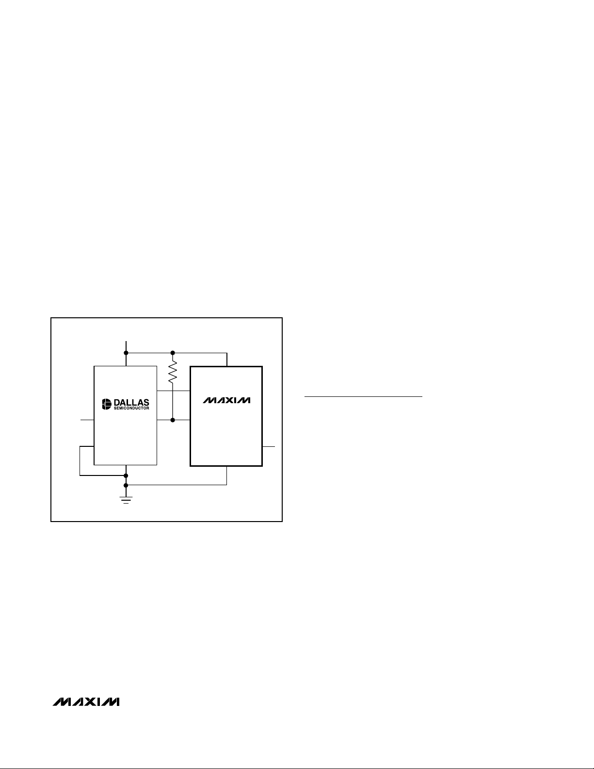
Temperature Sensor Outputs
Figure 11 shows the MAX6870/MAX6871 in a temperature-sensing application with the DS600. The DS600
generates an analog output voltage proportional to the
sensed temperature through V
OUT
and logic outputs on
TO and TO (only TO is shown). The internal ADC of the
MAX6870/MAX6871 digitizes the analog output voltage
of the DS600 and stores the results in read-only registers 5Ch through 5Fh. VTHsets the threshold voltage
that V
OUT
must exceed for TO to generate a logic-high
signal. VTHmust be less than 1.25V, otherwise the
overcurrent condition will occur after the internal ADC
attains its full-scale input voltage. Configure GPI1 as an
active-high input and configure PO7 (MAX6870)/PO5
(MAX6871) to depend on GPI1. When V
OUT
increases
above V
TH
, TO asserts high, causing PO7/PO5 to
assert to its active state.
Monitoring Other Voltages
Use AUXIN_ to monitor any voltage up to 1.25V. The
internal ADC of the MAX6870/MAX6871 digitizes the voltage and stores the results in read-only registers 5Ch
through 5Fh. The internal ADC cycles through the voltage monitor inputs and the auxiliary inputs every 200ms.
Layout and Bypassing
For better noise immunity, bypass each of the voltage
detector inputs to GND with 0.1µF capacitors installed
as close to the device as possible. Bypass ABP and
DBP to GND with 1µF capacitors installed as close to
the device as possible. ABP and DBP are internally
generated voltages and should not be used to supply
power to external circuitry.
Configuration Latency Period
A delay of less than 5µs occurs between writing to the
configuration registers and the time when these
changes actually take place, except when changing
one of the voltage-detector thresholds. Changing a
voltage-detector threshold typically takes 150µs. When
changing EEPROM contents, a software reboot or
cycling of power is required for these changes to transfer to volatile memory.
Chip Information
PROCESS: BiCMOS
MAX6870/MAX6871
EEPROM-Programmable Hex/Quad
Power-Supply Sequencers/Supervisors with ADC
______________________________________________________________________________________ 47
IN3
+5V
GND
AUXIN1
GPI1
CTG
V
TH
V
OUT
V
TH
(<1.25V)
TO
GND
V
DD
MAX6870
MAX6871
PO5/
PO3
DS600
R
PU
Figure 11. Temperature Sensor Outputs
Page 48

MAX6870/MAX6871
EEPROM-Programmable Hex/Quad
Power-Supply Sequencers/Supervisors with ADC
48 ______________________________________________________________________________________
32
31
30
29
28
27
26
PO1
REFIN
IN1
IN2
IN3
IN4
IN5
25 IN6
9
10
11
12
13
14
15
N.C.
N.C.
MARGIN
MR
SDA
SCL
A0
16A1
17
18
19
20
21
22
23
GPI4
*EXPOSED PADDLE INTERNALLY CONNECTED TO GND.
*EXPOSED PADDLE
GPI3
GPI2
GPI1
ABP
DBP
AUXIN2
8
7
6
5
4
3
2
PO8
PO7
PO6
PO5
GND
PO4
PO3
MAX6870
(7mm x 7mm Thin QFN)
1PO2
24 AUXIN1
TOP VIEW
32
31
30
29
28
27
26
N.C.
REFIN
IN1
IN2
IN3
IN4
N.C.
25 N.C.
9
10
11
12
13
14
15
N.C.
N.C.
MARGIN
MR
SDA
SCL
A0
16A1
17
18
19
20
21
22
23
GPI4
*EXPOSED PADDLE
GPI3
GPI2
GPI1
ABP
DBP
AUXIN2
8
7
6
5
4
3
2
N.C.
PO5
PO4
PO3
GND
PO2
PO1
MAX6871
(7mm x 7mm Thin QFN)
1N.C.
24 AUXIN1
Pin Configurations
Selector Guide
PART
VOLTAGE-
GENERAL-PURPOSE
INPUTS
PROGRAMMABLE
OUTPUTS
AUXILIARY
INPUTS
MAX6870ETJ 6 √ 48√
MAX6871ETJ 4 √ 45√
DETECTOR INPUTS
INTERNAL ADC
Page 49

MAX6870/MAX6871
EEPROM-Programmable Hex/Quad
Power-Supply Sequencers/Supervisors with ADC
______________________________________________________________________________________ 49
MAX6870
DC-DC
1
DBP
PO1
IN1
DC-DC
2
IN3
PO2
DC-DC
3
IN4
PO3
GND
IN5
PO5
IN6
PO4
IN2
SDA
SDA
+5V SWITCHED
+0.7V
+2.5V
+3.3V
+5V
+12V
µP
SCL
SCL
PO6
RESET
PO7
NMI, OV ALERT
PO8
A0
NMI, WD ALERT
GPI1
(WDI)
LOGIC OUTPUT
R
PU
R
PU
DC-DC
4
TEMP
SENSOR
+12V SUPPLY
PO1
PO2
PO3
+12V BUS INPUT
t
PO1
ENABLE +5V DC-DC CONVERTER
A1
GPI2 GPI4
GPI3
AUXIN1 REFIN
AUXIN2
ABP
MARGIN
MR
+12V
+5V SUPPLY
+5V OUTPUT
t
PO2
ENABLE +2.5V DC-DC CONVERTER
+2.5V SUPPLY
+2.5V OUTPUT
t
PO3
ENABLE +3.3V DC-DC CONVERTER
+3.3V SUPPLY
PO5
PO4
PO6
+3.3V OUTPUT
t
PO5
ENABLE +0.7V DC-DC CONVERTER
+0.7V SUPPLY
+0.7V OUTPUT
t
PO4
ENABLE +5V FET SWITCH
+5V SUPPLY
+5V SWITCHED OUTPUT
t
PO6
SYSTEM RESET
Typical Operating Circuit
Page 50

MAX6870/MAX6871
EEPROM-Programmable Hex/Quad
Power-Supply Sequencers/Supervisors with ADC
50 ______________________________________________________________________________________
Package Information
(The package drawing(s) in this data sheet may not reflect the most current specifications. For the latest package outline information,
go to www.maxim-ic.com/packages
.)
32, 44, 48L QFN.EPS
PROPRIETARY INFORMATION
APPROVAL
TITLE:
DOCUMENT CONTROL NO.
21-0144
PACKAGE OUTLINE
32, 44, 48, 56L THIN QFN, 7x7x0.8mm
1
D
REV.
2
e
L
e
L
A1AA2
E/2
E
D/2
D
DETAIL A
D2/2
D2
b
L
k
E2/2
E2
(NE-1) X e
(ND-1) X e
e
C
L
C
L
C
L
C
L
k
DALLAS
SEMICONDUCTOR
DETAIL B
e
L
L1
Page 51

MAX6870/MAX6871
EEPROM-Programmable Hex/Quad
Power-Supply Sequencers/Supervisors with ADC
Maxim cannot assume responsibility for use of any circuitry other than circuitry entirely embodied in a Maxim product. No circuit patent licenses are
implied. Maxim reserves the right to change the circuitry and specifications without notice at any time.
Maxim Integrated Products, 120 San Gabriel Drive, Sunnyvale, CA 94086 408-737-7600 ____________________ 51
© 2004 Maxim Integrated Products Printed USA is a registered trademark of Maxim Integrated Products.
Package Information (continued)
(The package drawing(s) in this data sheet may not reflect the most current specifications. For the latest package outline information,
go to www.maxim-ic.com/packages
.)
PROPRIETARY INFORMATION
DOCUMENT CONTROL NO.APPROVAL
TITLE:
REV.
2
2
21-0144
DALLAS
SEMICONDUCTOR
PACKAGE OUTLINE
32, 44, 48, 56L THIN QFN, 7x7x0.8mm
D
 Loading...