

Page 1
General Description
The MAX686 DAC-controlled boost/inverter IC converts
a positive input voltage to a positive or negative LCD
bias voltage up to +27.5V or -27.5V. The device features
an internal N-channel MOSFET switch, programmable
current limiting, and an internal 6-bit digital-toanalog converter (DAC) for digital adjustment of the
output voltage. It comes in a small 16-pin QSOP package (same size as an 8-pin SO).
The MAX686 uses a current-limited, pulse-frequencymodulation (PFM) control scheme to provide high efficiency over a wide range of load conditions. Its high
switching frequency (up to 300kHz) allows the use of
small external components.
An LCDON output allows the LCD bias voltage to be
automatically disabled when the display logic voltage is
removed, protecting the display. The MAX686 has a
+2.7V to +5.5V input voltage range for the IC, and a
+0.8V to +27.5V input voltage range for the inductor.
Typical quiescent supply current is 65µA. Shutdown
current is 1.5µA.
The MAX686 offers high-level integration to save space,
reduce power consumption, and increase battery life,
making it an excellent choice for battery-powered
portable equipment. The MAX629 is similar to the
MAX686, except that it does not contain a built-in DAC.
Both devices have evaluation kits to facilitate designs.
Applications
Positive or Negative LCD Bias
Personal Digital Assistants
Notebook Computers
Portable Data-Collection Terminals
Palmtop Computers
Varactor Tuning Diode Bias
____________________________Features
♦ Internal 500mA, 28V N-Channel Switch
(no external FET required)
♦ Adjustable Output Voltage to +27.5V or -27.5V
♦ 6-Bit DAC-Controlled Output Voltage
♦ Up to 90% Efficiency
♦ Small 16-Pin QSOP Package
(Same size as 8-pin SO)
♦ Power-OK Indicator
♦ 65µA Quiescent Current
♦ 1.5µA Shutdown Current
♦ Up to 300kHz Switching Frequency
MAX686
DAC-Controlled Boost/Inverter
LCD Bias Supply with Internal Switch
________________________________________________________________
Maxim Integrated Products
1
19-1327; Rev 1; 2/98
PART
MAX686C/D
MAX686EEE -40°C to +85°C
0°C to +70°C
TEMP. RANGE PIN-PACKAGE
Dice*
16 QSOP
EVALUATION KIT
AVAILABLE
Ordering Information
*
Dice are specified at TA= +25°C, DC parameters only.
For free samples & the latest literature: http://www.maxim-ic.com, or phone 1-800-998-8800.
For small orders, phone 408-737-7600 ext. 3468.
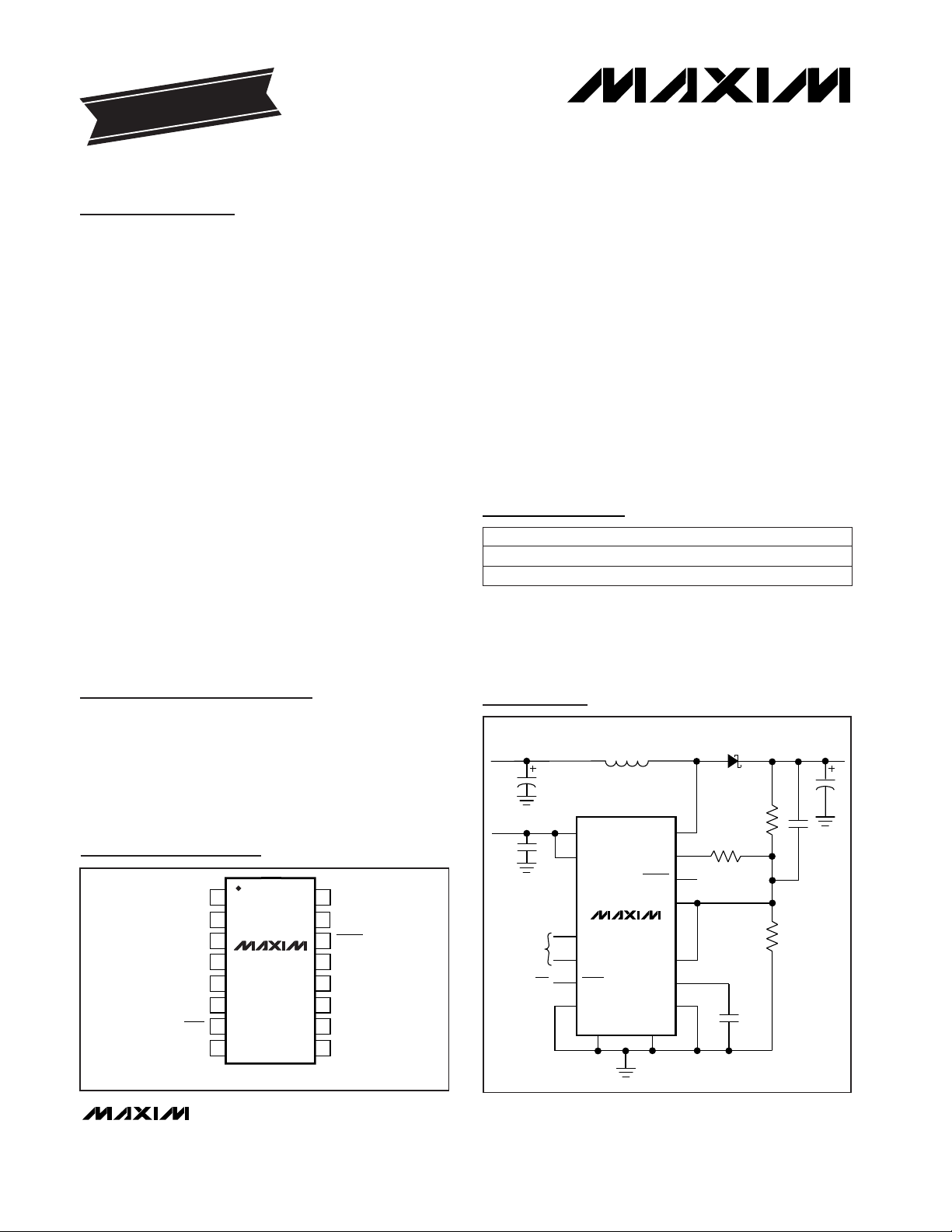
Functional Diagram appears at end of data sheet.
MAX686
V
CC
V
DD
V
OUT
22µH
V
IN
= 0.8V TO 27.5V
UP
SHDN
DN
POL
GND PGND
LX
DACOUT
LCDON
FB
REF
POK
ISET
0.1µF
R3
R2
MBR0530L
R1
ON/OFF
DAC CONTROL
V
CC
= 2.7V TO 5.5V
0.1µF
Typical Operating Circuit
16
15
14
13
12
11
10
9
1
2
3
4
5
6
7
8
PGND LX
N.C.
LCDON
GND
POK
FB
REF
TOP VIEW
MAX686
QSOP
UP
DN
ISET
POL
V
DD
V
CC
SHDN
DACOUT
Pin Configuration
Page 2
MAX686
DAC-Controlled Boost/Inverter
LCD Bias Supply with Internal Switch
2 _______________________________________________________________________________________
ABSOLUTE MAXIMUM RATINGS
ELECTRICAL CHARACTERISTICS
(VCC= VDD= VIN= +5V, C
REF
= 0.1µF, TA= 0°C to +85°C, unless otherwise noted. Typical values are at TA= +25°C.)
Stresses beyond those listed under “Absolute Maximum Ratings” may cause permanent damage to the device. These are stress ratings only, and functional
operation of the device at these or any other conditions beyond those indicated in the operational sections of the specifications is not implied. Exposure to
absolute maximum rating conditions for extended periods may affect device reliability.
Voltage
V
CC
, ISET, POK, POL, SHDN,
UP, DN, V
DD
to GND...........................................-0.3V to +6V
FB, REF, DACOUT to GND.......................-0.3V to (V
CC
+ 0.3V)
PGND to GND .....................................................-0.3V to +0.3V
LX, LCDON to GND..............................................-0.3V to +30V
Current
LX (sinking).....................................................................600mA
LCDON (sinking)...............................................................10mA
Continuous Power Dissipation (T
A
= +70°C)
QSOP (derate 8.30mW/°C above +70°C)......................667mW
Operating Temperature Ranges
MAX686C/D ..........................................................0°C to +70°C
MAX686EEE.......................................................-40°C to +85°C
Storage Temperature Range.............................-65°C to +160°C
Lead Temperature (soldering, 10sec).............................+300°C
SHDN = GND
POL = GND, VFB= 1.3V, I
DACOUT
= 0mA
Boost configuration, V
OUT
= 27.5V,
I
LOAD
= 0mA to 5mA
Boost configuration, V
OUT
= 27.5V,
I
LOAD
= 5mA, VCC= V
DD
= 2.7V to 5.5V
Rising or falling
CONDITIONS
µA
1.3 4
I
SHDN
Shutdown Current
µA
65 125
ICC+ I
DD
V
2.7 5.5
VCC, V
DD
Supply Voltage (Note 1)
Supply Current
V
28
V
LX
LX Voltage Range
%/mA
0.01
Load Regulation
%/V
0.1
Line Regulation
V
2.10 2.5 2.65
V
LOCK
VCCUndervoltage Lockout
mV
100
VCCUndervoltage Lockout
Hysteresis
V
0.5 1.5 2.1
V
RESET
VCCDAC Reset Threshold
UNITSMIN TYP MAXSYMBOLPARAMETER
ISET = V
CC
A
0.42 0.50 0.58
I
LX
LX Switch Current Limit
ISET = GND
0.21 0.25 0.29
VLX= 28V µA
1.5
I
LXLEAK
LX Leakage Current
VCC= V
DD
= 5V, ILX= 100mA
Ω
0.6 1.2
R
LX
LX On-Resistance
VCC= V
DD
= 3.3V, ILX= 100mA
0.8 1.6
µs
8 10 12
t
ON
Maximum LX On-Time
POL = GND, VFB> 1.2V
µs
0.8 1 1.2
t
OFF
Minimum LX Off-Time
POL = VCC, VFB< 0.15V
2.8 3.5 4.2
POL = GND, VFB< 0.8V
4 5 6
POL = VCC, VFB> 0.4V
4 5 6
Voltage applied to L1 V
0.8 V
OUT
V
IN
Input Voltage
LX
Page 3
MAX686
DAC-Controlled Boost/Inverter
LCD Bias Supply with Internal Switch
_______________________________________________________________________________________ 3
I
REF
= 0µA to 25µA, C
REF
= 0.1µF
VCC= VDD= 2.7V to 5.5V, no load
0µA < I
DACOUT
< 20µA
-50µA < I
DACOUT
< 0µA
I
REF
= 0µA to 50µA, C
REF
= 0.47µF
CONDITIONS
mV
1 10
REF Load Regulation
V
1.225 1.250 1.275
V
REF
REF Output Voltage
mV
0 15
V
ZS
Zero-Scale Output Voltage
V
V
REF
-
V
REF
V
REF
+
0.015 0.015
V
FS
Full-Scale Output Voltage
1.5
nA
±50
I
FB
FB Input Bias Current
UNITSMIN TYP MAXSYMBOLPARAMETER
ELECTRICAL CHARACTERISTICS (continued)
(VCC= VDD= VIN= +5V, C
REF
= 0.1µF, TA= 0°C to +85°C, unless otherwise noted. Typical values are at TA= +25°C.)
POL = GND
POL = V
CC
V
1.225 1.250 1.275
V
FB
FB Set Point
mV
-15 0 15
nA
±50
I
POK
POK Input Current
V
POK
rising V
1.100 1.125 1.150
V
POK
POK Threshold
mV
12
POK Hysteresis
V
LCDON
= 0.4V, V
POK
= 1.25V mA
2 6
I
LCDON
LCDON Sink Current
V
LCDON
= 28V, V
POK
= GND µA
0.02 1
LCDON Leakage Current
bits
6
Resolution
Mid-scale = V
REF
x 32/63 %
-2 2
MSAMid-Scale Accuracy
Guaranteed monotonic LSB
-1 1
DNLDifferential Nonlinearity
kΩ
1.5
R
DACOUT
Output Resistance in Shutdown
2.7V < VCC= VDD< 5.5V V0.7V
IL
Input Low Level
2.7V < VCC= VDD< 5.5V V2.4V
IH
Input High Level
µA±1I
BIAS
Input Bias Current
UP, DN, TA= +25°C µs1t
PWH
Pulse Width High
UP, DN, TA= +25°C µs1t
PWL
Pulse Width Low
UP, DN, TA= +25°C µs1t
PWS
Pulse Separation
REFERENCE AND FB INPUT
POWER OK COMPARATOR, LCDON OUTPUT
DAC OUTPUT (Notes 2, 3)
LOGIC INPUTS: POL, ISET, UP, DN, SHDN
Page 4
MAX686
DAC-Controlled Boost/Inverter
LCD Bias Supply with Internal Switch
4 _______________________________________________________________________________________
ISET = V
CC
A
0.4 0.6
SHDN = GND
I
LX
LX Switch Current Limit
POL = GND, VFB = 1.3V, I
DACOUT
= 0mA
ISET = GND
VCC= VDD= 5V, ILX= 100mA
0.2 0.3
Ω
1.2
VLX= 28V
Rising or falling
µA
1.5
CONDITIONS
I
LXLEAK
LX Leakage Current
R
LX
LX On-Resistance
VCC= VDD= 3.3V, ILX= 100mA
1.6
µs
7.5 12.5
t
ON
Maximum LX On-Time
POL = GND, VFB> 1.2V
µs
0.7 1.3
t
OFF
Minimum LX Off-Time
POL = VCC, VFB< 0.15V
2.8 4.2
POL = GND, VFB< 0.8V
3.8 6.2
POL = VCC, VFB> 0.4V
3.8 6.2
µA
4
I
SHDN
Shutdown Current
µA
125
ICC+ I
DD
V
2.7 5.5
VCC, V
DD
Supply Voltage (Note 1)
Supply Current
V
28
V
LX
LX Voltage Range
V
2.10 2.65
V
LOCK
VCCUndervoltage Lockout
UNITSMIN TYP MAXSYMBOLPARAMETER
ELECTRICAL CHARACTERISTICS
(VCC= VDD= VIN= +5V, C
REF
= 0.1µF, TA= -40°C to +85°C, unless otherwise noted.) (Note 4)
Note 1: The MAX686 requires a supply voltage at V
CC
= VDDbetween +2.7V and +5.5V; however, the voltage that supplies the
inductor can vary from +0.8V to +27.5V, depending on circuit operating conditions.
Note 2: The DAC output is set to its midpoint value at power-on.
Note 3: The DAC setting is guaranteed to remain valid as long as V
CC
is greater than the V
CC
DAC Reset Threshold.
Note 4: Specifications to -40°C are guaranteed by design, not production tested.
VCC= VDD= 2.7V to 5.5V, no load V
1.22 1.28
V
REF
REF Output Voltage
I
REF
= 0µA to 25µA, C
REF
= 0.1µF mV
10
REF Load Regulation
POL = GND V
1.22 1.28
V
FB
FB Set Point
POL = V
CC
-15 15
nA
±50
I
FB
FB Input Bias Current
V
POK
rising V
1.05 1.20
V
POK
POK Threshold
nA
±50
I
POK
POK Input Current
V
LCDON
= 0.4V, V
POK
= 1.25V mA
2
I
LCDON
LCDON Sink Current
mV
Voltage applied to L1 V
0.8 V
OUT
V
IN
Input Voltage
-50µA < I
DACOUT
< 0µA V
V
REF
- V
REF
+
0.02 0.02
V
FS
Full-Scale Output Voltage
0µA < I
DACOUT
< 20µA mV
0 15
V
ZS
Zero-Scale Output Voltage
Bits
6
Resolution
Mid-scale = V
REF
x 32/63 %
-3 3
MSAMid-Scale Accuracy
2.7V < VCC= V
DD
< 5.5V V
0.7
V
IL
Input Low Level
2.7V < VCC= V
DD
< 5.5V V
2.4
V
IH
Input High Level
µA
±1
I
BIAS
Input Bias Current
LX
REFERENCE AND FB INPUT
POWER OK COMPARATOR, LCDON OUTPUT
LOGIC INPUTS: POL, ISET, UP, DN, SHDN
DAC OUTPUT (Notes 2, 3)
Page 5
MAX686
DAC-Controlled Boost/Inverter
LCD Bias Supply with Internal Switch
_______________________________________________________________________________________ 5
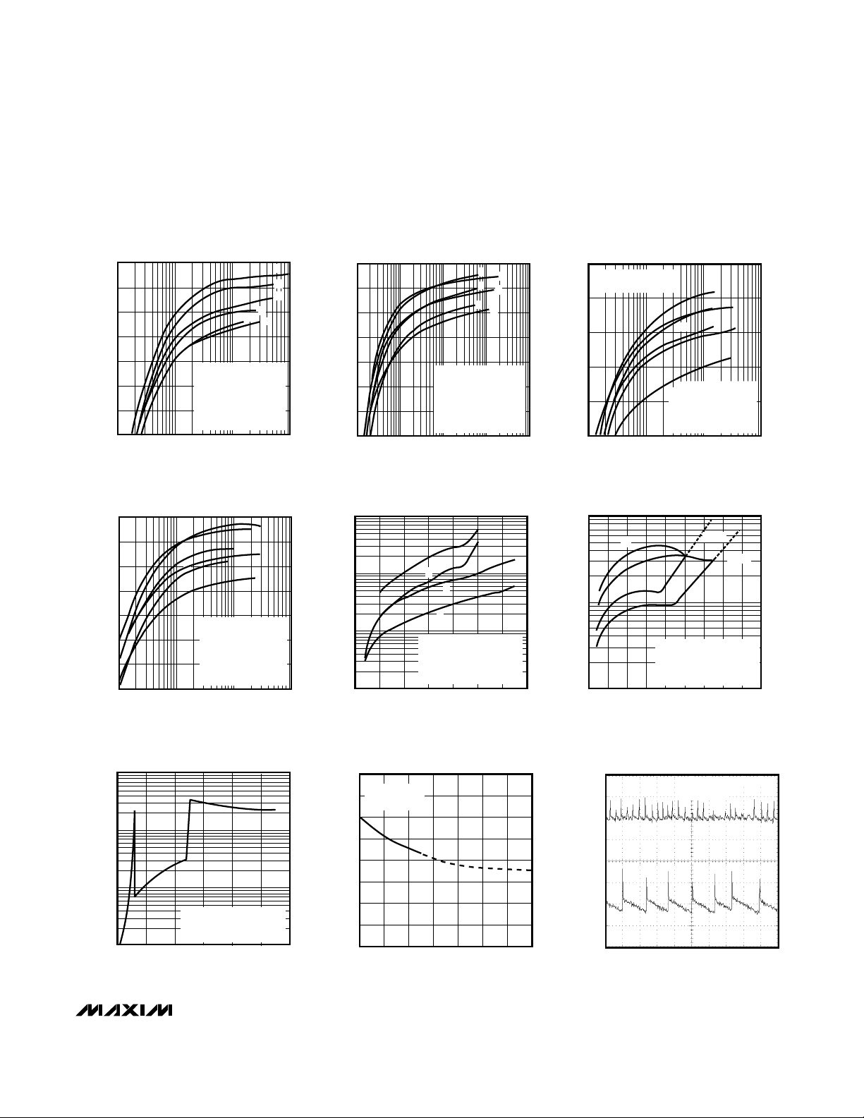
95
60
0.1 1 10 100
EFFICIENCY vs. LOAD CURRENT
(V
OUT
= +24V)
70
65
75
80
85
90
MAX686 TOC01
LOAD CURRENT (mA)
EFFICIENCY (%)
A: VIN = 12V, ISET = V
CC
B: VIN = 12V, ISET = GND
C: V
IN
= 5V, ISET = V
CC
D: VIN = 5V, ISET = GND
E: V
IN
= 3V, ISET = GND
F: V
IN
= 3V, ISET = V
CC
C
D
E
F
A
B
95
90
60
0.1 101 1000100
EFFICIENCY vs. LOAD CURRENT
(V
OUT
= +12V)
65
MAX686 TOC02
LOAD CURRENT (mA)
EFFICIENCY (%)
70
75
80
85
A: VIN = 9V, ISET = V
CC
B: VIN = 9V, ISET = GND
C: V
IN
= 5V, ISET = V
CC
D: VIN = 5V, ISET = GND
E: V
IN
= 3V, ISET = GND
F: V
IN
= 3V, ISET = V
CC
D
C
F
B
A
E
85
60
0.1 1 10 100
EFFICIENCY vs. LOAD CURRENT
(V
OUT
= -12V)
65
70
75
80
MAX686 TOC03
LOAD CURRENT (mA)
EFFICIENCY (%)
A
F
E
B
D
C: V
IN
= 5V, ISET = GND
D: V
IN
=
5V, ISET = V
CC
E: V
IN
=
3V, ISET = GND
F: V
IN
= 3V, ISET = V
CC
A: V
IN
= 9V, ISET = GND
B: V
IN
= 9V, ISET = V
CC
C
__________________________________________Typical Operating Characteristics
(Circuits of Figures 1 and 2, VCC= VDD= VIN= +5V, L1 = 22µH, SHDN = VCC, C
REF
= 0.1µF, TA= +25°C, unless otherwise noted.)
85
50
0.1 1 10 100
EFFICIENCY vs. LOAD CURRENT
(V
OUT
= -18V)
60
55
65
70
75
80
MAX686 TOC04
LOAD CURRENT (mA)
EFFICIENCY (%)
C
D
A: VIN = 9V, ISET = GND
B: V
IN
= 9V, ISET = V
CC
C: VIN = 5V, ISET = GND
D: V
IN
= 5V, ISET = V
CC
E: VIN = 3V, ISET = GND
F: V
IN
= 3V, ISET = V
CC
E
F
A
B
1000
1
0 4 62 10 128 14
MAXIMUM OUTPUT CURRENT vs.
INPUT VOLTAGE (V
OUT
= +12V, +24V)
10
100
MAX686 TOC05
INPUT VOLTAGE (V)
OUTPUT CURRENT (mA)
A: V
OUT
= 12V, ISET = V
CC
B: V
OUT
= 12V, ISET = GND
C: V
OUT
= 24V, ISET = V
CC
D: V
OUT
= 24V, ISET = GND
A
C
D
B
1
10
100
0 4 6 82 10 12 14 16 18
MAXIMUM OUTPUT CURRENT vs.
INPUT VOLTAGE (V
OUT
= -12V, -18V)
MAX686 TOC06
INPUT VOLTAGE (V)
OUTPUT CURRENT (mA)
B
D
C
A: V
OUT
= -12V, ISET = V
CC
B: V
OUT
= -18V, ISET = V
CC
C: V
OUT
= -12V, ISET = GND
D: V
OUT
= -18V, ISET = GND
A
B & D
A & C
V
OUT
50mV/div
AC-COUPLED
V
OUT
50mV/div
AC-COUPLED
ISET = V
CC
ISET = GND
OUTPUT VOLTAGE RIPPLE
MAX686 TOC09
20µs/div
V
OUT
= 24V
I
LOAD
= 5mA
1000
1
0 21 4 53 6
INPUT CURRENT
vs. INPUT VOLTAGE
10
100
MAX686 TOC07
INPUT VOLTAGE (V)
INPUT CURRENT (µA)
VCC = V
IN
= V
DD
INPUT CURRENT = ICC + I
DD
V
OUT
= 18V, NO LOAD
1.244
1.246
1.245
1.248
1.247
1.251
1.250
1.249
1.252
0 4020 60 80 100 120 140
REFERENCE VOLTAGE
vs. LOAD CURRENT
MAX686 TOC08
LOAD CURRENT (µA)
REFERENCE VOLTAGE (V)
VIN = VCC = 5V
C
REF
= 0.1µF
Page 6

MAX686
DAC-Controlled Boost/Inverter
LCD Bias Supply with Internal Switch
6 _______________________________________________________________________________________
_____________________________Typical Operating Characteristics (continued)
(Circuits of Figures 1 and 2, VCC= VDD= VIN= +5V, L1 = 22µH, SHDN = VCC, C
REF
= 0.1µF, TA= +25°C, unless otherwise noted.)
V
OUT
50mV/div
AC-COUPLED
3V
5V
LINE-TRANSIENT RESPONSE
(ISET = V
CC
)
MAX686 TOC10
5ms/div
V
CC
= V
DD =VIN
V
OUT
50mV/div
AC-COUPLED
3V
5V
LINE-TRANSIENT RESPONSE
(ISET = GND)
MAX686 TOC10A
5ms/div
V
OUT
= 24V
I
LOAD
= 5mA
V
CC
= V
DD
= V
IN
V
OUT
I
OUT
20mV/div
AC-COUPLED
100µA
5mA
LOAD-TRANSIENT RESPONSE
(ISET = GND)
MAX686 TOC11
2ms/div
V
OUT
= 24V
V
OUT
I
OUT
50mV/div
AC-COUPLED
100µA
5mA
LOAD-TRANSIENT RESPONSE
(ISET = V
CC
)
MAX686 TOC12
2ms/div
V
OUT
= 24V
V
OUT
5V/div
5V
18.7V
POWER-UP RESPONSE
(POSITIVE CONFIGURATION)
MAX686 TOC13A
500µs/div
SHDN
2V/div
I
SET
= V
CC
RL = 4.7kΩ
V
OUT
5V/div
5V
18.7V
POWER-DOWN RESPONSE
(POSITIVE CONFIGURATION)
MAX686 TOC13B
5ms/div
SHDN
2V/div
I
SET
= V
CC
RL = 4.7kΩ
Page 7

MAX686
DAC-Controlled Boost/Inverter
LCD Bias Supply with Internal Switch
_______________________________________________________________________________________ 7
_____________________________Typical Operating Characteristics (continued)
(Circuits of Figures 1 and 2, VCC= VDD= VIN= +5V, L1 = 22µH, SHDN = VCC, C
REF
= 0.1µF, TA= +25°C, unless otherwise noted.)
V
OUT
5V/div
-16.8V
0V
POWER-UP RESPONSE
(NEGATIVE CONFIGURATION)
MAX686 TOC14A
500µs
SHDN
5V/div
I
SET
= V
CC
RL = 4.7kΩ
V
OUT
5V/div
-16.8V
0V
POWER-DOWN RESPONSE
(NEGATIVE CONFIGURATION)
MAX686 TOC14B
20ms/div
SHDN
5V/div
I
SET
= V
CC
RL = 4.7kΩ
Reference Output. Bypass with a 0.1µF ceramic capacitor to GND.REF9
Feedback Input. Connect to an external voltage divider to set the MAX686 output voltage. See the section
Setting the Output Voltage with the DAC
.
FB10
Power-OK Sense Input/Power-OK Comparator Input. When the voltage applied to POK is greater than
1.125V, LCDON is low. Connect to a resistive voltage divider monitoring V
IN
or V
OUT
.
POK11
IC Power-Supply InputV
CC
12
GroundGND13
Gate-Drive Supply for Internal MOSFET. Connect to VCC.V
DD
5
Set LX Current Limit. Sets the peak current limit for the internal switch. Connect to VCCfor 500mA current
limit. Connect to GND for 250mA current limit.
ISET6
Shutdown Input. A logic low on SHDN places the MAX686 in shutdown mode. Connect to VCCfor normal
operation.
SHDN
7
DAC Output VoltageDACOUT8
Polarity Input. Changes polarity and threshold of FB to allow regulation of either positive or negative output
voltages. POL also changes the polarity of the DAC output such that increasing codes always increases the
magnitude of the output voltage. Set POL = GND for positive output voltage, or set POL = VCCfor negative
output voltage.
POL4
Decrement Output Voltage Input. Decrements the DAC on each rising edge such that |V
OUT
|
decreases.
DN3
PIN
Increment Output Voltage Input. Increments the DAC on each rising edge such that |V
OUT
|
increases.
UP2
Power Ground. Connect to GND.PGND1
FUNCTIONNAME
Power-OK Comparator Open-Drain Output. Connect to external switch to turn LCD power on or off. See the
section
Controlling the LCD Using POK and LCDON
.
LCDON
14
No Connection. Not internally connected.N.C.15
Drain of Internal 28V, 500mA N-Channel SwitchLX16
Pin Description
Page 8

MAX686
DAC-Controlled Boost/Inverter
LCD Bias Supply with Internal Switch
8 _______________________________________________________________________________________
MAX686
V
CC
V
DD
V
OUT
C
F
22pF
V
IN
= 0.8V TO 27.5V
UP
SHDN
DN
POL
GND PGND
LX
L1
22µH
DACOUT
LCDON
FB
REF
POK
ISET
0.1µF
R3
R2
D1
MBR0530L
R1
ON/OFF
DAC CONTROL
15µF
4.7µF
V
CC
= 2.7V TO 5.5V
0.1µF
0.1µF
Figure 1. Boost Configuration: Positive Output Voltage
MAX686
V
CC
V
DD
V
IN
≤ |V
OUT|
≤ 27.5V
MBRO530L
D2
MBRO530L
NEGATIVE
OUTPUT
VOLTAGE
V
IN
= 0.8V TO 27.5V
UP
POL
SHDN
DN
GND PGND
LX
DACOUT
LCDON
FB
REF
POK
ISET
0.1µF
2.2µF
L1
22µH
D1
R4
2Ω
2.2µF
R3
R2R1
ON/OFF
DAC CONTROL
C
F
100pF
V
CC
= 2.7V TO 5.5V
0.1µF
15µF
Figure 2. Negative Output Voltage Application Circuit
Page 9

MAX686
DAC-Controlled Boost/Inverter
LCD Bias Supply with Internal Switch
_______________________________________________________________________________________ 9
Figure 3. Alternative Negative Output Voltage Application Circuit
MAX686
V
CC
V
DD
|V
OUT
| ≤ (27.5V - V
IN
)
D1
MBR0530L
D2
MBR0530L
L1
22µH
R4
2Ω
NEGATIVE
OUTPUT
VOLTAGE
V
IN
= 0.8V TO 27.5V
UP
POL
SHDN
DN
GND PGND
LX
DACOUT
LCDON
FB
REF
POK
ISET
0.1µF
2.2µF
2.2µF
R3
R2R1
ON/OFF
DAC CONTROL
C
F
470pF
V
CC
= 2.7V TO 5.5V
0.1µF
15µF
Detailed Description
The MAX686 is a step-up converter that contains an
internal N-channel MOSFET switch to convert a +0.8V
to +27.5V battery voltage to a higher positive or a negative voltage. Figure 1 shows the MAX686 configured to
produce a positive output voltage. Figure 2 shows the
MAX686 configured with one additional diode and
capacitor to produce a negative output voltage. Figure
3 shows an alternative method for developing negative
output voltages. Set the output voltage with an external
resistor-divider network. Adjust the output voltage with
the internal digital-to-analog converter (DAC). The
MAX686’s current-limited pulse-frequency-modulation
(PFM) control scheme has programmable current limiting and provides high efficiency over a wide range of
load conditions.
Boost Control Scheme (POL = GND)
A combination of peak current limiting and a pair of oneshots controls the MAX686 switching. During the oncycle, the internal switch closes, and current through
the inductor ramps up until either the fixed 10µs maximum on-time expires (at low input voltages) or the
switch peak current limit is reached. The peak current
limit is selectable to either 500mA (ISET = VCC) or
250mA (ISET = GND) (see the section
Setting the Peak
Inductor Current Limit
).
After the on-cycle terminates, the switch turns off, and
the inductor charges the output capacitor through the
diode. If the output is out of regulation after the minimum off-time has transpired, another on-cycle begins.
If the output is within regulation when the minimum offtime transpires, the off-cycle extends until the output
falls out of regulation, at which point an on-cycle starts.
The MAX686 regulates the voltage on FB (V
FB
) to
1.25V. When the output is well below regulation (V
FB
is
less than 1V and the switch current limit is exceeded),
the MAX686 operates in initial power-up mode, and the
minimum off-time increases to 5µs to provide soft-start.
The switching frequency, which depends on the load,
the input voltage, and the output voltage, can be as
high as 300kHz.
Inverting Control Scheme (POL = VCC)
In inverting operation, the MAX686 regulates the voltage on FB (VFB) to 0V, and the error amplifier’s polarity
is reversed. The minimum off-time changes to 3.5µs for
negative output voltages. When the output is well below
regulation (VFBis 0.25V or more and the switch current
limit is exceeded), initial power-up is assumed, and the
minimum off-time increases to 5µs to provide soft-start.
Page 10

MAX686
DAC-Controlled Boost/Inverter
LCD Bias Supply with Internal Switch
10 ______________________________________________________________________________________
Power-OK Comparator
POK is the input to the power-OK comparator. The
comparator drives an internal N-channel MOSFET. The
MOSFET’s open-drain output, LCDON, can drive an
external PNP transistor or P-channel MOSFET, switching a positive V
OUT
to the LCD (Figures 6 and 7). When
the voltage at POK exceeds 1.125V (power OK),
LCDON goes low, turning on the external PNP transistor. When the voltage at POK drops below 1.125V
(power not OK), the external PNP transistor turns off,
cutting off power to the LCD display. This feature
ensures that the LCD display is not damaged due to
improper voltage levels. During shutdown or undervoltage lockout, LCDON is high impedance.
Shutdown Mode
When SHDN is low, the MAX686 enters shutdown
mode, in which the control circuit, POK comparator,
DAC output buffer, reference, and internal biasing circuitry turn off. The DAC setting is stored as long as V
CC
remains above the DAC reset threshold. Supply current
drops to 1.5µA. SHDN is a logic-level input; connect it
to V
CC
for normal operation.
The output voltage in shutdown mode depends on the
output voltage polarity. In the positive output voltage
configuration (Figure 1), the output is directly connected to the input through the diode (D1) and the inductor
(L1). When the device is in shutdown mode, the output
voltage falls to one diode drop below the input voltage,
and any load connected to the output may still conduct
current. In the negative output voltage configuration
(Figures 2 and 3), there is no DC path between the
input and the output, and the output falls to GND in
shutdown mode.
Internal DAC
The MAX686 contains an internal 6-bit counter and
DAC to control the output voltage digitally (see the section
Setting the Output Voltage with the DAC
). The UP
and DN input pins drive an internal up/down counter
that directly controls the DAC. To increase the magnitude of V
OUT
in the boost configuration, apply a rising
edge to UP. This decreases the DAC output voltage
one step and correspondingly increases V
OUT.
Conversely, to decrease the magnitude of V
OUT
, apply
a rising edge to DN. This increases the DAC output
voltage one step and correspondingly decreases
V
OUT
. The UP and DN control direction reverses for a
negative output to maintain the same control direction of
the absolute magnitude of the output voltage. Upon
power-up, the DAC code internally goes to mid-scale.
The DAC’s internal counter does not roll over once it
reaches full scale or zero. Therefore, additional rising
edges to make the counter roll over are ignored, preventing unexpected undervoltages or overvoltages.
Internal Reference
The MAX626’s 1.25V internal reference is accurate to
±2% over temperature. It can source up to 50µA of current and should be bypassed with at least a 0.1µF
capacitor. See the
Bypass Capacitors
section.
Design Procedure
Setting the Output Voltage with the DAC
For either positive or negative output voltage applications, set the MAX686’s output voltage using three external resistors (R1, R2, and R3) as shown in Figures 1, 2,
and 3. Since the input bias current at FB has a 50nA
maximum value, large resistors can be used in the
feedback loop without a significant loss of accuracy.
Select R1 to be in the 10kΩ to 220kΩ range and calculate R2 and R3 using the applicable equations from the
following subsections.
Setting the Minimum Positive Output Voltage
The minimum output voltage is set with the resistordivider (R1-R2, Figure 1) from V
OUT
to FB. The mini-
mum output voltage occurs when V
DACOUT
= VFB=
1.25V. Therefore, R3 has no effect on the minimum output voltage. Choose R1 to be 120kΩ so that the current
in the divider is about 10µA. Then determine R2 as follows:
R2 = R1 x (V
OUT(MIN
)
- VFB) / V
FB
For example, if V
OUT(MIN)
= 12.5V:
R2 = 120kΩ x (12.5 - 1.25) / (1.25) =1.08MΩ
Mount R1 and R2 close to the FB pin to minimize parasitic capacitance.
Setting the Maximum Positive Output Voltage
The DAC is adjustable from 0V to 1.25V in 64 steps,
and 1LSB = 1.25V / 63 = 19.8mV. Calculate R3 to
adjust V
OUT
with DACOUT (Figure 1).
For V
OUT(MAX)
= 25V and V
OUT(MIN)
= 12.5V, deter-
mine R3 as follows:
R3 = R2 x (V
FB
) / (V
OUT(MAX
) - V
OUT(MIN)
)
= 1.08MΩ x (1.25) / (25 - 12.5) = 108kΩ
The general form for V
OUT
as a function of the DAC out-
put (V
DACOUT
) is:
V
OUT
= V
OUT(MIN)
+ (VFB- V
DACOUT
) x R2 / R3
At power-up, the DAC resets to mid-scale where
V
DACOUT
= 0.635V. Therefore, the output voltage after
power-up is:
V
OUT(MID)
= V
OUT(MIN)
+ (1.25 - 0.635) x
R2 / R3 = 18.65V
Page 11

MAX686
DAC-Controlled Boost/Inverter
LCD Bias Supply with Internal Switch
______________________________________________________________________________________ 11
Note that for a positive output voltage, V
OUT
increases
as V
DACOUT
decreases. V
OUT(MAX)
corresponds to
V
DACOUT
= 0V, and V
OUT(MIN)
corresponds to
V
DACOUT
= 1.25V.
Setting the Minimum Negative Output Voltage
For a negative output voltage, the FB threshold voltage
(VFB) is 0V, and R1 is placed between FB and REF
(Figures 2 and 3). Again, choose R1 to be 120kΩ so
that the current in the divider is about 10µA. Then
determine R2 as follows:
R2 = R1 x |V
OUT
/ V
REF
|
For example, if V
OUT(MIN)
= -12.5V:
R2 = 120kΩ x |(-12.5) / (1.25)| = 1.2MΩ
Setting the Maximum Negative Output Voltage
Assume V
OUT(MAX)
= -25V and V
OUT
(MIN)
= -12.5V,
then determine R3 and V
OUT(MID)
as follows:
R3 = R2 x (VFB- V
DACOUT(MAX)
) / (V
OUT(MAX)
-
V
OUT(MIN)
)
= 1.2MΩ x (0 - 1.25) / (-25 - -12.5) =120kΩ
For a negative output voltage,
V
OUT
= V
OUT(MIN)
+ (VFB- V
DACOUT
) x R2 / R3.
At power-up, the DAC resets to mid-scale where V
DACOUT
= 0.635V. Therefore, the output voltage after reset is:
V
OUT(MID)
= -12.5 + (0 - 0.635) x (1.2M) /
(120k) = -18.85V
Note that for a negative output voltage, |V
OUT
| increas-
es as V
DACOUT
increases. |V
OUT(MAX)
| corresponds to
V
DACOUT
= 1.25V, and |V
OUT(MIN)
| corresponds to
V
DACOUT
= 0V.
Setting the Output Voltage
without the DAC
The MAX686 may be used without the DAC to control
the output voltage. For either positive or negative output voltage applications, set the MAX686’s output voltage using only two external resistors (R1 and R2) as
shown in Figure 1, 2, or 3. Since the input bias current
at FB has a 50nA maximum value, large resistors can
be used in the feedback loop without a significant loss
of accuracy. Select R1 to be in the 10kΩ to 220kΩ
range and calculate R2 using the applicable equations
from the following subsections.
Setting the Positive Output Voltage
Use the circuit of Figure 1, connecting POL to GND and
omitting R3. Connecting POL to GND sets the threshold
voltage at FB to V
REF
. Choose the value of R1 in the
10kΩ to 220kΩ range and calculate R2 as follows:
R2 = R1 x
(V
OUT
/ V
REF
-1)
where V
REF
= 1.25V.
Setting the Negative Output Voltage
For negative output voltages, configure R1 and R2 as
shown in Figures 2 and 3, connecting POL to VCCand
omitting R3. Connecting POL to VCCsets the FB threshold voltage to GND for negative output voltages.
Choose R1 in the 10kΩ to 220kΩ range and calculate
R2 as follows:
R2 = R1 x |V
OUT
|/ V
REF
where V
REF
= 1.25V.
Figures 2 and 3 demonstrate two possible methods of
generating a negative voltage with the MAX686. In
Figure 3, D2 connects to the input supply (V
IN
). This
connection features the best output ripple performance, but |V
OUT
|
must be limited to values less than
-27.5V - VIN. If the application requires a larger negative voltage, use the method of Figure 2, connecting D2
to GND. This method allows a maximum output voltage
of -27.5V, but |V
OUT
|
must be greater than VIN.
Setting the Peak Inductor Current Limit
External current-limit selection provides added control
over the MAX686’s output performance. A higher current limit increases the amount of energy stored in the
inductor during each cycle, which provides higher output current capability. For higher output current applications, choose the 500mA current-limit option by
connecting ISET to VCC. When the load requires lower
output current, the 250mA current limit provides several
advantages. First, a smaller inductor saves board area
and cost. Second, smaller energy transfers per cycle
reduce output ripple for a given capacitor. Connecting
ISET to GND selects the 250mA current-limit option.
Connecting ISET to VCCselects the 500mA current-limit
option. Refer to the
Typical Operating Characteristics
for efficiency and load current graphs at each ISET current setting.
Selecting Inductors
The MAX686’s high switching frequency allows for the
use of a small inductor. The 22µH inductor shown in
Figures 1, 2, and 3 is recommended for most applications, although values between 10µH and 47µH are
acceptable. Use inductors with a ferrite core or equivalent; powder iron cores are not recommended for use
with high switching frequencies. The inductor’s incremental saturation rating must exceed the selected current limit. For highest efficiency, use an inductor with a
low DC resistance (under 200mΩ). See Table 1 for a list
of inductor suppliers.
Page 12

MAX686
DAC-Controlled Boost/Inverter
LCD Bias Supply with Internal Switch
12 ______________________________________________________________________________________
Selecting Diodes
The MAX686’s high switching frequency demands a
high-speed rectifier. Schottky diodes, such as the
1N5818 or MBR0530L, are recommended. Make sure
that the diode’s peak current rating exceeds the peak
current set by ISET and that its breakdown voltage
exceeds the output voltage. Schottky diodes are preferred due to their low forward voltage. However, ultrahigh-speed silicon rectifiers are also acceptable. Table 1
lists Schottky diode suppliers.
Selecting Capacitors
Output Filter Capacitors
The primary selection criterion for the output filter
capacitor is low equivalent series resistance (ESR). The
product of the peak inductor current and the output filter capacitor’s ESR determines the amplitude of the
high-frequency ripple seen on the output voltage.
These requirements can be balanced by appropriately
selecting the current limit, as discussed in the
Setting
the Peak Inductor Current Limit
section. Table 1 lists
some low-ESR capacitor suppliers.
Bypass Capacitors
Although the output current of many MAX686 applications may be relatively small, the input supply must be
able to source current transients equal to the ISET current limit. The input bypass capacitor reduces the peak
currents drawn from the voltage source and reduces
noise caused by the MAX686’s switching action. The
input source impedance determines the size of the
capacitor required at the input (VIN). As with the output
filter capacitor, low ESR is the primary consideration. A
15µF, low-ESR capacitor is adequate for most applications, although smaller bypass capacitors may also be
acceptable in light-load applications. Bypass the IC
separately with a 0.1µF ceramic capacitor placed as
close as possible to the VCCand GND pins.
Bypass REF to GND with a 0.1µF ceramic capacitor for
REF currents up to 25µA. REF can source up to 50µA of
current for external loads. For 25µA ≤ I
REF
≤ 50µA,
bypass REF with a 0.47µF capacitor.
Table 1. Component Suppliers
MAX686
V
CC
V
CC
= 2.7V
TO 5.5V
V
IN
= 0.8V
TO 27.5V
22µH
MBR0530L
LX
DACOUT
15µF
0.1µF
FB
R3
C
F
V
OUT
R1
R2
Figure 4. Feed-Forward Capacitor
Figure 5. Using a Potentiometer to Adjust Output Voltage
MAX686
V
CC
V
CC
= 2.7V
TO 5.5V
V
IN
= 0.8V
TO 27.5V
REF
LX
15µF
22µH
0.1µF
FB
R3
C
F
V
OUT
R
POT
R1
100k
POTENTIOMETER
R2
MBR0530L
SUPPLIER PHONE FAX
(603) 224-1430(603) 224-1961Sprague 595D series
(847) 639-1469
Murata-Erie: LQH4
series
(814) 237-1431 (814) 238-0490
(847) 956-0702
(847) 390-4428(847) 390-4373
(847) 956-0666
Sumida: CD43, CD54,
and CD74 series
TDK: NLC565050 series
Coilcraft: DO1608 and
DT1608 series
(847) 639-6400
(803) 626-3123(803) 946-0690AVX: TPS series
(714) 960-6492(714) 969-2491Matsuo: 267 series
(602) 994-6430(602) 303-5454Motorola: MBR0530L
(805) 867-2698(805) 867-2555Nihon; EC11 FS1 series
CAPACITORS
DIODES
INDUCTORS
Page 13

Feed-Forward Capacitors
Parallel a feed-forward capacitor (CF) across R2 to compensate the feedback loop and ensure stability (Figure
4). Use values up to 100pF for most applications.
Choose the lowest capacitor value that ensures stability;
high capacitance values may degrade line regulation.
Applications Information
Using a Potentiometer to Adjust the
Output Voltage
The output can be adjusted with a potentiometer
instead of the DAC (Figure 5). Choose R
POT
= 100kΩ
and connect it between REF and GND. Connect R3 to
the potentiometer’s wiper instead of to DACOUT. Use
the same design equations for adjusting the output voltage with the DAC.
Controlling the LCD Using
POK and
LLCCDDOONN
When the voltage at POK is greater than 1.125V (typical),
the open-drain LCDON output pulls low. LCDON can
withstand up to 27.5V to control an external PNP transistor to switch on the MAX686’s positive output (Figures 6
and 7). A PFET can also be used, but a resistor-divider
must be used in conjunction with it, so that the PFET does
not exceed its VGSrating. Three useful applications of
this feature are as follows:
•
An off-switch driver to ensure that a positive boosted
output goes to 0V during shutdown.
Connect POK to
SHDN. Without this switch, the positive output falls to
one diode drop below the input voltage (V
IN
) in shutdown. LCDON is not needed for negative outputs,
which already fall to 0V in shutdown.
•
An input-sensing cutoff for positive outputs
. Connect
POK to a voltage divider to sense the input voltage.
The output switches on only when the input reaches
the set level (Figure 6).
•
An output-sensing cutoff for positive outputs.
Connect
POK to the feedback voltage divider to sense the output voltage. The output switches on only when it
reaches 90% of the set voltage (Figure 7).
For positive output voltage sensing, connect POK
directly to FB to monitor the output voltage (Figure 7).
The POK threshold is 10% less than the set voltage at
FB. Therefore, when the output voltage drops 10%
below its set value, the POK circuit turns off the external
PNP transistor, disconnecting the load.
For input voltage sensing, a resistor-divider (R4-R5,
Figure 6) from VIN to POK controls the open-drain output LCDON, which pulls low when V
POK
> 1.125V.
Choose R5 = 100kΩ. For example, if the minimum battery voltage is 5.3V, then determine R4 as follows:
R4 = R5 x [(V
IN
/ V
POK
) - 1]
= 100k x [(5.3 / 1.125) -1] = 371kΩ
LCDON typically drives a low-cost PNP transistor (such
as a 2N2907 or equivalent), switching a positive VOUT to
the LCD. Choose a PNP with low V
CESAT
at the required
load current. R7 limits the base current in the PNP, and
MAX686
DAC-Controlled Boost/Inverter
LCD Bias Supply with Internal Switch
______________________________________________________________________________________ 13
MAX686
V
CC
V
OUTSW
V
OUT
I
LCD
POSITIVE
OUTPUT
VOLTAGE
V
IN
= 0.8V
TO 27.5V
POK
GND
R4
R5
LX
DACOUT
LCDON
FB
R6
R2
22µH
R1
R3
MBR0530L
R7
Figure 6. Using the POK for Input Voltage Monitoring
MAX686
V
CC
V
OUTSW
V
OUT
I
LCD
POSITIVE
OUTPUT
VOLTAGE
V
IN
= 0.8V
TO 27.5V
GND
LX
R2
R1
R3
DACOUT
MBR0530L
LCDON
FB
POK
R6
R7
22µH
Figure 7. Using the POK for Output Voltage Monitoring
Page 14

MAX686
DAC-Controlled Boost/Inverter
LCD Bias Supply with Internal Switch
14 ______________________________________________________________________________________
R6 turns it off when LCDON goes high. R6 and R7 can
be the same value. Choose R7 such that the minimum
base current is greater than 1/50 of the collector current.
For example, assume V
OUT(MIN)
= 12.5V and I
LCD
=
10mA and then determine R7 as follows:
R7 ≤ 50 x (12.5 - 0.7) / 10mA = 59kΩ
Remember that the LCD voltage, V
OUTSW
, is the regulated output voltage minus the drop across the PNP
switch (300mV typ).
Connecting VINto V
CC
The MAX686 (VCC, VDD) and the inductor (VIN) can be
powered from the same source as long as the +5.5V
VCCmaximum limit is not violated. To ensure stability,
connect VINand V
DD
directly to the source, connect
V
CC
to the source through a 100Ω resistor (R8), and
bypass V
CC
with a 1µF ceramic capacitor as shown in
Figure 8. Since the supply current is very small, the
voltage drop across R8 is insignificant and does not
degrade performance. The RC isolates VCCfrom the
switching noise created by the inductor and internal
power switch.
Although, in many cases, the MAX686 and the inductor
are powered from the same source, it is often advantageous in battery-powered applications to power the
MAX686 IC (V
CC, VDD
) from an available regulated supply and to power the inductor (VIN) directly from a battery. The MAX686 requires a +2.7V to +5.5V supply at
VCC, but the inductor can be powered from voltages as
low as 0.8V, significantly increasing usable battery life.
Layout Considerations
Proper PC board layout is essential due to high current
levels and fast switching waveforms that radiate noise.
It is recommended that initial prototyping be performed
using the MAX686 evaluation kit or equivalent PC
board-based design. Breadboards or proto-boards
should never be used when prototyping switching regulators.
Connect the GND pin, the input bypass-capacitor
ground lead, and the output filter-capacitor ground lead
to a single point (star ground configuration) to minimize
ground noise and improve regulation. Also, minimize
lead lengths to reduce stray capacitance, trace resistance, and radiated noise, with preference given to the
feedback circuit, the ground circuit, and LX. Place R1
and R2 as close to the feedback pin as possible. Place
the bypass capacitors as close to the pins as possible.
Refer to the MAX686 evaluation kit data sheet for an
example of proper board layout.
MAX686
V
DD
V
IN
= 2.7V
TO 5.5V
LX
DACOUT
MBR0530L
R3
C
F
V
OUT
R1
R8
100Ω
R2
15µF
22µH
1µF
FB
V
CC
Figure 8. Using a Common Supply-Voltage Source
Page 15

MAX686
DAC-Controlled Boost/Inverter
LCD Bias Supply with Internal Switch
______________________________________________________________________________________ 15
Functional Diagram
V
DD
V
CC
GND
BIAS
MAX686
DN
POL
POK
PGND
ISET
LX
DACOUT
REF
1.25V
1.125V
1.125V
ERROR
AMP
FB
UP
DIGITAL
INTERFACE
ON-TIME/
OFF-TIME
CONTROL
CURRENT-LIMIT
COMPARATOR
POK
COMPARATOR
BANDGAP
REFERENCE
SHDN
LCDON
6-BIT
DAC
Page 16

MAX686
DAC-Controlled Boost/Inverter
LCD Bias Supply with Internal Switch
16 ______________________________________________________________________________________
Chip Information
TRANSISTOR COUNT: 1325
SUBSTRATE CONNECTED TO GND
QSOP.EPS
 Loading...