

Page 1
For free samples & the latest literature: http://www.maxim-ic.com, or phone 1-800-998-8800.
For small orders, phone 408-737-7600 ext. 3468.
General Description
The MAX685 DC-DC converter provides low-noise dual
outputs for powering CCD imaging devices and LCDs.
This device uses a single inductor to provide independently regulated positive and negative outputs.
Integrated power switches are included in the small
16-pin QSOP package (same size as an 8-pin SO) to
save space and reduce cost.
Each output delivers up to 10mA from a +2.7V to +5.5V
input voltage range. Output voltages are set independently up to 24V and down to -9V. With a few additional
low-cost components, the output voltages can be set at
up to 45V and down to -16V. Output ripple magnitude is
30mVp-p. The MAX685 uses a fixed-frequency, pulsewidth-modulated (PWM) control scheme at 220kHz or
400kHz to permit output noise filtering and to reduce
the size of external components. The frequency can
also be synchronized to an external clock signal
between 200kHz and 480kHz.
The MAX685 has a power-OK indicator output (POK)
that signals when both outputs are within regulation. A
logic-controlled shutdown completely turns off both outputs and reduces supply current to 0.1µA. The user
can also set which output turns on first.
The preassembled MAX685 evaluation kit is available to
reduce design time.
Applications
Camcorders LCDs
Digital Cameras CCD Imaging Devices
Notebooks
Features
♦ Dual Output Using a Single Inductor
♦ Low-Noise Output, 30mVp-p Ripple
♦ Output Voltages up to 24V and down to -9V
(up to 45V and down to -16V with added
components)
♦ Internal Switches in a Small Package
♦ 220kHz/400kHz Fixed-Frequency PWM Operation
♦ Frequency Can Be Synchronized to
External Clock
♦ Power-OK Indicator
♦ Selectable Power-On Sequencing
♦ 0.1µA Logic-Controlled Shutdown
MAX685
Dual-Output (Positive and Negative),
DC-DC Converter for CCD and LCD
________________________________________________________________
Maxim Integrated Products
1
MAX685
VP
V
DD
ON
OFF
INPUT
2.7V TO 5.5V
LXN
FBP
LXP
FBN
REFGND
NEGATIVE
OUTPUT
DOWN TO -9V,
10mA
POSITIVE
OUTPUT
UP TO 24V,
10mA
SHDN
SYNC
SEQ
POK
POS
NEG
OPTIONAL
POWER-OK
INDICATOR
Typical Operating Circuit
19-1353; Rev 0; 4/98
PART
MAX685EEE -40°C to +85°C
TEMP. RANGE PIN-PACKAGE
16 QSOP
EVALUATION KIT
AVAILABLE
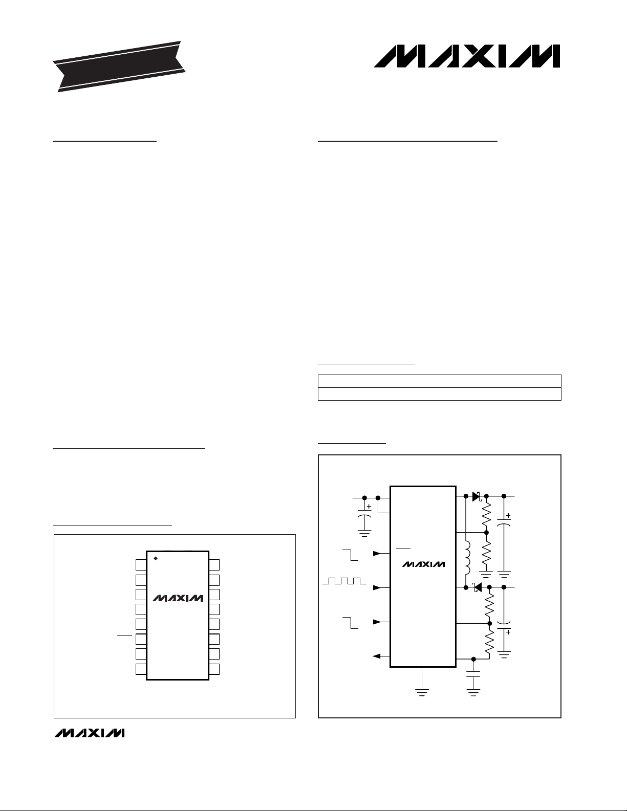
Pin Configuration
Ordering Information
TOP VIEW
16
15
I.C.
14
PGND
13
PGND
12
FBP
REF
11
10
FBN
9
GND
1
LXP LXN
I.C.
2
I.C. = INTERNALLY CONNECTED
VP
3
4
POK
SEQ
5
SHDN
6
7
SYNC
V
8
DD
MAX685
QSOP
Page 2
MAX685
Dual-Output (Positive and Negative),
DC-DC Converter for CCD and LCD
2 _______________________________________________________________________________________
ABSOLUTE MAXIMUM RATINGS
ELECTRICAL CHARACTERISTICS
(VDD= VP = 5V, TA= 0°C to +85°C unless otherwise noted. Typical values are at TA= +25°C.)
Stresses beyond those listed under “Absolute Maximum Ratings” may cause permanent damage to the device. These are stress ratings only, and functional
operation of the device at these or any other conditions beyond those indicated in the operational sections of the specifications is not implied. Exposure to
absolute maximum rating conditions for extended periods may affect device reliability.
VDD, VP to GND........................................................-0.3V to +6V
PGND to GND .......................................................-0.3V to +0.3V
V
DD
to VP...............................................................-0.3V to +0.3V
LXN, POK to GND ..................................................-0.3V to +30V
LXP to V
DD
..............................................................-15V to +0.3V
REF, SEQ,
SHDN to GND...........................-0.3V to (VDD+ 0.3V)
FBP, FBN, SYNC to GND .........................................-0.3V to +6V
Continuous Power Dissipation (T
A
= +70°C)
16-Pin QSOP (derate 8.3mW/°C above +70°C)............667mW
Operating Temperature Range ...........................-40°C to +85°C
Junction Temperature......................................................+150°C
Storage Temperature Range.............................-65°C to +165°C
Lead Temperature (soldering, 10sec).............................+300°C
2.7V < VDD< 5.5V
2.7V < VDD< 5.5V
VDD= 5.5V (Note 1)
No load
VDD= VP
No load
C3 = C4 = 10µF, I
LOAD
= 5mA
I
OUT
= 0 to 10mA, C1 = 10µF
VDD= rising
VDD= 4.5V to 5.5V
V
FBP
= 1.35V, V
FBN
= -0.1V
VDD= 4.5V, V
OUT+
≥ 14.25V, V
OUT-
≤ -7.125V,
Figure 3
TA= +25°C
VDD= 4.5V
SYNC = SEQ = SHDN = GND
SYNC = V
DD
CONDITIONS
µA0.1 1Input Bias Current
V0.7 x V
DD
Logic-High Input
V0.3 x V
DD
Logic-Low Input
µA±0.01 ±0.1FBP, FBN Input Leakage Current
mV-16 10 36FBN Threshold Voltage
V1.21 1.24 1.27FBP Threshold Voltage
mV50UVLO Hysteresis
V2.35 2.5 2.65UVLO Threshold
µA0.1 10Shutdown Supply Current
V-9 -1.27Negative Output Voltage Range
VVP 24
V2.7 5.5Input Voltage Range
Positive Output Voltage Range
mVp-p30Output Voltage Ripple
%/mA0.13Load Regulation
%/V0.2Line Regulation
µA300 500Idle Quiescent Current
mA10Output Current
mA440LX Current Limit
Ω0.6 2LXP, LXN On-Resistance
mA0.8Quiescent Current
UNITSMIN TYP MAXPARAMETER
0 < I
REF
< 50µA
No load
mV-2V
REF
Load Regulation
V1.23 1.250 1.27V
REF
Output Voltage
SHUTDOWN (SHDN)
UNDERVOLTAGE LOCKOUT
REFERENCE VOLTAGE
FB INPUTS
LOGIC INPUTS (SEQ, SHDN, SYNC)
Page 3
MAX685
Dual-Output (Positive and Negative),
DC-DC Converter for CCD and LCD
_______________________________________________________________________________________ 3
ELECTRICAL CHARACTERISTICS (continued)
(VDD= VP = 5V, TA= 0°C to +85°C unless otherwise noted. Typical values are at TA= +25°C.)
ELECTRICAL CHARACTERISTICS
(VDD, VP = 5V, TA= -40°C to +85°C unless otherwise noted.) (Note 2)
Note 1: Negative output voltage can be larger magnitude for lower values of V
DD
. The voltage between VDDand V
OUT-
must not
exceed 14.5V.
Note 2: Specifications to -40°C are guaranteed by design, not production tested.
VDD= 5.5V (Note 1)
VDD= VP
No load
VDD= rising
VIN= 4.5V, V
OUT+
≥ 14.25V, V
OUT-
≤ -7.125V,
Figure 3
SYNC = GND
SYNC = SEQ = SHDN = GND
CONDITIONS
V-9 -1.27Negative Output Voltage Range
VVP 24
V2.7 5.5Input Voltage Range
Positive Output Voltage Range
V1.205 1.275FBP Threshold Voltage
V2.35 2.65UVLO Threshold
mA10Maximum Output Current
µA500Idle Quiescent Current
µA10Shutdown Supply Current
UNITSMIN MAXPARAMETER
CONDITIONS
SYNC = V
DD
SYNC = GND
kHz
320 400 480
Oscillator Frequency (internal)
175 220 265
kHz200 480Sync Frequency Range (external)
I
POK
= 2mA
FBN falling
FBP rising
V0.4POK Output Low Voltage
mV
UNITSMIN TYP MAX
54 79 108
PARAMETER
FBN POK Threshold
V1.090 1.122 1.150FBP POK Threshold
V
POK
= 10V µA1POK Output Off Current
2.7V < VDD≤ 5.5V
No load
V0.3 x V
DD
Logic-Low Input
mV-20 40FBN Threshold Voltage
2.7V < VDD≤ 5.5V V0.7 x V
DD
Logic-High Input
FBP rising V1.090 1.150FBP POK Threshold
FBN falling mV54 108FBN POK Threshold
SYNC INPUT
POK COMPARATORS
No load V1.225 1.275VREF Output Voltage
SHUTDOWN
UNDERVOLTAGE LOCKOUT
FB INPUTS AND REFERENCE VOLTAGE
LOGIC INPUTS (SEQ, SHDN, SYNC)
POK COMPARATORS
Page 4
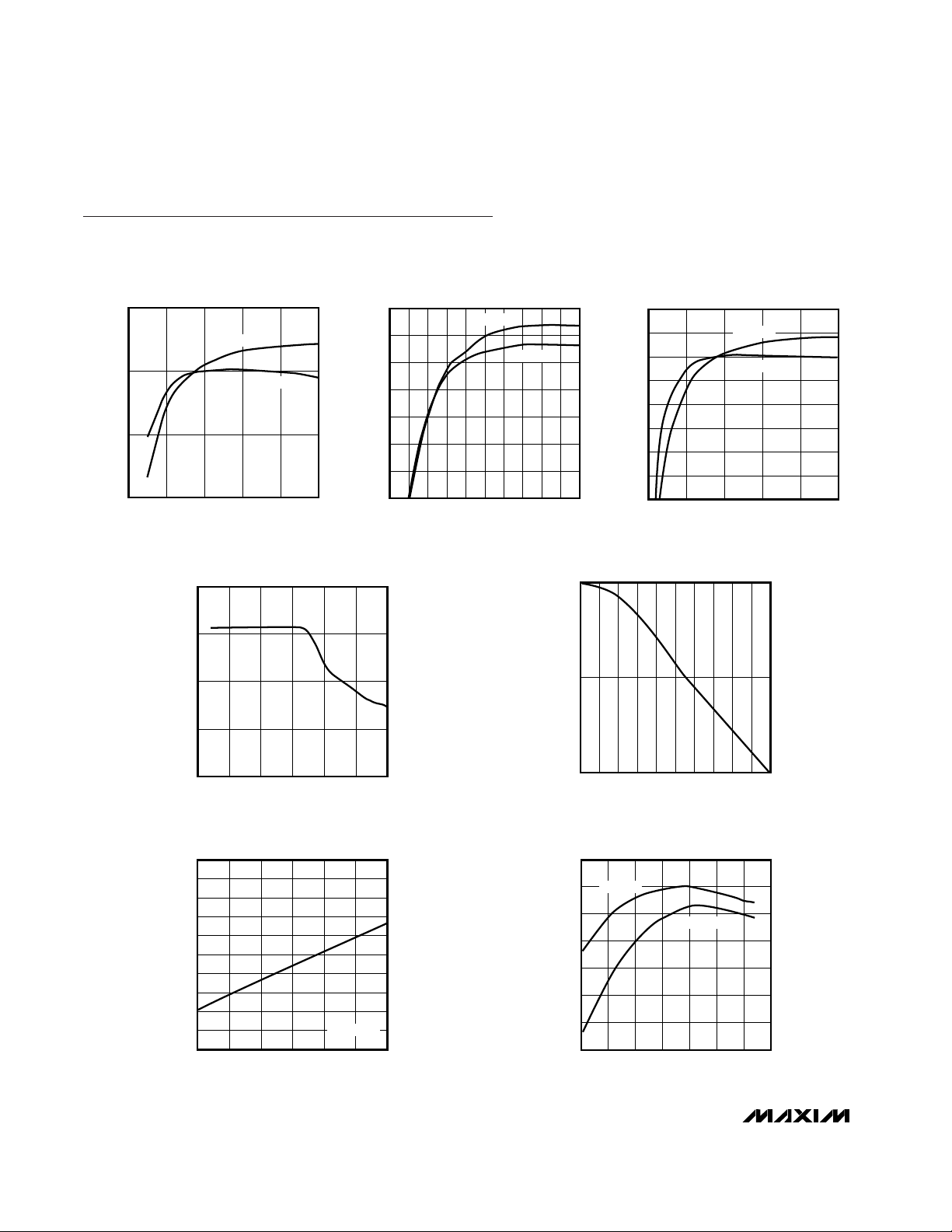
1.240
1.242
1.244
1.248
1.246
1.250
1.252
1.254
-40 200-20 40 60 80 100
REFERENCE VOLTAGE
vs. TEMPERATURE
MAX685-13
TEMPERATURE (°C)
REFERENCE VOLTAGE (V)
VIN = 5.0V
VIN = 3.3V
MAX685
Dual-Output (Positive and Negative),
DC-DC Converter for CCD and LCD
4 _______________________________________________________________________________________
60
70
80
90
0 42 6 8 10
EFFICIENCY vs. LOAD CURRENT
(POSITIVE OUTPUT LOADED)
MAX685-01
LOAD CURRENT (mA)
EFFICIENCY (%)
VIN = 5.0V
VIN = 3.3V
50
60
55
70
65
80
75
85
0 42 3 51 6 7 98 10
EFFICIENCY vs. LOAD CURRENT
(NEGATIVE OUTPUT LOADED)
MAX685-02
LOAD CURRENT (mA)
EFFICIENCY (%)
VIN = 5.0V
VIN = 3.3V
50
65
55
60
75
70
85
80
90
0 42 6 8 10
EFFICIENCY vs. LOAD CURRENT
(BOTH OUTPUTS LOADED)
MAX685-03
LOAD CURRENT (mA)
EFFICIENCY (%)
VIN = 5.0V
VIN = 3.3V
0
0.5
1.0
1.5
2.0
2.5 3.53.0 4.0 4.5 5.0 5.5
NO-LOAD CURRENT vs.
INPUT VOLTAGE
MAX685-04
INPUT VOLTAGE (V)
NO-LOAD CURRENT (mA)
150
180
170
160
190
200
210
220
230
240
250
2.7 3.73.2 4.2 4.7 5.2 5.7
LX SWITCHING FREQUENCY
vs. INPUT VOLTAGE
MAX865-07
INPUT VOLTAGE (V)
OSCILLATOR FREQUENCY (kHz)
SYNC = V
DD
1.248
1.249
1.250
0 15 205 10 25 30 35 40 45 50
REFERENCE LOAD REGULATION
MAX685-06
LOAD CURRENT (µA)
REFERENCE VOLTAGE (V)
Typical Operating Characteristics
(Circuit of Figure 3, V
OUT+
= 15V, V
OUT-
= -7.5V, TA= +25°C, unless otherwise noted.)
Page 5

MAX685
Dual-Output (Positive and Negative),
DC-DC Converter for CCD and LCD
_______________________________________________________________________________________
5
11mA
5mA/div
100mV/div
1mA
I
OUT+
V
OUT+
2ms/div
V
OUT+
LOAD-TRANSIENT RESPONSE
MAX685-08
-1mA
5mA/div
100mV/div
-11mA
I
OUT-
V
OUT-
2ms/div
V
OUT-
LOAD-TRANSIENT RESPONSE
MAX685-09
100mV/div
V
OUT+
V
OUT-
VDD, VP
2V/div
100mV/div
1ms/div
INPUT 4V TO 5V, +15V AT 10mA, -7.5V AT 10mA
LINE-TRANSIENT RESPONSE
MAX685-10
5V/div
V
OUT+
V
OUT-
5V/div
2ms/div
START-UP, SEQ = LOW, V
DD
= VP = 5.0V,
+15V AT 10mA, -7.5V AT 10mA
START-UP (SEQ = LOW)
MAX685-11
5V/div
V
OUT+
V
OUT-
5V/div
2ms/div
START-UP, SEQ = HIGH, V
DD
= VP = 5.0V,
+15V AT 10mA, -7.5V AT 10mA
START-UP (SEQ = HIGH)
MAX685-12
Typical Operating Characteristics (continued)
(Circuit of Figure 3, V
OUT+
= 15V, V
OUT-
= -7.5V, TA= +25°C, unless otherwise noted.)
Page 6

_______________Detailed Description
The MAX685 DC-DC converter accepts an input voltage
between +2.7V and +5.5V and generates both a positive
and negative voltage, using a single inductor (Figure 1).
It alternates between acting as a step-up converter and
as an inverting converter on a cycle-by-cycle basis. Both
output voltages are independently regulated.
Each output is separately controlled by a pulse-widthmodulated (PWM) current mode regulator. This allows
the part to operate at a fixed frequency for use in noisesensitive applications. An internal oscillator runs at
220kHz or 400kHz, or can be synchronized to an external signal. Since switching alternates between the two
regulators, each operates at half the oscillator frequency
(110kHz, 200kHz, or half the sync frequency). The oscillator can be synchronized to a 200kHz to 480kHz clock.
On the first cycle of operation, the part operates as a
step-up converter. LXP connects to VDD, LXN pulls to
ground, and the inductor current rises. Once the induc-
tor current rises to a level set by the positive-side error
amplifier, LXN releases and the inductor current flows
through D2 to the positive output. When the inductor
current drops to zero (which happens each cycle under
normal, discontinuous operation), LXN returns to the
input voltage.
On the second cycle, LXN is held at ground. LXP is
pulled up to the input voltage until the current reaches
the limit set by the negative error amplifier. Then LXP is
released and the inductor current flows through D1 to
the negative output. Once the inductor current reaches
zero, the voltage at LXP returns to ground. The waveforms at LXN and LXP are shown in Figure 2 for a typical pair of cycles.
The current into the LXN pin is sensed to measure the
inductor current. The MAX685 controls the inductor current to regulate both the positive and negative output
voltages.
MAX685
Dual-Output (Positive and Negative),
DC-DC Converter for CCD and LCD
6 _______________________________________________________________________________________
Pin Description
PIN
P-Channel Switching Inductor Node. LXP turns off when the part enters shutdown.LXP1
FUNCTIONNAME
Internally Connected. Do not externally connect.I.C.2, 15
Open-Drain Power-OK Output. POK is high when both outputs are in regulation. Connect POK to VDDwith a
100kΩ pull-up resistor to VDD.
POK4
Power Input. Connect to VDD.VP3
Shutdown Input. Both outputs go to 0V in shutdown. Connect to VDDfor automatic startup.
SHDN
6
Supply Input. Bypass VDDwith a 1.0µF or greater ceramic capacitor to GND.V
DD
8
Sync Input. This pin synchronizes the oscillator to an external clock frequency between 200kHz and 480kHz.
Connect SYNC to GND (220kHz) or VDD(400kHz) for internal oscillator frequency.
SYNC7
Power-Up Sequence Select Input. Connect SEQ to GND to power the negative output voltage first. Connect
SEQ to VDDto power the positive output first.
SEQ5
GroundGND9
1.25V Reference Voltage Output. Bypass with 0.22µF to GND.REF11
Power Ground. Connect PGND to GND.PGND13, 14
Feedback for the Positive Output Voltage. Connect a resistor-divider between the positive output and GND
with the center to FBP to set the positive output voltage.
FBP12
Feedback Input for the Negative Output Voltage. Connect a resistor-divider between the negative output
and REF with the center to FBN to set the negative output voltage.
FBN10
N-Channel Switching Inductor Node. LXN pulls to GND through the internal transistor when the part is shut
down.
LXN16
Page 7

SEQ and Power OK (POK)
The SEQ pin controls the power-up sequence. If SEQ is
low, the positive output is disabled until the negative
output is within 90% of its regulation point. If SEQ is
high, the negative output is disabled until the positive
output is within 90% of its regulation point. The powerOK output (POK) indicates that both output voltages
are in regulation. When both outputs are within 90% of
their regulation points, POK becomes high impedance.
Should one or both of the output voltages fall below
90% of their regulation points, POK pulls to ground.
POK can sink up to 2mA. To reduce current consumption, POK is high impedance while the part is in shutdown. When coming out of shutdown, POK remains
high impedance for 50ns (typ) before going low.
Connect POK to V
DD
through a 100kΩ resistor.
Synchronization/Internal
Frequency Selection
The MAX685 operates at a fixed switching frequency.
Set the operating frequency using the SYNC pin. If
SYNC is grounded, the part operates at the internally set
220kHz frequency. When SYNC is connected to VDD,
the part operates at 400kHz. The MAX685 can also be
synchronized to signals between 200kHz and 480kHz.
Note that each output switches at half the oscillator or
synchronized frequency. Since the actual switching frequency is one-half the applied clock signal, drive SYNC
at twice the desired switching frequency.
MAX685
Dual-Output (Positive and Negative),
DC-DC Converter for CCD and LCD
_______________________________________________________________________________________ 7
Figure 1. Functional Diagram
NEGATIVE
ERROR
AMP
TO V
OUT-
FBN
FBP
TO V
OUT+
REF
POSITIVE
ERROR
AMP
1.25V
REF
CONTROL
LOGIC
POK VP
V
DD
P
N
PGND
GND
SYNC SEQ SHDN
LXN
D2
D1
V
OUT-
V
OUT+
LXP
MAX685
Figure 2. LXN and LXP Waveforms (see also Figure 5)
LXN
LXP
+15V
0V
+5V
0V
-7.5V
Page 8

MAX685
Applications Information
Figure 3 shows the standard application circuit for the
MAX685. The values shown in Table 1 will work well for
output currents up to 10mA. However, this circuit can
be optimized to a particular application by using different capacitors and a different inductor.
Higher Output Voltages
If the application requires output voltages greater than
-7.5V or +24V, use the circuit of Figure 4. This circuit
uses a charge pump to increase the output voltage
without increasing the voltage stress on the LX_ pin.
The maximum output voltages of the circuit in Figure 4
are -15V and +48V.
The voltage rating on D2, D5, and D6 must be 30V or
greater. For a larger negative output voltage without a
larger positive output (or vice versa), use one-half of
the Figure 4 circuit with one-half of the Figure 3 circuit.
Inductor Selection
A 22µH inductor is suitable for most applications.
Larger inductances will reduce inductor ripple current
and output voltage ripple, but they also typically require
larger physical size if increased resistance and losses
are not also allowed.
Small inductors are typically preferred because of
compact design and low cost. Murata LHQ and
TDK NLC types are examples of small surface-mount
inductors that work for most applications. Because these
small-size inductors use thinner wire, they exhibit higher
resistance and have greater losses than larger ones. If
the application demands higher efficiency, use larger,
lower resistance coils such as the Sumida CD43 or CD54,
Coilcraft DT1608 or DO1608, or Coiltronics UP1V series.
Filter Capacitor Selection
The output ripple voltage is a function of the peak inductor current, frequency, and type and value of the
output capacitors. Capacitors with low equivalentseries resistance (ESR) and large capacitance reduce
output ripple. Typically, tantalum or ceramic capacitors
are optimal. Tantalum capacitors have higher ESR and
higher capacitance than ceramic capacitors. Therefore
the ESR of tantalum capacitors determines the output
ripple, because at the frequencies used the ESR dominates the impedance of the capacitor. If ceramic
capacitors are used, the capacitance determines the
output ripple.
Dual-Output (Positive and Negative),
DC-DC Converter for CCD and LCD
8 _______________________________________________________________________________________
MAX685
REF
VP V
DD
LXP
1
11
3 8
9 13, 14 16
FBN
10
POK
4
6
7
12
POK
SHDN
SYNC
C5
47pF
R1
1.0M
R5
100k
D2
NBR0520
L1
22µH
D1
NBR0520
R2
90.9k
+15V
V
OUT+
C4
2.2µF
C3
2.2µF
C2
0.22µF
C1
10µF
V
IN
R3
750k
R4
124k
-7.5V
V
OUT-
SHDN
PGND
LXNGND
SYNC
FBP
Figure 3. Standard Application Circuit
MAX685
REF
VP V
DD
LXP
C6
1µF
1
11
3 8
9 13, 14 16
C8
1µF
FBN
10
POK
4
6
7
12
POK
SHDN
SYNC
C5
47pF
R1
R5
100k
D2
D5
D6
L1
22µH
D3
D4 D1
R2
V
OUT+
C9
2.2µF
C7
2.2µF
C3
2.2µF
C2
0.22µF
C1
10µF
V
IN
R3
R4
V
OUT-
SHDN
PGND
LXNGND
SYNC
FBP
C4
2.2µF
Figure 4. Circuit for Output Voltages < -9V and > +24V
Page 9

Setting the Output Voltage
The resistor-divider formed by R4 and R3 sets the negative output voltage; the resistor-divider formed by R1
and R2 sets the positive output voltage. Let R4 be a
value near 100kΩ to set a resistor-divider current of
approximately 10µA. Determine the value of R3 by the
following:
Let R2 be a value near 100kΩ to set a resistor-divider
current of approximately 10µA. Determine the value of
R1 with the following formula:
R1 = R2 x (V
OUT
+ - 1.24V) / 1.24
Damping LX
LXN and LXP may ring at the conclusion of each
switching cycle when the inductor current falls to zero.
Typically the ringing waveform appears only on LX_
and has no effect on output ripple and noise. If LX_
ringing is still objectionable, it may be damped by connecting a series RC in parallel with L1. Typically 1kΩ in
series with 100pF provides good damping with only 3%
efficiency degradation. See Figure 5.
R R
V
V
OUT
3 4
1 24
.
=
−
MAX685
Dual-Output (Positive and Negative),
DC-DC Converter for CCD and LCD
_______________________________________________________________________________________ 9
Any manufacturer
0.22µF ceramic
capacitor
C2
Any manufacturer47pF ceramic capC5
Any manufacturer
2.2µF ceramic
capacitor
C3, C4
Murata LHQ4N220J04 or
TDK NLC32522T-220K
22µH, 0.4A
inductor
L1
Motorola MBR0520LT1 (0.5A)
or Central Semiconductor
CMPSH-3
0.1A, 20V
Schottky rectifier
D1, D2
REF
Sprague 595D106X0010A2T or
AVX TAJA106K010R
10µF, 10V
tantalum cap
C1
MANUFACTURER
PART NUMBER
DESCRIPTION
Table 1. Component Values for the
Typical Operating Circuit
Figure 5. LXN and LXP Waveforms with a Series-Connected
1k
Ω
Resistor and 100pF Capacitor Connected in Parallel with
L1 to Damp Ringing
+15V
+5V
0V
+5V
0V
-7.5V
LXN
LXP
Page 10

MAX685
Dual-Output (Positive and Negative),
DC-DC Converter for CCD and LCD
10 ______________________________________________________________________________________
Package Information
QSOP.EPS
___________________Chip Information
TRANSISTOR COUNT: 902
SUBSTRATE CONNECTED TO GND
Page 11

MAX685
Dual-Output (Positive and Negative),
DC-DC Converter for CCD and LCD
______________________________________________________________________________________ 11
NOTES
Page 12

MAX685
Dual-Output (Positive and Negative),
DC-DC Converter for CCD and LCD
NOTES
12 ______________________________________________________________________________________
 Loading...