

Page 1
19-0896; Rev 1; 7/96
+5V to ±10V Voltage Converters
________________General Description
The MAX680/MAX681 are monolithic, CMOS, dual
charge-pump voltage converters that provide ±10V outputs from a +5V input voltage. The MAX680/MAX681 provide both a positive step-up charge pump to develop
+10V from +5V input and an inverting charge pump to
generate the -10V output. Both parts have an on-chip,
8kHz oscillator. The MAX681 has the capacitors internal to
the package, and the MAX680 requires four external
capacitors to produce both positive and negative voltages
from a single supply.
The output source impedances are typically 150Ω, providing useful output currents up to 10mA. The low quiescent current and high efficiency make this device suitable
for a variety of applications that need both positive and
negative voltages generated from a single supply.
The MAX864/MAX865 are also recommended for new
designs. The MAX864 operates at up to 200kHz and uses
smaller capacitors. The MAX865 comes in the smaller
µMAX package.
________________________Applications
The MAX680/MAX681 can be used wherever a single
positive supply is available and where positive and negative voltages are required. Common applications include
generating ±6V from a 3V battery and generating ±10V
from the standard +5V logic supply (for use with analog
circuitry). Typical applications include:
±6V from 3V Lithium Cell
Hand-Held Instruments
Data-Acquisition Systems
Panel Meters
Battery-Operated
Equipment
Operational Amplifier
Power Supplies
±10V from +5V Logic
Supply
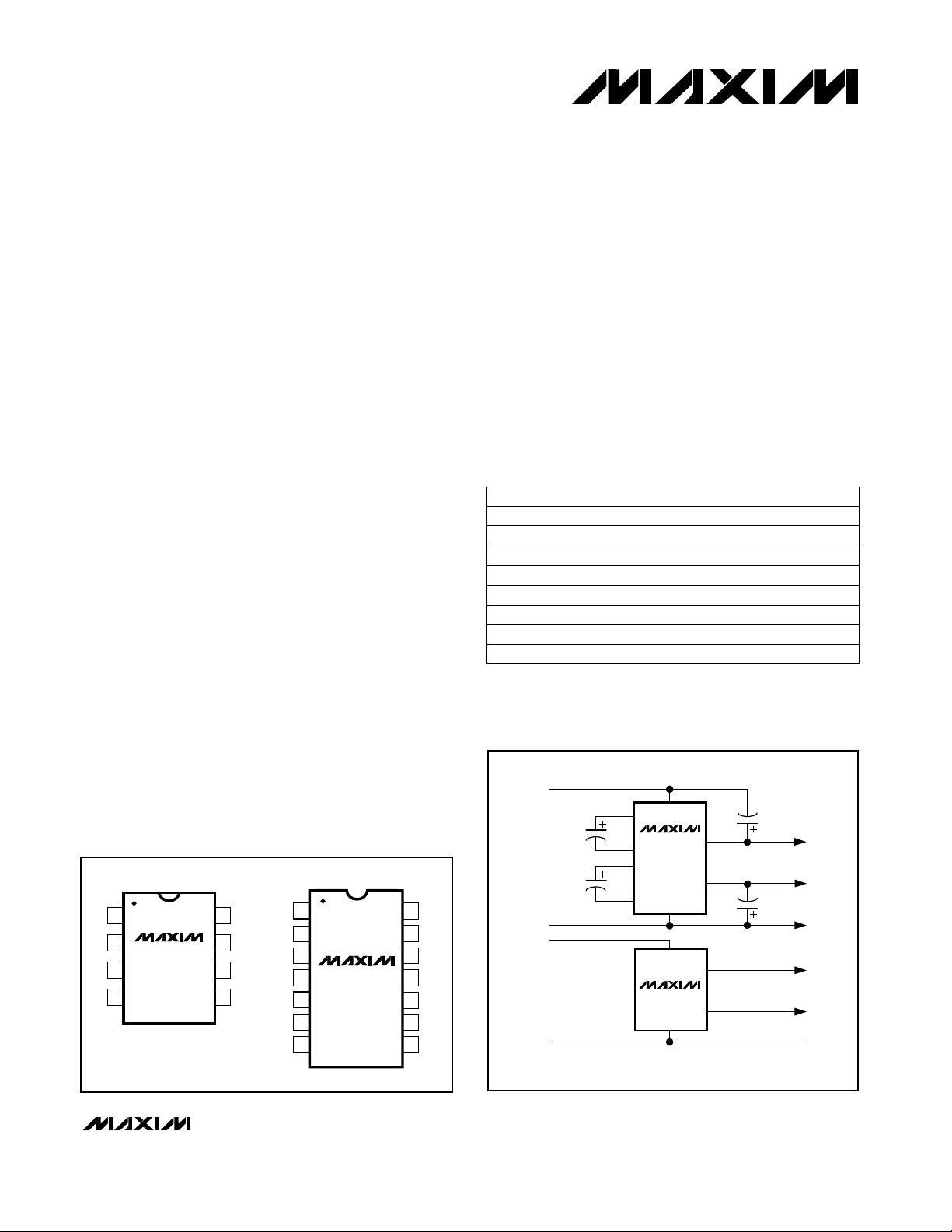
_________________Pin Configurations
TOP VIEW
C1-
C2+
C2-
V+
C1C1-
C2+
C2C2-
1
2
3
MAX681
4
5
6
V-
7
DIP
1
2
MAX680
3
4
V-
DIP/SO
8
V+
C1+
7
V
6
CC
GND
5
V
CC
14
V
CC
13
V
CC
12
V
11
CC
V+
10
GND
9
GND
8
____________________________Features
♦ 95% Voltage-Conversion Efficiency
♦ 85% Power-Conversion Efficiency
♦ +2V to +6V Voltage Range
♦ Only Four External Capacitors Required (MAX680)
♦ No Capacitors Required (MAX681)
♦ 500µA Supply Current
♦ Monolithic CMOS Design
_______________Ordering Information
PART
MAX680CPA
MAX680CSA
MAX680C/D 0°C to +70°C
MAX680EPA
MAX680ESA -40°C to +85°C
MAX680MJA -55°C to +125°C 8 CERDIP
MAX681CPD
MAX681EPD -40°C to +85°C
TEMP. RANGE PIN-PACKAGE
0°C to +70°C
0°C to +70°C
8 Plastic DIP
8 Narrow SO
Dice
-40°C to +85°C 8 Plastic DIP
8 Narrow SO
0°C to +70°C 14 Plastic DIP
14 Plastic DIP
_________Typical Operating Circuits
+5V
V
4.7µF
4.7µF
GND
+5V
FOUR PINS REQUIRED
(MAX681 ONLY)
GND
CC
C1+
MAX680
GND
V
CC
MAX681
GND
V+
V-
V+
V-
C1C1+
C2-
+5V to ±10V CONVERTER
4.7µF
+10V
-10V
4.7µF
GND
+10V
-10V
GND
MAX680/MAX681
________________________________________________________________
Maxim Integrated Products
1
For free samples & the latest literature: http://www.maxim-ic.com, or phone 1-800-998-8800
Page 2
+5V to ±10V Voltage Converters
ABSOLUTE MAXIMUM RATINGS
VCC................................................................................... +6.2V
V+ ...................................................................................... +12V
V- ..........................................................................................-12V
V- Short-Circuit Duration ...........................................Continuous
V+ Current ..........................................................................75mA
∆V/∆T ..........................................................................1V/µs
V
CC
Stresses beyond those listed under “Absolute Maximum Ratings” may cause permanent damage to the device. These are stress ratings only, and functional
operation of the device at these or any other conditions beyond those indicated in the operational sections of the specifications is not implied. Exposure to
absolute maximum rating conditions for extended periods may affect device reliability.
Continuous Power Dissipation (T
8-Pin Plastic DIP (derate 9.09mW/°C above +70°C) .....727mW
8-Pin Narrow SO (derate 5.88mW/°C above +70°C) .....471mW
8-Pin CERDIP (derate 8.00mW/°C above +70°C) ..........640mW
14-Pin Plastic DIP (derate 10.00mW/°C above +70°C) ...800mW
Storage Temperature Range .............................-65°C to +160°C
Lead Temperature (soldering, 10sec) .............................+300°C
ELECTRICAL CHARACTERISTICS
(VCC= +5V, test circuit Figure 1, TA= +25°C, unless otherwise noted.)
CONDITIONS UNITSPARAMETER
MIN TYP MAX
= +70°C)
A
MAX680/MAX681
Supply Current mA
Positive Charge-Pump
Output Source Resistance
Negative Charge-Pump
Output Source Resistance
Voltage-Conversion
Efficiency
VCC= 3V, TA= +25°C, RL= ∞
VCC= 5V, TA= +25°C, RL= ∞
VCC= 5V, 0°C ≤ TA≤ +70°C, RL= ∞
VCC= 5V, -40°C ≤ TA≤ +85°C, RL= ∞
VCC= 5V, -55°C ≤ TA≤ +125°C, RL= ∞
MIN ≤ TA≤ MAX, RL= 10kΩ
IL+ = 10mA, IL- = 0mA, VCC= 5V,
TA= +25°C
IL+ = 5mA, IL- = 0mA, VCC= 2.8V,
TA= +25°C
IL+ = 10mA,
IL- = 0mA,
VCC= 5V
IL- = 10mA, IL+ = 0mA, V+ = 10V,
TA= +25°C
IL- = 5mA, IL+ = 0mA, V+ = 5.6V,
TA= +25°C
IL- = 10mA,
IL+ = 0mA,
V+ = 10V
RL= 10kΩ
V+, RL= ∞
V-, RL= ∞
0°C ≤ TA≤ +70°C
-40°C ≤ TA≤ +85°C
-55°C ≤ TA≤ +125°C
0°C ≤ TA≤ +70°C
-40°C ≤ TA≤ +85°C
-55°C ≤ TA≤ +125°C
0.5 1
12
2.5
3
3
2.0 1.5 to 6.0 6.0Supply-Voltage Range
150 250
180 300
325
350
400
90 150
110 175
200
200
250
48Oscillator Frequency
95 99
90 97
V
Ω
Ω
kHz
%85Power Efficiency
%
2 _______________________________________________________________________________________
Page 3
+5V to ±10V Voltage Converters
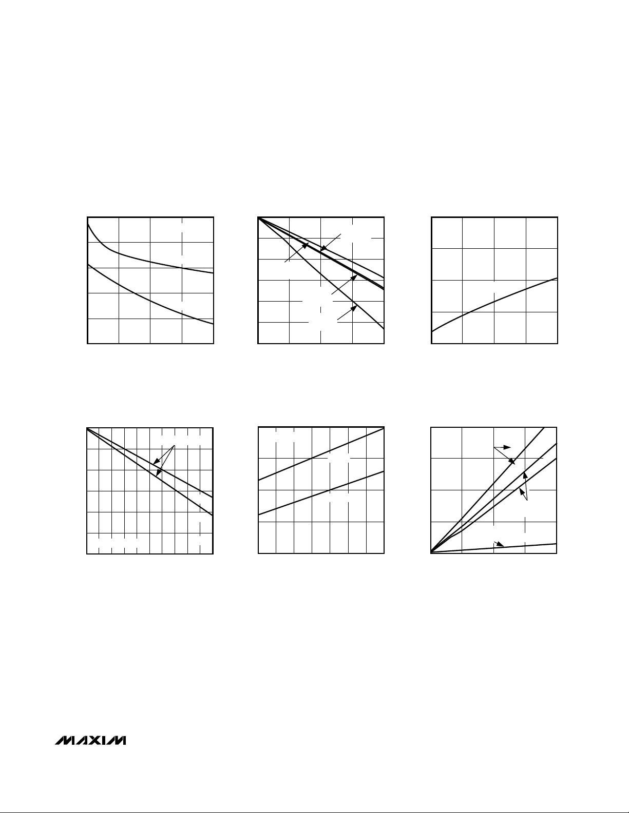
__________________________________________Typical Operating Characteristics
(TA = +25°C, unless otherwise noted.)
OUTPUT RESISTANCE
vs. SUPPLY VOLTAGE
250
C1-C4 = 10µF
200
150
100
OUTPUT RESISTANCE (Ω)
50
0
2.0
3.0
4.0
OUTPUT VOLTAGE vs. OUTPUT CURRENT
(FROM V+ TO V-)
10
9
8
(V)
|
7
VOUT
|
6
5
C1–C4 = 10µF
4
01234 6789
OUTPUT CURRENT (mA)
MAX680, MAX681
510
R
5.0
R
OUT
OUT
10
9
MAX680/681-TOC1
+
-
6.0
MAX680/681-TOC4
V+
V-
(V)
|
VOUT
|
200
150
100
50
OUTPUT SOURCE RESISTANCE (Ω)
8
7
6
5
4
0
0
-50
OUTPUT VOLTAGE
vs. LOAD CURRENT
V- vs. IL+
- = 0
I
L
V+ vs. IL+
- = 0
I
L
V+ vs. IL-
+ = 0
I
L
V- vs. IL-
+ = 0
I
L
5
10
15
OUTPUT SOURCE RESISTANCE
vs. TEMPERATURE
VCC = 5V
R
+
OUT
R
-
OUT
-25 0 25 50 75 100
TEMPERATURE (°C)
MAX680/681-TOC2
SUPPLY CURRENT (mA)
20
MAX680/681-TOC5
100
OUTPUT RIPPLE (mVp-p)
125
200
150
2.0
1.5
1.0
0.5
0
2.0
OUTPUT CURRENT (I
VCC = 5V
50
0
0
SUPPLY CURRENT
vs. SUPPLY VOLTAGE
RL = ∞
3.0
4.0
OUTPUT RIPPLE vs.
+ OR I
L
MAX681
MAX680
C3, C4 = 100µF
5
OUTPUT CURRENT (mA)
V-
V+
C3, C4 = 10µF
10
5.0
MAX680
V+ AND V-
15
6.0
-)
L
V-
V+
20
MAX680/MAX681
MAX680/681-TOC3
MAX681/681-TOC6
_______________________________________________________________________________________
3
Page 4

+5V to ±10V Voltage Converters
_______________Detailed Description
The MAX681 contains all circuitry needed to implement
a dual charge pump. The MAX680 needs only four
IN
V
CC
C1
4.7µF
C2
4.7µF
MAX680
1
C1-
2
C2+
3
C2-
4
V-
C1+
V
GND
8
V+
7
6
CC
5
C3
10µF
MAX680/MAX681
C4
10µF
Figure 1. Test Circuit
IL+
I
V+ OUT
+
R
L
-
L
GND
-
R
L
V- OUT
capacitors. These may be inexpensive electrolytic
capacitors with values in the 1µF to 100µF range. The
MAX681 contains two 1.5µF capacitors as C1 and C2,
and two 2.2µF capacitors as C3 and C4. See
Operating Characteristics.
Figure 2a shows the idealized operation of the positive
voltage converter. The on-chip oscillator generates a
50% duty-cycle clock signal. During the first half of the
cycle, switches S2 and S4 are open, S1 and S3 are
closed, and capacitor C1 is charged to the input voltage VCC. During the second half-cycle, S1 and S3 are
open, S2 and S4 are closed, and C1 is translated
upward by VCCvolts. Assuming ideal switches and no
load on C3, charge is transferred onto C3 from C1 such
that the voltage on C3 will be 2VCC, generating the
positive supply.
Figure 2b shows the negative converter. The switches
of the negative converter are out of phase from the positive converter. During the second half of the clock
cycle, S6 and S8 are open and S5 and S7 are closed,
charging C2 from V+ (pumped up to 2VCCby the positive charge pump) to GND. In the first half of the clock
Typical
a) b)
V+
CC
V
GND
CC
S1
S3
8kHz
C1+
S2
C1
C1-
C3
S4
Figure 2. Idealized Voltage Quadrupler: a) Positive Charge Pump; b) Negative Charge Pump
4 _______________________________________________________________________________________
V+
IL+
GNDV
S5
RL+
S7 S8
C2
C2+
C2-
S6
C4
GND
R
-
IL-
L
V-
Page 5

+5V to ±10V Voltage Converters
cycle, S5 and S7 are open, S6 and S8 are closed, and
the charge on C2 is transferred to C4, generating the
negative supply. The eight switches are CMOS power
MOSFETs. S1, S2, S4, and S5 are P-channel
switches, while S3, S6, S7, and S8 are N-channel
switches.
__________Efficiency Considerations
Theoretically, a charge-pump voltage multiplier can
approach 100% efficiency under the following conditions:
• The charge-pump switches have virtually no offset
and extremely low on-resistance
• Minimal power is consumed by the drive circuitry
• The impedances of the reservoir and pump capacitors are negligible
For the MAX680/MAX681, the energy loss per clock
cycle is the sum of the energy loss in the positive and
negative converters as below:
LOSS
TOT
= LOSS
POS
+ LOSS
=1⁄2C1[(V+)2– (V+)(VCC)
1
⁄2C2[(V+)2– (V-)
NEG
2
] +
]
There will be a substantial voltage difference between
(V+ - VCC) and VCCfor the positive pump, and
between V+ and V-, if the impedances of pump capacitors C1 and C2 are high relative to their respective output loads.
Larger C3 and C4 reservoir capacitor values reduce
output ripple. Larger values of both pump and reservoir
capacitors improve efficiency.
________Maximum Operating Limits
The MAX680/MAX681 have on-chip zener diodes that
clamp VCCto approximately 6.2V, V+ to 12.4V, and
V- to -12.4V. Never exceed the maximum supply voltage: excessive current may be shunted by these
diodes, potentially damaging the chip. The MAX680/
MAX681 operate over the entire operating temperature
range with an input voltage of +2V to +6V.
________________________Applications
Positive and Negative Converter
The most common application of the MAX680/MAX681
is as a dual charge-pump voltage converter that provides positive and negative outputs of two times a positive input voltage. For applications where PC board
space is at a premium, the MAX681, with its capacitors
internal to the package, offers the smallest footprint.
The simple circuit shown in Figure 3 performs the same
function using the MAX680 with external capacitors C1
and C3 for the positive pump and C2 and C4 for the
negative pump. In most applications, all four capacitors
are low-cost, 10µF or 22µF polarized electrolytics.
When using the MAX680 for low-current applications,
1µF can be used for C1 and C2 charge-pump capacitors, and 4.7µF for C3 and C4 reservoir capacitors.
C1 and C3 must be rated at 6V or greater, and C2 and
C4 must be rated at 12V or greater.
C1
22µF
C2
22µF
MAX680
1
C1-
2
C2+
3
C2-
4
V-
C1+
V
GND
8
V+
7
6
CC
5
C3
22µF
C4
22µF
V+ OUT
IN
V
CC
GND
V- OUT
MAX680/MAX681
Figure 3. Positive and Negative Converter
_______________________________________________________________________________________ 5
Page 6

+5V to ±10V Voltage Converters
22µF
MAX680
1
C1-
2
C2+
22µF
MAX680/MAX681
Figure 4. Paralleling MAX680s For Lower Source Resistance
3
C2-
4
V-
C1+
V
GND
8
V+
7
6
CC
5
The MAX680/MAX681 are not voltage regulators: the
output source resistance of either charge pump is
approximately 150Ω at room temperature with VCCat
5V. Under light load with an input VCCof 5V, V+ will
approach +10V and V- will be at -10V. However both,
V+ and V- will droop toward GND as the current drawn
from either V+ or V- increases, since the negative converter draws its power from the positive converter’s output. To predict output voltages, treat the chips as two
separate converters and analyze them separately. First,
the droop of the negative supply (V
current drawn from V- - (I
-
) times the source resistance
L
DROP
) equals the
-
of the negative converter (RS-):
V
Likewise, the positive supply droop (V
the current drawn from the positive supply (I
DROP
-= IL- x RS-
DROP
+
L
the positive converter’s source resistance (RS+),
except that the current drawn from the positive supply
is the sum of the current drawn by the load on the posi-
(V
+
) plus the current drawn by the negative
L
-
):
L
+) = IL+ x RS+ = (IL+ + IL-) x RS+
DROP
tive supply (I
converter (I
) equals
+
) times
22µF
22µF
MAX680
1
C1-
2
C2+
3
C2-
4
V-
C1+
V
GND
8
V+
7
6
CC
5
22µF
22µF
V+ OUT
V
GND
V- OUT
The positive output voltage will be:
V+ = 2V
CC
– V
DROP
+
The negative output voltage will be:
V- = (V+ - V
DROP
) = - (2V
CC
- V
DROP
The positive and negative charge pumps are tested
and specified separately to provide the separate values
of output source resistance for use in the above formulas. When the positive charge pump is tested, the negative charge pump is unloaded. When the negative
charge pump is tested, the positive supply V+ is from
an external source, isolating the negative charge
pump.
Calculate the ripple voltage on either output by noting
that the current drawn from the output is supplied by
the reservoir capacitor alone during one half-cycle of
the clock. This results in a ripple of:
V
RIPPLE
For the nominal f
= 1⁄2IOUT (1⁄ f
of 8kHz with 10µF reservoir
PUMP
PUMP
)(1⁄ CR)
capacitors, the ripple will be 30mV with I
Remember that in most applications, the positive
charge pump’s I
is the load current plus the current
OUT
taken by the negative charge pump.
IN
CC
+ - V
OUT
DROP
at 5mA.
-)
6 _______________________________________________________________________________________
Page 7

+5V to ±10V Voltage Converters
Paralleling Devices
Paralleling multiple MAX680/MAX681s reduces the output resistance of both the positive and negative converters. The effective output resistance is the output
resistance of a single device divided by the number of
devices. As Figure 4 shows, each MAX680 requires
separate pump capacitors C1 and C2, but all can
share a single set of reservoir capacitors.
±5V Regulated Supplies from
a Single 3V Battery
Figure 5 shows a complete ±5V power supply using one
3V battery. The MAX680/MAX681 provide +6V at V+,
which is regulated to +5V by the MAX666, and -6V,
which is regulated to -5V by the MAX664. The MAX666
and MAX664 are pretrimmed at wafer sort and require
2MΩ
1.2MΩ
6V TO 3V
100µF
100µF
C1+
C1C2+
C2-
V
CC
MAX680
GND
100µF
V+
V-
100µF
no external setting resistors, minimizing part count. The
combined quiescent current of the MAX680/MAX681,
MAX663, and MAX664 is less than 500µA, while the output current capability is 5mA. The MAX680/MAX681
input can vary from 3V to 6V without affecting regulation
appreciably. With higher input voltage, more current can
be drawn from the MAX680/MAX681 outputs. With 5V at
VCC, 10mA can be drawn from both regulated outputs
simultaneously. Assuming 150Ω source resistance for
+
both converters, with (I
L
-
+ I
) = 20mA, the positive
L
charge pump will droop 3V, providing +7V for the negative charge pump. The negative charge pump will droop
another 1.5V due to its 10mA load, leaving -5.5V at Vsufficient to maintain regulation for the MAX664 at this
current.
LOW-BATTERY
WARNING AT 3.5V
LBO
+12V TO +6V
0.1µF
0.1µF
-12V TO -6V
LBI
V
IN
MAX666
SDNGND VSET
SDNGND V
MAX664
SENSE
VOUTVIN
SET
VOUT1
VOUT2
SENSE
+5V
10µF
GND
10µF
-5V
MAX680/MAX681
Figure 5. Regulated +5V and -5V from a Single Battery
_______________________________________________________________________________________ 7
Page 8

+5V to ±10V Voltage Converters
___________________Chip Topography
C1- V+
C1+
V
CC
0.116"
(2.95mm)
MAX680/MAX681
C2+
C2-
V-
0.72"
(1.83mm)
GND
________________________________________________________Package Information
DIM
D
A
0.101mm
e
A1
B
0.004in.
C
L
0°-8°
A
A1
B
C
E
H
INCHES MILLIMETERS
MIN
0.053
0.004
0.014
0.007
0.150
e
0.228
L
0.016
MAX
0.069
0.010
0.019
0.010
0.157
0.244
0.050
MIN
1.35
0.10
0.35
0.19
3.80
5.80
0.40
1.270.050
MAX
1.75
0.25
0.49
0.25
4.00
6.20
1.27
PINS
Narrow SO
HE
SMALL-OUTLINE
PACKAGE
(0.150 in.)
Maxim cannot assume responsibility for use of any circuitry other than circuitry entirely embodied in a Maxim product. No circuit patent licenses are
implied. Maxim reserves the right to change the circuitry and specifications without notice at any time.
8
___________________Maxim Integrated Products, 120 San Gabriel Drive, Sunnyvale, CA 94086 (408) 737-7600
DIM
D
D
D
INCHES MILLIMETERS
MIN
MAX
8
0.189
0.197
14
0.337
0.344
16
0.386
0.394
MIN
4.80
8.55
9.80
MAX
5.00
8.75
10.00
21-0041A
© 1989 Maxim Integrated Products Printed USA is a registered trademark of Maxim Integrated Products.
 Loading...