

Page 1
General Description
The MAX6775–MAX6781 low-power, 1%-accurate battery monitors are available in the ultra-small µDFN
package (1.0mm x 1.5mm) and SC70 packages. These
low-power devices are ideal for monitoring single lithium-ion (Li+) cells, or multicell alkaline/NiCd/NiMH
power sources. These devices offer single (MAX6775/
MAX6776/MAX6777/MAX6778) or dual (MAX6779/
MAX6780/MAX6781) low-battery outputs and feature
fixed or resistor-adjustable hysteresis. Hysteresis eliminates the output chatter sometimes associated with battery voltage monitors, usually due to input-voltage noise
or battery terminal voltage recovery after load removal.
These devices are available in several versions: with
single- or dual-voltage monitors, and with fixed or
adjustable hysteresis. The MAX6775/MAX6776 offer a
single battery monitor and factory-set hysteresis of
0.5%, 5%, or 10%. The MAX6779/MAX6780/MAX6781
have two battery monitors in a single package and factory-set hysteresis of 0.5%, 5%, or 10%. The MAX6777/
MAX6778 offer a single battery monitor with external
inputs for the rising and falling thresholds, allowing
external hysteresis control.
For convenient interface with system power circuitry or
microprocessors, both open-drain and push-pull outputs are available. The single-channel devices are
available with open-drain or push-pull outputs. The
dual-channel devices are available with both outputs
open-drain, both outputs push-pull, or one of each
(see the Selector Guide). This family of devices is
offered in small 5-pin SC70 and ultra-small 6-pin µDFN
packages, and is fully specified over the -40°C to
+85°C extended temperature range.
Applications
Battery-Powered Systems (Single-Cell Li+ or
Multicell NiMH, NiCd, Alkaline)
Cell Phones/Cordless Phones
Pagers
Portable Medical Devices
PDAs
Electronic Toys
MP3 Players
Features
♦ 1.0%-Accurate Threshold Specified Over
Temperature
♦ Single/Dual, Low-Battery Output Options
♦ Low 3µA Battery Current
♦ Open-Drain or Push-Pull Low-Battery Outputs
♦ Fixed or Adjustable Hysteresis
♦ Low-Input Leakage Current Allows Use of Large
Resistors
♦ Guaranteed Valid Low-Battery-Output Logic State
Down to V
BATT
= 1V
♦ Immune to Short Battery Transients
♦ Fully Specified from -40°C to +85°C
♦ Small 5-Pin SC70 or Ultra-Small 6-Pin µDFN
(1mm x 1.5mm) Package
MAX6775–MAX6781
Low-Power, 1%-Accurate Battery
Monitor in µDFN and SC70 Packages
________________________________________________________________ Maxim Integrated Products 1
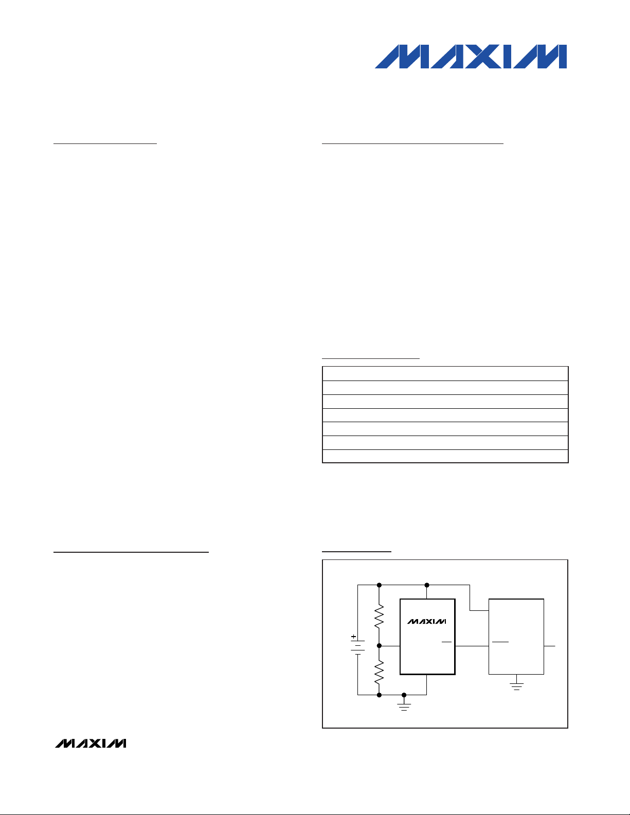
Ordering Information
LBI
3.6V
LBO
BATT
MAX6775
SHDN OUT
DC-DC
CONVERTER
IN
Typical Operating Circuit
19-3774; Rev 0; 8/05
For pricing, delivery, and ordering information, please contact Maxim/Dallas Direct! at
1-888-629-4642, or visit Maxim’s website at www.maxim-ic.com.
Ordering Information continued at end of data sheet.
+Denotes lead-free package.
*Future product—contact factory for availability.
MAX6775/MAX6776/MAX6779/MAX6780/MAX6781 are available
with factory-trimmed hysteresis. Specify trim by replacing “_”
with “A” for 0.5%, “B” for 5%, or “C” for 10% hysteresis.
Pin Configurations appear at end of data sheet.
PART TEMP RANGE PIN-PACKAGE
MAX6775XK_+T -40°C to +85°C 5 SC70-5
MAX6775LT_+T* -40°C to +85°C 6 µDFN-6
MAX6776XK_+T* -40°C to +85°C 5 SC70-5
MAX6776LT_+T* -40°C to +85°C 6 µDFN-6
MAX6777XK+T -40°C to +85°C 5 SC70-5
MAX6777LT+T* -40°C to +85°C 6 µDFN-6
Page 2
MAX6775–MAX6781
Low-Power, 1%-Accurate Battery
Monitor in µDFN and SC70 Packages
2 _______________________________________________________________________________________
ABSOLUTE MAXIMUM RATINGS
ELECTRICAL CHARACTERISTICS
(V
BATT
= 1.6V to 5.5V, TA= -40°C to +85°C, unless otherwise specified. Typical values are at TA= +25°C.) (Note 1)
Stresses beyond those listed under “Absolute Maximum Ratings” may cause permanent damage to the device. These are stress ratings only, and functional
operation of the device at these or any other conditions beyond those indicated in the operational sections of the specifications is not implied. Exposure to
absolute maximum rating conditions for extended periods may affect device reliability.
BATT to GND............................................................-0.3V to +6V
LBI, LBL, LBH, LBI1, LBI2 to GND ...............-0.3V to minimum of
((V
BATT
+ 0.3V) and +6V)
LBO, LBO1, LBO2 to GND (open-drain) .................-0.3V to +6V
LBO, LBO1, LBO2 to GND (push-pull).........-0.3V to minimum of
((V
BATT
+ 0.3V) and +6V)
Input Current (all pins) ........................................................20mA
Output Current (all pins) .....................................................20mA
Continuous Power Dissipation (T
A
= +70°C)
5-Pin SC70 (derate 3.1mW/°C above +70°C)..............247mW
6-Pin µDFN (derate 2.1mW°C above +70°C) ..............168mW
Junction Temperature......................................................+150°C
Storage Temperature Range .............................-65°C to +150°C
Lead Temperature (soldering, 10s) .................................+300°C
PARAMETER
CONDITIONS MIN TYP MAX
UNITS
TA = 0°C to +70°C 1.0 5.5
Operating Voltage Range
(Note 2)
TA = -40°C to +85°C 1.2 5.5
V
V
BATT
= 3.7V, no load 4 7
Supply Current I
Q
V
BATT
= 1.8V, no load 3.2 6
µA
FIXED HYSTERESIS (MAX6775/MAX6776/MAX6779/MAX6780/MAX6781)
0.5% hysteresis version
5% hysteresis version
LBI, LBI_ Falling Threshold
(Note 3)
V
LBIF
10% hysteresis version
V
LBI Rising Threshold V
LBIR
1.222
V
LBI Input Leakage Current 0.2V ≤ V
LBI
≤ V
BATT
- 0.2V -5 +5 nA
ADJUSTABLE HYSTERESIS (MAX6777/MAX6778)
LBL, LBH Threshold V
BATT
= 1.8V to 5.5V
1.222
V
LBL, LBH Input Leakage Current
V
BATT
- 0.2V ≥ V
LBL/LBH
≥ 0.2V -5 +5 nA
SYMBOL
V
BATT
1.2037 1.2159 1.2280
1.1493 1.1609 1.1725
1.0888 1.0998 1.1108
1.2098
1.2098
1.2342
1.2342
Page 3
MAX6775–MAX6781
Low-Power, 1%-Accurate Battery
Monitor in µDFN and SC70 Packages
_______________________________________________________________________________________ 3
ELECTRICAL CHARACTERISTICS (continued)
(V
BATT
= 1.6V to 5.5V, TA= -40°C to +85°C, unless otherwise specified. Typical values are at TA= +25°C.) (Note 1)
Note 1: Devices are tested at T
A
= +25°C and guaranteed by design for TA=T
MIN
to T
MAX
, as specified.
Note 2: Operating range ensures low-battery output is in the correct state. Minimum battery voltage for electrical specification is 1.6V.
Note 3: The rising threshold is guaranteed to be higher than the falling threshold.
PARAMETER
SYMBOL
CONDITIONS MIN TYP MAX
UNITS
LOW-BATTERY OUTPUTS (LBO, LBO1, LBO2)
Propagation Delay t
PD
V
LBI_
+ 100mV to V
LBI_
- 100mV 9 µs
Startup Time V
BATT
rising above 1.6V 3 ms
V
BATT
≥ 1.2V, I
SINK
= 100µA 0.3
V
BATT
≥ 2.7V, I
SINK
= 1.2mA 0.3
Output Low (Push-Pull or
Open-Drain)
V
OL
V
BATT
≥ 4.5V, I
SINK
= 3.2mA 0.3
V
V
BATT
≥ 1.6V, I
SOURCE
= 100µA
0.8 x
V
BATT
≥ 2.7V, I
SOURCE
= 500µA
0.8 x
Output High (Push-Pull ) V
OH
V
BATT
≥ 4.5V, I
SOURCE
= 800µA
0.8 x
V
Output Leakage Current
(Open-Drain)
Output not asserted, V
LBO_
= 5.5V -100 +100 nA
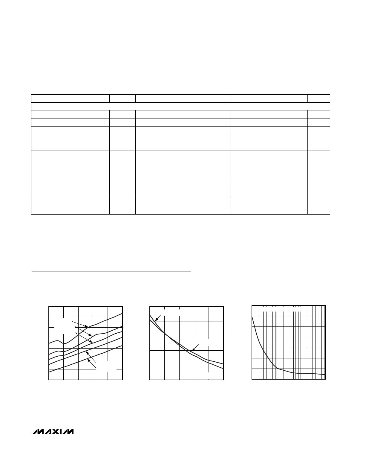
Typical Operating Characteristics
(TA = +25°C, unless otherwise noted.)
SUPPLY CURRENT
vs. TEMPERATURE
MAX6775 toc01
TEMPERATURE (°C)
SUPPLY CURRENT (µA)
603510-15
3.0
3.5
4.0
4.5
5.0
5.5
6.0
2.5
-40 85
V
BATT
= 5V
V
BATT
= 3.6V
V
BATT
= 3V
V
BATT
= 2.4V
V
BATT
= 1.6V
PROPAGATION DELAY
vs. TEMPERATURE
MAX6775 toc02
TEMPERATURE (°C)
PROPAGATION DELAY (µs)
603510-15
8
9
10
11
12
7
-40 85
V
BATT
= 5V
100mV OVERDRIVE
V
BATT
= 1.6V
MAXIMUM TRANSIENT DURATION
vs. THRESHOLD OVERDRIVE
MAX6775 toc03
THRESHOLD OVERDRIVE VTH - VCC (mV)
MAXIMUM TRANSIENT DURATION (µs)
10010
10
20
30
40
50
60
70
0
1 1000
OUTPUT ASSERTED ABOVE THIS LINE
V
BATT
V
BATT
V
BATT
Page 4
MAX6775–MAX6781
Low-Power, 1%-Accurate Battery
Monitor in µDFN and SC70 Packages
4 _______________________________________________________________________________________
Typical Operating Characteristics (continued)
(TA = +25°C, unless otherwise noted.)
NORMALIZED THRESHOLD VOLTAGES
vs. TEMPERATURE, MAX67__A
MAX6775 toc04
TEMPERATURE (°C)
THRESHOLD VOLTAGE (mV)
603510-15
-4
-3
-2
-1
0
1
-5
-40 85
NORMALIZED AT TA = +25°C
RISING
FALLING
NORMALIZED THRESHOLD VOLTAGES
vs. TEMPERATURE, MAX67__B
MAX6775 toc05
TEMPERATURE (°C)
THRESHOLD VOLTAGE (mV)
603510-15
-3
-2
-1
0
1
-4
-40 85
NORMALIZED AT TA = +25°C
RISING
FALLING
NORMALIZED THRESHOLD VOLTAGES
vs. TEMPERATURE, MAX67__C
MAX6775 toc06
TEMPERATURE (°C)
THRESHOLD VOLTAGE (mV)
603510-15
-2
-1
0
1
-3
-40 85
NORMALIZED AT TA = +25°C
RISING
FALLING
LBO OUTPUT VOLTAGE
vs. SINK CURRENT
MAX6775 toc07
SINK CURRENT (mA)
OUTPUT VOLTAGE (V)
12963
0.1
0.2
0.3
0.4
0.5
0
015
V
BATT
= 5.0V
V
BATT
= 1.8V
V
BATT
= 3.3V
LBO OUTPUT VOLTAGE
vs. SOURCE CURRENT
MAX6775 toc08
SOURCE CURRENT (mA)
OUTPUT VOLTAGE (V)
4321
1.5
2.0
2.5
3.0
3.5
4.0
4.5
5.0
5.5
1.0
05
V
BATT
= 5.0V
V
BATT
= 3.3V
V
BATT
= 1.8V
Page 5

MAX6775–MAX6781
Low-Power, 1%-Accurate Battery
Monitor in µDFN and SC70 Packages
_______________________________________________________________________________________ 5
Pin Description
MAX6775/
MAX6776
MAX6777/
MAX6778
MAX6779/
µDFN
µDFN
NAME FUNCTION
11—— — GND2
Reserved. Must be connected to GND. Do not use as the only
GND connection.
2222 2 GND Ground
33—— — LBI
Low-Battery Input. Connect to the resistive divider to set the
trip level.
4444 — LBO
Low-Battery Output, Active-Low. When V
LBI/VLBL
falls below
the falling threshold, LBO asserts. LBO deasserts when
V
LBI/VLBH
exceeds the rising threshold voltage.
5—5— — N.C. No Connection. Not internally connected.
6565 6 BATT Battery Input. Power supply to the device.
——1 1 — LBH
Rising-Trip-Level Input. Connect to a resistive divider to set the
rising trip level.
——3 3 — LBL
Falling-Trip-Level Input. Connect to a resistive divider to set the
falling trip level.
———— 1 LBI2
Low-Battery Input 2. Connect to a resistive divider to set the
trip level.
———— 3 LBI1
Low-Battery Input 1. Connect to a resistive divider to set the
trip level.
———— 4 LBO1
Low-Battery Output 1, Active-Low. When V
LBI1
falls below the
falling threshold voltage, LBO1 asserts. LBO1 deasserts when
V
LBI1
exceeds the rising threshold voltage. LBO1 is push-pull
on the MAX6781 and open-drain for the MAX6779/MAX6780.
———— 5 LBO2
Low-Battery Output 2, Active-Low. When V
LBI2
falls below the
falling threshold voltage, LBO2 asserts. LBO2 deasserts when
V
LBI2
exceeds the rising threshold voltage. LBO2 is open-drain.
SC70 µDFN SC70
MAX6780/
MAX6781
Page 6

MAX6775–MAX6781
Detailed Description
These battery monitors have an active-low output that
asserts when the input falls below a set voltage. They
also offer hysteresis for noise immunity, and to remove
the possibility of output chatter due to battery terminal
voltage recovery after load removal. They are available
with one or two monitors per package, with push-pull or
open-drain outputs, and with internally set or externally
adjustable hysteresis (dual-channel devices offer only
internally fixed hysteresis). Figures 1, 2, and 3 show
block diagrams and typical connections. See the
Selector Guide for details.
Low-Battery Output
All devices are offered with either push-pull or opendrain outputs (see the Selector Guide). The MAX6781
has one push-pull output and one open-drain output,
configured as in Table 1.
On all devices with open-drain outputs an external
pullup resistor is required. The open-drain pullup resistor can connect to an external voltage up to +6V,
regardless of the voltage at BATT.
Low-Power, 1%-Accurate Battery
Monitor in µDFN and SC70 Packages
6 _______________________________________________________________________________________
Table 1. MAX6781 Outputs
DEVICE LBO1 LBO2
MAX6781 Push-Pull Open-Drain
Figure 2. Dual-Channel Fixed-Hysteresis Block Diagram
LBI
LBO
0
1
BATT
GND
R
L
V
REF
V
BATT
R
H
MAX6775
MAX6776
HYSTERESIS
CONTROL
Figure 1. Single-Channel Fixed-Hysteresis Block Diagram
LBL
LBO
0
1
LBH
BATT
GND
R
HYST
V
REF
V
BATT
R
H
R
L
MAX6777
MAX6778
Figure 3. Single-Channel Adjustable-Hysteresis Block Diagram
V
BATT
LBI1
HYSTERESIS
CONTROL
LBI2
GND
BATT
MAX6779
MAX6780
MAX6781
1
0
V
REF
0
1
LBO1
LBO2
Page 7

MAX6775–MAX6781
Low-Power, 1%-Accurate Battery
Monitor in µDFN and SC70 Packages
_______________________________________________________________________________________ 7
The MAX6779, MAX6780, and MAX6781 monitor two
battery levels or two independent voltages. A common
application for this type of dual-battery monitor is to use
one output as an early warning signal and the other as
a dead-battery indicator.
Hysteresis
Input hysteresis defines two thresholds, separated by a
small voltage (the hysteresis voltage), configured so
the output asserts when the input falls below the falling
threshold, and deasserts only when the input rises above
the rising threshold. Figure 4 shows this graphically.
Hysteresis removes, or greatly reduces, the possibility of
the output changing state in response to noise or battery
terminal voltage recovery after load removal.
Fixed Hysteresis
The MAX6775/MAX6776/MAX6779/MAX6780/MAX6781
have factory-set hysteresis for ease of use, and reduce
component count. For these devices, the absolute hysteresis voltage is a percentage of the internally generated reference. The amount depends on the device
option. “A” devices have 0.5% hysteresis, “B” devices
have 5% hysteresis, and “C” devices have 10% hysteresis. Table 2 presents the threshold voltages for devices
with internally fixed hysteresis.
Adjustable Hysteresis
The MAX6777/MAX6778 offer external hysteresis control through the resistive divider that monitors battery
voltage. Figure 3 shows the connections for external
hysteresis. See the Calculating an External Hysteresis
Resistive Divider section for more information.
Applications Information
Resistor-Value Selection
Choosing the proper external resistors is a balance
between accuracy and power use. The input to the voltage monitor, while high impedance, draws a small current, and that current travels through the resistive
divider, introducing error. If extremely high resistor values are used, this current introduces significant error.
With extremely low resistor values, the error becomes
negligible, but the resistive divider draws more power
from the battery than necessary and shortens battery
life. Figure 1 calculates the optimum value for RHusing:
where eAis the maximum acceptable absolute resistive
divider error (use 0.01 for 1%), V
BATT
is the battery volt-
age at which LBO should activate, and ILis the worstcase LBI leakage current. For example, with 0.5%
accuracy, a 2.8V battery minimum, and 5nA leakage,
RH= 2.80MΩ.
Calculate RLusing:
where V
LBIF
is the falling threshold voltage from Table 2.
Continuing the above example, select V
LBIF
= 1.0998V
(10% hysteresis device) and RL= 1.81MΩ.
R
VxR
VV
L
LBIF H
LBIF BATT
= −
−
R
exV
I
H
A BATT
L
=
V
BATT
LBO
V
LBIR
V
LBIF
V
HYST
t
PD
t
PD
MAX6775
MAX6776
Figure 4. Hysteresis
Table 2. Typical Falling and Rising Thresholds for
MAX6775/MAX6776/MAX6779/MAX6780/MAX6781
DEVICE OPTION
PERCENT
FALLING THRESHOLD
(V
LBIF
) (V)
RISING THRESHOLD
(V
LBIR
) (V)
HYSTERESIS VOLTAGE
(V
HYST
) (mV)
A 0.5 1.2159 1.222 6.11
B5 1.1609 1.222 61.1
C10 1.0998 1.222 122
HYSTERESIS (%)
Page 8

MAX6775–MAX6781
Low-Power, 1%-Accurate Battery
Monitor in µDFN and SC70 Packages
8 _______________________________________________________________________________________
Selector Guide
PART LBO OUTPUT OUTPUT TYPE HYSTERESIS PIN-PACKAGE
MAX6775XK_+T Single Push-Pull Fixed 5 SC70-5
MAX6775LT_+T Single Push-Pull Fixed 6 µDFN-6
MAX6776XK_+T Single Open-Drain Fixed 5 SC70-5
MAX6776LT_+T Single Open-Drain Fixed 6 µDFN-6
MAX6777XK+T Single Push-Pull Adjustable 5 SC70-5
MAX6777LT+T Single Push-Pull Adjustable 6 µDFN-6
MAX6778XK+T Single Open-Drain Adjustable 5 SC70-5
MAX6778LT+T Single Open-Drain Adjustable 6 µDFN-6
MAX6779LT_+T Dual Push-Pull Fixed 6 µDFN-6
MAX6780LT_+T Dual Open-Drain Fixed 6 µDFN-6
MAX6781LT_+T Dual Mixed Fixed 6 µDFN-6
Calculating an External
Hysteresis Resistive Divider
Setting the hysteresis externally requires calculating
three resistor values, as indicated in Figure 3. First calculate RHusing:
and RL0using:
(as in the above example). Where RL0equals RL+
R
HYST
, determine the total resistor-divider current,
I
TOTAL
, at the trip voltage using:
Then, determine R
HYST
using:
where V
HYST
is the required hysteresis voltage.
Finally, determine RLusing:
RL= RL0- R
HYST
Monitoring a Battery Voltage Higher
Than the Allowable V
BATT
For monitoring higher voltages, supply power to BATT
that is within the specified supply range, and power the
input resistive divider from the high voltage to be monitored. Do not exceed the Absolute Maximum Ratings.
Adding External Capacitance to
Reduce Noise and Transients
If monitoring voltages in a noisy environment, add a
bypass capacitor of 0.1µF from BATT to GND as close
as possible to the device. For systems with large transients, additional capacitance may be required. A small
capacitor (<1nF) from LBI_ to GND may provide additional noise immunity.
R
V
I
HYST
HYST
TOTAL
=
I
V
RR
TOTAL
BATT
HL
=+
0
R
VxR
VV
L
LBIR H
LBIR BATT
0
=
−
−
R
exV
I
H
A BATT
L
=
Page 9

MAX6775–MAX6781
Low-Power, 1%-Accurate Battery
Monitor in µDFN and SC70 Packages
_______________________________________________________________________________________ 9
Top Marks
PART TOP MARK
MAX6775XKA+T ASA
MAX6775XKB+T ASB
MAX6775XKC+T ASC
MAX6775LTA+T BU
MAX6775LTB+T BW
MAX6775LTC+T BX
MAX6776XKA+T ASJ
MAX6776XKB+T ASK
MAX6776XKC+T ASL
MAX6776LTA+T BY
MAX6776LTB+T BZ
MAX6776LTC+T CA
Ordering Information (continued)
PART TEMP RANGE PIN-PACKAGE
MAX6778XK+T* -40°C to +85°C 5 SC70-5
MAX6778LT+T* -40°C to +85°C 6 µDFN-6
MAX6779LT_+T* -40°C to +85°C 6 µDFN-6
MAX6780LT_+T* -40°C to +85°C 6 µDFN-6
MAX6781LT_+T* -40°C to +85°C 6 µDFN-6
+Denotes lead-free package.
*Future product—contact factory for availability.
MAX6775/MAX6776/MAX6779/MAX6780/MAX6781 are available
with factory-trimmed hysteresis. Specify trim by replacing “_”
with “A” for 0.5%, “B” for 5%, or “C” for 10% hysteresis.
Chip Information
PROCESS: BICMOS
TRANSISTOR COUNT: 496
PART TOP MARK
MAX6777XK+T ASD
MAX6777LT+T CB
MAX6778XK+T ASI
MAX6778LT+T CC
MAX6779LTA+T BL
MAX6779LTB+T BM
MAX6779LTC+T BN
MAX6780LTA+T BO
MAX6780LTB+T BP
MAX6780LTC+T BQ
MAX6781LTA+T BR
MAX6781LTB+T BS
MAX6781LTC+T BT
Page 10

MAX6775–MAX6781
Low-Power, 1%-Accurate Battery
Monitor in µDFN and SC70 Packages
10 ______________________________________________________________________________________
GND
LBOLBI
15BATTGND2
MAX6775
MAX6776
SC70-5
+
+
TOP VIEW
2
34
123
456
BATT LBON.C.
GND2 LBIGND
MAX6775
MAX6776
µDFN-6
123
456
BATT LBON.C.
LBH LBLGND
MAX6777
MAX6778
µDFN-6
123
456
BATT LBO1LBO2
LBI2 LBI1GND
MAX6779
MAX6780
MAX6781
µDFN-6
GND
LBOLBL
15BATTLBH
MAX6777
MAX6778
SC70-5
2
34
Pin Configurations
Page 11

MAX6775–MAX6781
Low-Power, 1%-Accurate Battery
Monitor in µDFN and SC70 Packages
______________________________________________________________________________________ 11
Package Information
(The package drawing(s) in this data sheet may not reflect the most current specifications. For the latest package outline information,
go to www.maxim-ic.com/packages
.)
6L UDFN.EPS
L
TOP VIEW
D
E
SIDE VIEW
A1
PIN 1
INDEX AREA
A
A 0.64
COMMON DIMENSIONS
PIN 1
0.075x45°
BOTTOM VIEW
L1
32
MIN.
1
e
6
5
b
4
SECTION A-A
b
L2
A A
NOM.
0.72 0.80
MAX.
0.20--A1 --
1.501.45D 1.55
1.000.95E 1.05
0.350.30L 0.40
----L1 0.08
----L2 0.05
0.200.17b 0.23
0.50 BSC.e
AAA
TOPMARK
2
1
-DRAWING NOT TO SCALE-
DOCUMENT CONTROL NO.APPROVAL
TITLE:
REV.
PACKAGE OUTLINE, 6L uDFN, 1.5x1.0x0.8mm
21-0147
1
1
C
3
Page 12

MAX6775–MAX6781
Low-Power, 1%-Accurate Battery
Monitor in µDFN and SC70 Packages
Maxim cannot assume responsibility for use of any circuitry other than circuitry entirely embodied in a Maxim product. No circuit patent licenses are
implied. Maxim reserves the right to change the circuitry and specifications without notice at any time.
12 ____________________Maxim Integrated Products, 120 San Gabriel Drive, Sunnyvale, CA 94086 408-737-7600
© 2005 Maxim Integrated Products Printed USA is a registered trademark of Maxim Integrated Products, Inc.
Heaney
Package Information (continued)
(The package drawing(s) in this data sheet may not reflect the most current specifications. For the latest package outline information,
go to www.maxim-ic.com/packages
.)
SC70, 5L.EPS
PACKAGE OUTLINE, 5L SC70
21-0076
1
1
C
 Loading...