

Page 1
General Description
The MAX6754–MAX6764 low-power window detectors
monitor undervoltage/overvoltage conditions on system
power supplies. These devices assert when the monitored voltage is under the undervoltage and/or over the
overvoltage thresholds.
The MAX6754–MAX6759/MAX6763/MAX6764 monitor a
single voltage. The MAX6760/MAX6761/MAX6762
monitor dual-voltage systems. The MAX6754/MAX6755/
MAX6756 provide a single undervoltage/overvoltage
output and the MAX6757–MAX6764 provide independent undervoltage and overvoltage outputs. The outputs are available in push-pull or open-drain
configurations.
The MAX6754–MAX6762 offer factory-fixed voltage
thresholds for monitoring system voltages from 0.9V to
5V with a selectable ±5%, ±10%, or ±15% window voltage. The MAX6763/MAX6764 allow for externally
adjustable thresholds. The MAX6754–MAX6762 are
available in two delay timing options (20µs, typ or
100ms, min). The MAX6760/MAX6761/MAX6762 also
include a latched overvoltage output function and the
MAX6754–MAX6762 include a manual reset input.
The family of products is available in small SOT23 and
TDFN packages and is specified over the extended
temperature range of -40°C to +125°C.
Applications
Features
♦ Single- or Dual-Supply Voltage Monitors
♦ Factory-Trimmed Window Threshold Options for
5V, 3.3V, 3V, 2.5V, 1.8V, 1.5V, 1.2V, and 0.9V
Supplies
♦ Externally Adjustable Window Monitoring Options
for Supplies Down to 0.5V
♦ Selectable Window Threshold Options (±5%,
±10%, ±15%)
♦ Single (Combined UV/OV) or Dual (Separate UV
and OV) Outputs
♦ 20µs (typ) or 100ms (min) Timeout Period Options
(MAX6754–MAX6762)
♦ Manual Reset Input (MAX6754–MAX6762)
♦ Latched Overvoltage Output Function
(MAX6760/MAX6761/MAX6762)
♦ Immune to Short Voltage Transients
♦ Low 10µA Supply Current
♦ Low-Voltage Operation (Outputs Valid for V
CC
Down to 1V)
♦ -40°C to +125°C Operating Temperature Range
♦ Small SOT23 and TDFN Packages
MAX6754–MAX6764
Low-Power, Single/Dual-Voltage Window
Detectors
________________________________________________________________ Maxim Integrated Products 1
Ordering Information
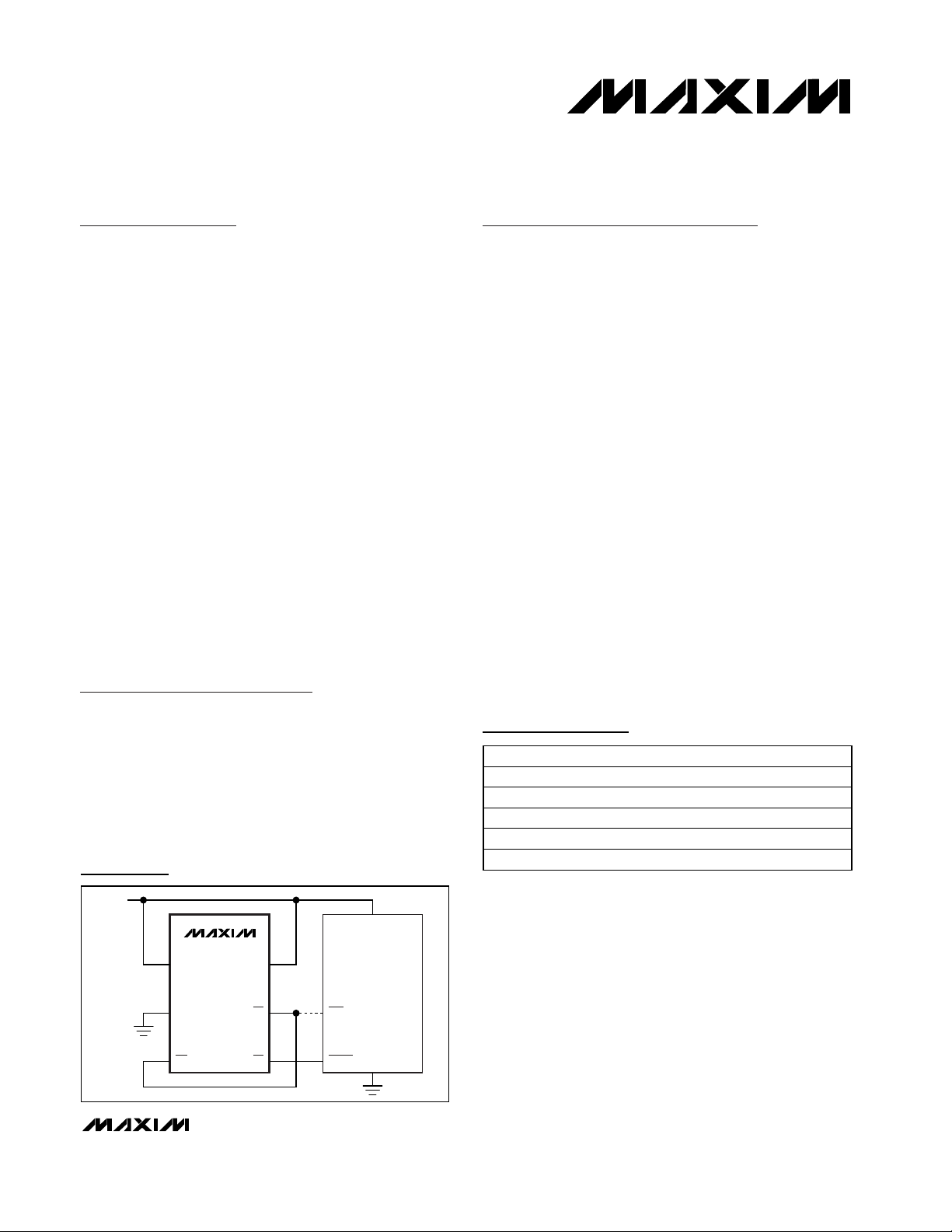
MAX6757
NMI
RESETMR
GND
V
CC
UV
OV
SET
V
CC
µP
Typical Application Circuit
19-3031; Rev 0; 10/03
For pricing, delivery, and ordering information, please contact Maxim/Dallas Direct! at
1-888-629-4642, or visit Maxim’s website at www.maxim-ic.com.
*Note: Insert the threshold level suffixes for VCCand V
CC2
(Tables 1 and 2) after UK, UT, or TA. For the
MAX6754–MAX6759, insert only the VCCthreshold suffix after
the UK or UT. Insert the reset timeout delay (Table 3) after D to
complete the part number. For example, the MAX6760TALTD3-T
provides a V
CC
threshold of 5V, a V
CC2
threshold of 3.3V, and a
100ms minimum reset timeout period. Sample stock is generally
held on standard versions only (see the Standard Versions
table). Standard versions have an order increment requirement
of 2500 pieces. Nonstandard versions have an order increment
requirement of 10,000 pieces. Contact factory for availability.
Ordering Information continued at end of data sheet.
Pin Configurations appear at end of data sheet.
Telecommunications
Networking
Computers/Servers
Data Storage
Power Metering
DC-DC Converter
Modules
Automotive
PART* TEMP RANGE PIN-PACKAGE
MAX6754UK_D_-T -40°C to +125°C 5 SOT23-5
MAX6755UK_D_-T -40°C to +125°C 5 SOT23-5
MAX6756UK_D_-T -40°C to +125°C 5 SOT23-5
MAX6757UT_D_-T -40°C to +125°C 6 SOT23-6
MAX6758UT_D_-T -40°C to +125°C 6 SOT23-6
Page 2
MAX6754–MAX6764
Low-Power, Single/Dual-Voltage Window
Detectors
2 _______________________________________________________________________________________
ABSOLUTE MAXIMUM RATINGS
ELECTRICAL CHARACTERISTICS
(V
CC
= 1.0V to 6.0V, V
CC2
= 0 to 6.0V (MAX6760–MAX6762), TA= -40°C to +125°C, unless otherwise noted. Typical values are at TA=
+25°C.) (Note 1)
Stresses beyond those listed under “Absolute Maximum Ratings” may cause permanent damage to the device. These are stress ratings only, and functional
operation of the device at these or any other conditions beyond those indicated in the operational sections of the specifications is not implied. Exposure to
absolute maximum rating conditions for extended periods may affect device reliability.
(Voltages with respect to GND)
V
CC
, V
CC2
, ............................................................-0.3V to +6.5V
SET, OVLATCH, MR, UVIN, OVIN ..............-0.3V to (V
CC
+ 0.3V)
UV, RESET, OV (open drain) .................................-0.3V to +6.5V
RESET, OV, UV, UV, RESET (push-pull).....-0.3V to (V
CC
+ 0.3V)
Input/Output Current (all pins) ............................................20mA
Continuous Power Dissipation (T
A
= +70°C)
5-Pin SOT23-5 (derate 7.1mW/°C above T
A
= +70°C)....571mW
6-Pin SOT23-6 (derate 8.7mW/°C above T
A
= +70°C)....696mW
8-Pin TDFN (derate 24.4mW/°C above T
A
= +70°C).....1951mW
Operating Temperature Range .........................-40°C to +125°C
Junction Temperature......................................................+150°C
Storage Temperature Range .............................-65°C to +150°C
Lead Temperature (soldering, 10s) .................................+300°C
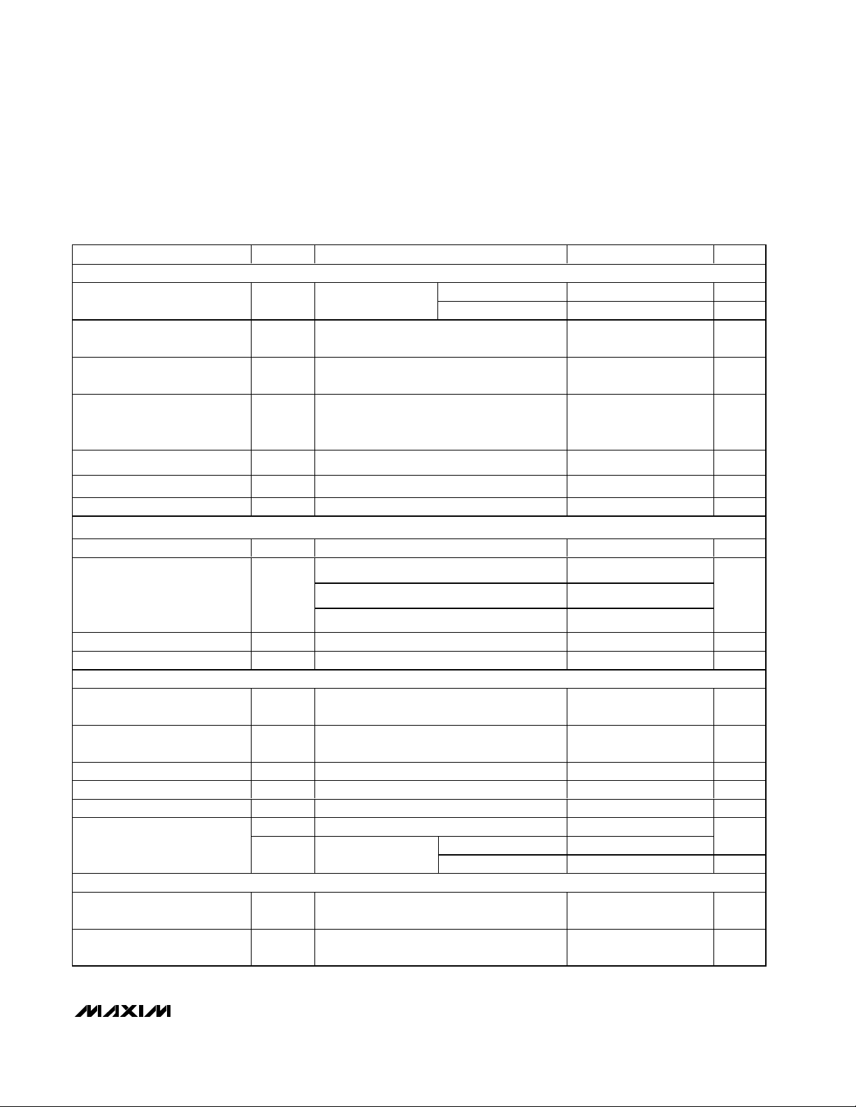
PARAMETER SYMBOL CONDITIONS MIN TYP MAX UNITS
POWER REQUIREMENTS
Operating Voltage Range V
VCC Supply Current I
V
Supply Current
CC2
Adjustable Bias Current
V
THRESHOLD
CC
VCC Overvoltage Threshold OV
(Note 2) 1.0 6.0
CC
MAX6760TAAA/MAX6761TAAA/
MAX6762TAAA/MAX6763/MAX6764UT-T
VCC = 3.6V, MAX6754–MAX6759, no load 13 30
VCC = 3.6V, MAX6763/MAX6764, no load 10 23
CC
VCC = 3.6V, VCC ≥ V
CC2
,
MAX6760/MAX6761/MAX6762, no load
V
I
CC2
= 1.8V, VCC ≥ V
CC2
MAX6760/MAX6761/MAX6762
V
(MAX6760–MAX6762TA_AD_)
CC2
CC2
,
(Note 3)
V
= V
SET
SB
L, 5V
SET = V
CC
SET = GND 5.250 5.375 5.500
V
= V
SET
SB
SET = V
CC
SET = GND 3.465 3.548 3.630
V
= V
SET
SET
= V
SB
CC
SB
CC
TH
TA = -40°C to
+125°C,
rising V
CC
R, 3.0V
Z, 2.5V
SET = V
SET = GND 3.150 3.225 3.300
V
SET = V
SET = GND 2.625 2.688 2.750
V
= V
SET
SB
W, 1.8V
SET = V
CC
SET = GND 1.890 1.935 1.980
1.4 6.0
13 30
1 1.5 µA
-20 +20 nA
5.750 5.875 6.000
5.500 5.625 5.750
3.795 3.878 3.960
3.630 3.713 3.795T, 3.3V
3.450 3.525 3.600
3.300 3.375 3.450
2.875 2.938 3.000
2.750 2.813 2.875
2.070 2.115 2.160
1.980 2.025 2.070
V
µA
V
Page 3
MAX6754–MAX6764
Low-Power, Single/Dual-Voltage Window
Detectors
_______________________________________________________________________________________ 3
ELECTRICAL CHARACTERISTICS (continued)
(V
CC
= 1.0V to 6.0V, V
CC2
= 0 to 6.0V (MAX6760–MAX6762), TA= -40°C to +125°C, unless otherwise noted. Typical values are at TA=
+25°C.) (Note 1)
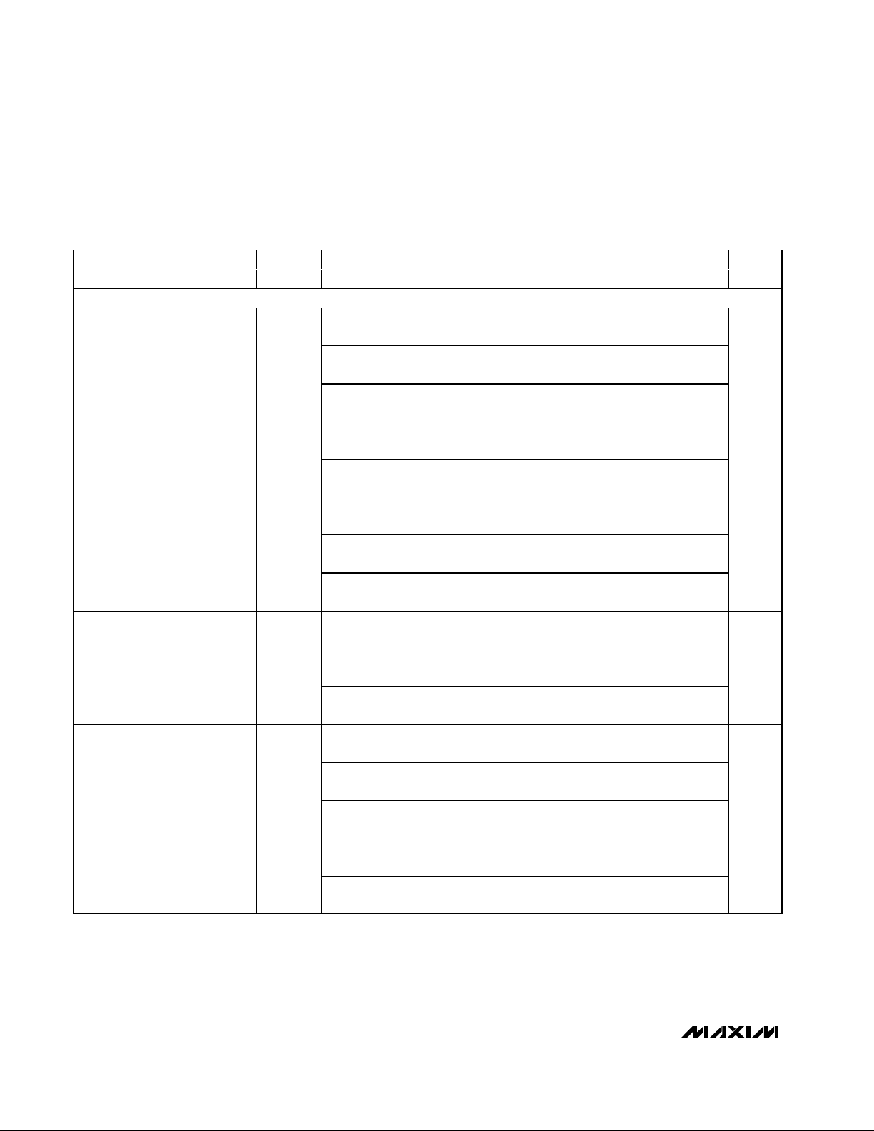
PARAMETER SYMBOL CONDITIONS MIN TYP MAX UNITS
VCC Undervoltage Threshold UV
V
Overvoltage Threshold OV
CC2
L, 5V
TA = -40°C
TH
to +125°C,
falling V
R, 3.0V
CC
W, 1.8V
T, 3.3V
W, 1.8V
TA = -40°C
to +125°C,
TH2
rising V
CC2
G, 1.2V
ADJ
V
= V
SET
SET = V
SB
CC
4.000 4.125 4.250
4.250 4.375 4.500
SET = GND 4.500 4.625 4.750
V
= V
SET
SET = V
SB
CC
2.640 2.723 2.805
2.805 2.888 2.970T, 3.3V
SET = GND 2.970 3.053 3.135
V
= V
SET
SET = V
SB
CC
2.400 2.475 2.550
2.550 2.625 2.700
SET = GND 2.700 2.775 2.850
V
= V
SET
SET = V
SB
CC
2.000 2.063 2.125
2.125 2.188 2.250Z, 2.5V
SET = GND 2.250 2.313 2.375
V
= V
SET
SET = V
SB
CC
1.440 1.485 1.530
1.530 1.575 1.620
SET = GND 1.620 1.665 1.710
V
= V
SET
SET = V
SB
CC
3.795 3.878 3.960
3.630 3.713 3.795
SET = GND 3.465 3.548 3.630
V
= V
SET
SET = V
SB
CC
3.450 3.525 3.600
3.300 3.375 3.450R, 3.0V
SET = GND 3.150 3.225 3.300
V
= V
SET
SET = V
SB
CC
2.875 2.938 3.000
2.750 2.813 2.875Z, 2.5V
SET = GND 2.625 2.688 2.750
V
= V
SET
SET = V
SB
CC
2.070 2.115 2.160
1.980 2.025 2.070
SET = GND 1.890 1.935 1.980
V
= VSB (Note 2) 1.725 1.763 1.800
SET
SET = VCC (Note 2) 1.650 1.688 1.725I, 1.5V
SET = GND (Note 2) 1.575 1.613 1.650
V
= VSB (Note 2) 1.380 1.410 1.440
SET
SET = VCC (Note 2) 1.320 1.350 1.380
SET = GND (Note 2) 1.260 1.290 1.320
V
= VSB (Note 2) 1.035 1.058 1.080
SET
SET = VCC (Note 2) 0.990 1.013 1.035E, 0.9V
SET = GND (Note 2) 0.945 0.968 0.990
V
= V
SET
SET = V
SB
CC
0.489 0.500 0.511
0.468 0.479 0.489
SET = GND 0.447 0.457 0.468
V
V
Page 4
MAX6754–MAX6764
Low-Power, Single/Dual-Voltage Window
Detectors
4 _______________________________________________________________________________________
ELECTRICAL CHARACTERISTICS (continued)
(V
CC
= 1.0V to 6.0V, V
CC2
= 0 to 6.0V (MAX6760–MAX6762), TA= -40°C to +125°C, unless otherwise noted. Typical values are at TA=
+25°C.) (Note 1)
V
Threshold Hysteresis V
UNDERVOLTAGE/OVERVOLTAGE INPUTS (UVIN, OVIN) (MAX6763/MAX6764)
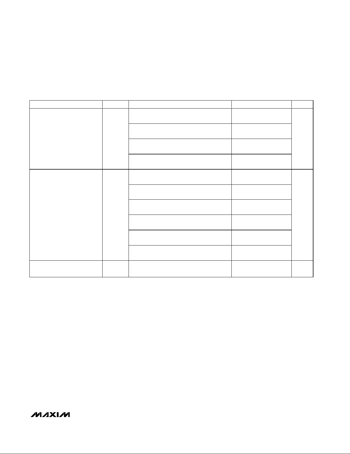
PARAMETER SYMBOL CONDITIONS MIN TYP MAX UNITS
Undervoltage Threshold UV
CC2
V
TA = -40°C
to +125°C,
TH2
falling V
HYSTVCC
, V
CC2
CC2
T, 3.3V
Z, 2.5V
G, 1.2V
ADJ
= V
SET
SB
SET = V
CC
SET = GND 2.970 3.053 3.135
V
= V
SET
SB
SET = V
CC
SET = GND 2.700 2.775 2.850
V
= V
SET
SB
SET = V
CC
SET = GND 2.250 2.313 2.375
V
= V
SET
SB
SET = V
CC
SET = GND 1.620 1.665 1.710
V
= VSB (Note 2) 1.200 1.238 1.275
SET
SET = VCC (Note 2) 1.275 1.313 1.350I, 1.5V
SET = GND (Note 2) 1.350 1.388 1.425
V
= VSB (Note 2) 0.960 0.990 1.020
SET
SET = VCC (Note 2) 1.020 1.050 1.080
SET = GND (Note 2) 1.080 1.110 1.140
V
= VSB (Note 2) 0.720 0.743 0.765
SET
SET = VCC (Note 2) 0.765 0.788 0.810E, 0.9V
SET = GND (Note 2) 0.810 0.833 0.855
V
= V
SET
SB
SET = V
CC
SET = GND 0.383 0.394 0.404
2.640 2.723 2.805
2.805 2.888 2.970
2.400 2.475 2.550
2.550 2.625 2.700R, 3.0V
2.000 2.063 2.125
2.125 2.188 2.250
1.440 1.485 1.530
1.530 1.575 1.620W, 1.8V
0.340 0.351 0.362
0.362 0.372 0.383
V
0.7 %
UVIN, OVIN Threshold Voltage V
UVIN, OVIN Input Bias Current I
UVIN, OVIN Threshold
Hysteresis
V
TH-IN
IN
HYST
0.4875 0.5 0.5125 V
-10 +10 nA
0.7 %
Page 5
MAX6754–MAX6764
Low-Power, Single/Dual-Voltage Window
Detectors
_______________________________________________________________________________________ 5
ELECTRICAL CHARACTERISTICS (continued)
(V
CC
= 1.0V to 6.0V, V
CC2
= 0 to 6.0V (MAX6760–MAX6762), TA= -40°C to +125°C, unless otherwise noted. Typical values are at TA=
+25°C.) (Note 1)
TIMING CHARACTERISTICS
Reset and UV Timeout Period t
VCC to Reset Delay t
VCC to UV Delay t
VCC to OV Delay t
UVIN to UV Delay (MAX6763/MAX6764) 20 µs
OVIN to OV Delay (MAX6763/MAX6764) 20 µs
Startup Delay Time t
THRESHOLD WINDOW SELECT INPUT (SET)
Input Voltage Low 0 0.1 V
Input Bias Voltage
(Note 5)
Input Voltage High VCC - 0.1 V
Input Current I
MANUAL RESET (MR)
Input Voltage Low
Input Voltage High
Pullup Resistance to V
Minimum Pulse Width 4µs
Transient Immunity 300 ns
Propagation Delay
OVERVOLTAGE OUTPUT LATCH CONTROL INPUT (OVLATCH)
Input Voltage Low
Input Voltage High
PARAMETER SYMBOL CONDITIONS MIN TYP MAX UNITS
D0 20 µs
D3 100 185 320 ms
20 µs
20 µs
20 µs
CC
-1 +1 µA
0.23 x
V
CC
0.6 x
V
CC
26 kΩ
D0 40
D3 100 185 320 ms
0.3 x
V
CC
0.7 x
V
CC
CC
RP
D-RESET
D-UV
D-OV
START
V
SB
SET
t
D-MR
t
MR_P
Figure 7
VCC/V
UV
VCC/V
OV
VCC/V
OV
(MAX6757–MAX6762 only)
D0 options only, OV output (Note 4) 2 ms
VCC = 1.4V 0.65 0.75
VCC = 3.0V 0.81 2.19
VCC = 6.0V 1.10 4.90
MR falling, Figure 7 300
MR rising, Figure 7
falling at 10mV/µs from
CC2
+ 100mV to UVTH - 100mV
TH
rising at 10mV/µs from
CC2
- 100mV to OVTH + 100mV
TH
rising at 10mV/µs from
CC2
- 100mV to OVTH + 100mV
TH
V
V
V
V
ns
V
V
Page 6
MAX6754–MAX6764
Low-Power, Single/Dual-Voltage Window
Detectors
6 _______________________________________________________________________________________
ELECTRICAL CHARACTERISTICS (continued)
(V
CC
= 1.0V to 6.0V, V
CC2
= 0 to 6.0V (MAX6760–MAX6762), TA= -40°C to +125°C, unless otherwise noted. Typical values are at TA=
+25°C.) (Note 1)
Input Bias Current I
RESET, RESET, UV, UV, OV
RESET, UV Output Low (Open
Drain or Push-Pull)
PARAMETER SYMBOL CONDITIONS MIN TYP MAX UNITS
RESET, UV Output High
(Push-Pull)
RESET, UV Output Low
(Push-Pull)
RESET, UV Output High
(Push-Pull)
OVLATCH
V
OL
V
OH
V
OL
V
OH
Any VCC ≥ 1.0V, I
output asserted
Any VCC ≥ 1.2V, I
output asserted
Any VCC ≥ 1.71V, I
output asserted
Any VCC ≥ 2.85V, I
output asserted
Any VCC ≥ 4.75V, I
output asserted
Any VCC ≥ 1.71V, I
output deasserted
Any VCC ≥ 2.85V, I
output deasserted
Any VCC ≥ 4.75V, I
output deasserted
Any VCC ≥ 1.71V, I
output deasserted
Any VCC ≥ 2.85V, I
output deasserted
Any VCC ≥ 4.75V, I
output deasserted
Any VCC ≥ 1.0V, I
output asserted
Any VCC ≥ 1.2V, I
output asserted
Any VCC ≥ 1.71V, I
output asserted
Any VCC ≥ 2.85V, I
output asserted
Any VCC ≥ 4.75V, I
output asserted
= 100µA,
SINK
= 200µA,
SINK
= 1.0mA,
SINK
= 2.0mA,
SINK
= 4.0mA,
SINK
SOURCE
SOURCE
SOURCE
= 1.0mA,
SINK
= 2.0mA,
SINK
= 4.0mA,
SINK
SOURCE
SOURCE
SOURCE
SOURCE
SOURCE
= 0.8mA,
= 2.0mA,
= 4.0mA,
= 50µA,
= 100µA,
= 0.8mA,
= 2.0mA,
= 4.0mA,
-1 +1 µA
0.8 x
V
CC
0.8 x
V
CC
0.8 x
V
CC
0.8 x
V
CC
0.8 x
V
CC
0.8 x
V
CC
0.8 x
V
CC
0.8 x
V
CC
0.3
0.3
0.3
0.3
0.3
0.3
0.3
0.3
V
V
V
V
Page 7
MAX6754–MAX6764
Low-Power, Single/Dual-Voltage Window
Detectors
_______________________________________________________________________________________ 7
ELECTRICAL CHARACTERISTICS (continued)
(V
CC
= 1.0V to 6.0V, V
CC2
= 0 to 6.0V (MAX6760–MAX6762), TA= -40°C to +125°C, unless otherwise noted. Typical values are at TA=
+25°C.) (Note 1)
Note 1: Devices are production tested at +25°C. Overtemperature limits are guaranteed by design.
Note 2: Voltage monitoring requires that V
CC
must be greater than or equal to 1.4V, but outputs remain asserted in the correct
state for V
CC
down to 1.0V.
Note 3: Guaranteed by design.
Note 4: For D0 window detector options and OV outputs, startup delay time is the time required for the internal reference/circuitry
to reach specified accuracy after the monitor is powered up from GND.
Note 5: The input bias voltage is based off of V
CC
. The minimum value is given by the equation (0.1 x V
CC
+ 0.51)V and the maxi-
mum value is given by (0.9 x V
CC
- 0.51)V.
OV Output Low
(Open-Drain or
Push-Pull)
OV Output High
(Push-Pull)
PARAMETER SYMBOL CONDITIONS MIN TYP MAX UNITS
Any VCC ≥ 1.98V, I
output asserted
Any VCC ≥ 2.75V, I
V
V
output asserted
OL
Any VCC ≥ 3.63V, I
output asserted
Any VCC ≥ 5.5V, I
output asserted
Any VCC ≥ 1.0V, I
output deasserted
Any VCC ≥ 1.2V, I
output deasserted
Any VCC ≥ 1.98V, I
output deasserted
OH
Any VCC ≥ 2.75V, I
output deasserted
Any VCC ≥ 3.63V, I
output deasserted
Any VCC ≥ 5.5V, I
output deasserted
SINK
SINK
SINK
SINK
SOURCE
SOURCE
SOURCE
SOURCE
SOURCE
SOURCE
= 1.4mA,
= 2.0mA,
= 3.0mA,
= 4.0mA,
= 50µA,
= 100µA,
= 1.4mA,
= 2.0mA,
= 3.0mA,
= 4.5mA,
0.8 x
V
CC
0.8 x
V
CC
0.8 x
V
CC
0.8 x
V
CC
0.8 x
V
CC
0.8 x
V
CC
0.3
0.3
V
0.3
0.3
V
RESET, UV, OV Output OpenDrain Leakage Current
I
LKG
Output not asserted 1 µA
Page 8

MAX6754–MAX6764
Low-Power, Single/Dual-Voltage Window
Detectors
8 _______________________________________________________________________________________
Typical Operating Characteristics
(VCC= 5V, V
CC2
= 3.3V, TA= +25°C, unless otherwise noted.)
OVERVOLTAGE THRESHOLD
vs. TEMPERATURE
MAX6754 toc01
TEMPERATURE (°C)
NORMALIZED OVERVOLTAGE THRESHOLD (V)
1109580655035205-10-25
0.98
0.99
1.00
1.01
1.02
1.03
0.97
-40 125
OVERVOLTAGE THRESHOLD RISING
OVERVOLTAGE THRESHOLD FALLING
NORMALIZED TO RISING
THRESHOLD AT T
A
= +25°C
UNDERVOLTAGE THRESHOLD
vs. TEMPERATURE
MAX6754 toc02
TEMPERATURE (°C)
NORMALIZED UNDERVOLTAGE THRESHOLD (V)
1109580655035205-10-25
0.98
0.99
1.00
1.01
1.02
1.03
0.97
-40 125
UNDERVOLTAGE THRESHOLD RISING
UNDERVOLTAGE THRESHOLD FALLING
NORMALIZED TO FALLING
THRESHOLD AT T
A
= +25°C
TRANSIENT IMMUNITY
vs. THRESHOLD OVERDRIVE
MAX6754 toc03
OVERDRIVE (mV)
TRANSIENT IMMUNITY (µs)
10010
100
10001
1000
10
OUTPUT ASSERTS
ABOVE THIS LINE
D3 TIMEOUT PERIOD
vs. TEMPERATURE
MAX6754 toc04
TIMEOUT PERIOD (ms)
182
184
186
188
190
192
194
180
TEMPERATURE (°C)
1109580655035205-10-25-40 125
SUPPLY CURRENT vs. SUPPLY VOLTAGE
MAX6754 toc05
VCC (V)
I
CC
(µA)
5432
8
10
12
14
16
18
20
6
16
TA = +125°C
T
A
= +85°C
T
A
= +25°C
T
A
= -40°C
OUTPUT VOLTAGE LOW
vs. SINK CURRENT
MAX6754 toc06
I
SINK
(mA)
V
OL
(V)
15105
0.2
0.4
0.6
0.8
1.0
1.2
1.4
1.6
1.8
0
020
VCC = 5.0V
V
CC
= 3.3V
V
CC
= 2.5V
V
CC
= 1.8V
OUTPUT VOLTAGE HIGH
vs. SOURCE CURRENT
MAX6754 toc07
I
SOURCE
(mA)
V
OH
- V
CC
(V)
15105
-1.6
-1.4
-1.2
-1.0
-0.8
-0.6
-0.4
-0.2
0
-1.8
020
VCC = 5.0V
VCC = 3.3V
VCC = 2.5V
VCC = 1.8V
Page 9

MAX6754–MAX6764
Low-Power, Single/Dual-Voltage Window
Detectors
_______________________________________________________________________________________ 9
Pin Description
PIN
MAX6754/
MAX6755/
MAX6756
——— 1
MAX6757/
MAX6758/
MAX6759
111–
2 2 2 2 GND Ground
338— MR
4 ———
564— SET
MAX6760/
MAX6761/
MAX6762
MAX6763/
MAX6764
NAME FUNCTION
V
CC
RESET/
RESET
Power Voltage Input. V
voltage.
Power Input. V
Active-Low Manual Reset Input. Drive MR low to assert undervoltage
and reset outputs. The asserted output remains asserted for the
specified propagation delay period after MR goes high. MR is internally
pulled up to V
Reset Output. The Reset Output asserts when V
selected UV
output deasserts after the specified timeout period after V
above the UV
MAX6754: Active-low push-pull output (RESET).
MAX6755: Active-high push-pull output (RESET).
MAX6756: Active-low open-drain output (RESET).
Threshold Window Select Input. SET configures the undervoltage and
overvoltage window range for the internal detectors. Connect SET to
GND for ±5% window, or to V
for a ±15% window.
CC
through a 26kΩ resistor.
CC
threshold or above the selected OVTH threshold. Reset
TH
threshold or drops below the OVTH threshold.
TH
powers the device. VCC is the monitored
CC
powers the device.
CC
for ±10% window. Bias SET to VCC/2
CC
is below the
rises
CC
— 46—
—— 3 — V
555OV
UV/
UV
CC2
Undervoltage Output. UV/UV asserts when the monitored
supply/supplies are below the UV
deasserts after the specified timeout period when the monitored
supply/supplies rise above the UV
propagation delay after MR goes high.
MAX6757/MAX6760: Active-low push-pull output (UV).
MAX6758/MAX6761: Active-high push-pull output (UV).
MAX6759/MAX6762: Active-low open-drain output (UV).
V
Voltage Input. Input for the second window voltage monitor, and
CC2
device output power supply when V
Active-Low Overvoltage Output. OV asserts low when the monitored
supply/supplies are above their overvoltage threshold (OV
high impedance immediately when the monitored supply/supplies drop
below OV
There is no timeout delay period for the OV output.
For MAX6763/MAX6764, OV is low when OVIN is above the internal
0.5V threshold. OV is high when OVIN is below the internal 0.5V
threshold.
MAX6757–MAX6762: Active-low open-drain output.
MAX6763: Active-low push-pull output.
MAX6764: Active-low open-drain output.
TH
.
thresholds or MR is low. UV/UV
TH
thresholds or for the specified
TH
> VCC.
CC2
TH
). OV goes
Page 10

MAX6754–MAX6764
Low-Power, Single/Dual-Voltage Window
Detectors
10 ______________________________________________________________________________________
Pin Description (continued)
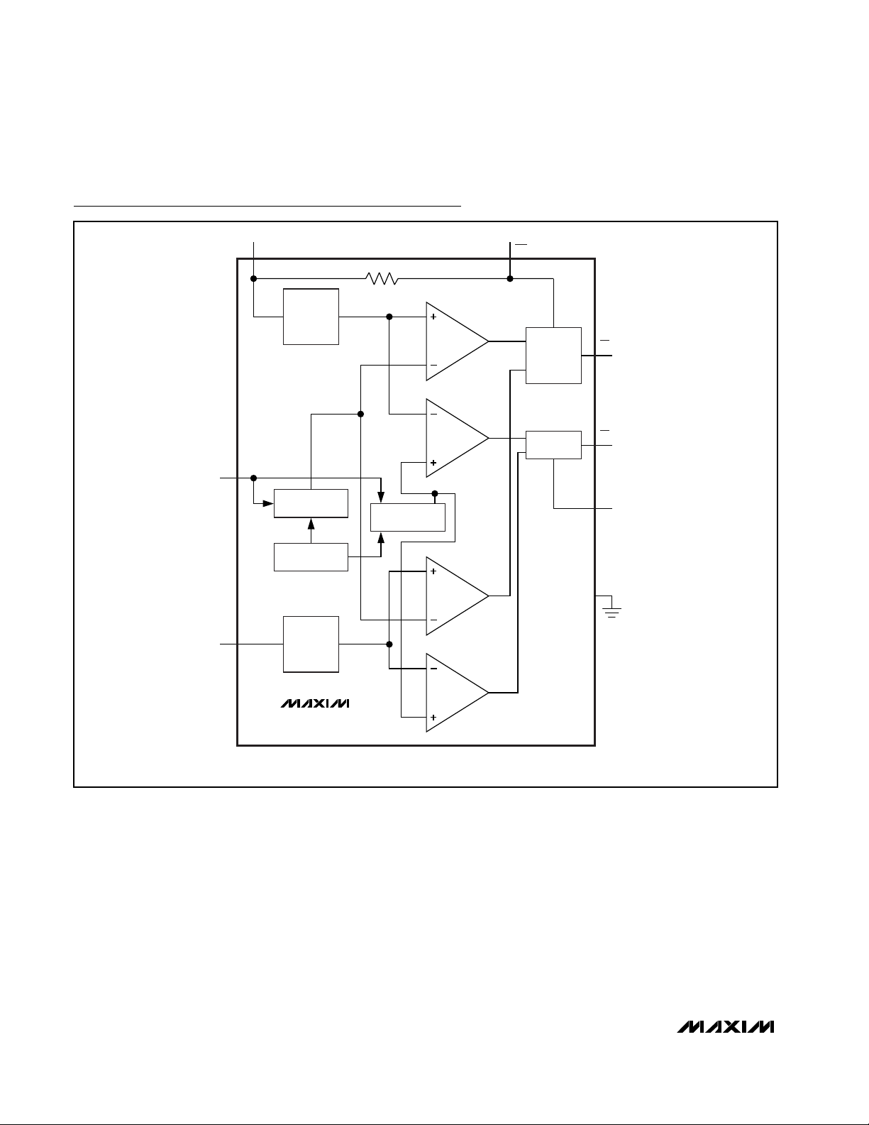
Functional Diagrams
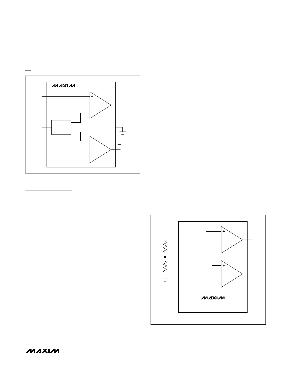
Figure 1. MAX6754/MAX6755/MAX6756 Functional Diagram
PIN
MAX6754/
MAX6755/
MAX6756
MAX6757/
MAX6758/
MAX6759
MAX6760/
MAX6761/
MAX6762
MAX6763/
MAX6764
7 — OVLATCH
——— 3 UVIN
——— 4 UV
——— 6 OVIN
——EP — EP
NAME FUNCTION
Overvoltage Output Latch Control Input. Drive OVLATCH high to latch
the overvoltage output for any V
OVLATCH low to clear the latch after overvoltage conditions have been
removed. The latch is transparent when OVLATCH is connected to
GND. OVLATCH is a high-impedance input. Use external pullup or
pulldown.
Undervoltage Input. UV is low when UVIN is below the internal 0.5V
threshold. UV is high when UVIN is above the internal 0.5V threshold.
Undervoltage Output. UV is low when UVIN is below the internal 0.5V
threshold. UV is high when UVIN is above the internal 0.5V threshold.
There is no timeout delay period for the UV output.
Overvoltage Input. OV is low when OVIN is above the internal 0.5V
threshold. OV is high when OVIN is below the internal 0.5V threshold.
Exposed Pad. EP is internally connected to GND. Leave EP
unconnected or connect to GND.
V
CC
or V
CC
CC2
overvoltage condition. Drive
MR
ADJUST
SET
MONITOR
VOLTAGE
UV THRESHOLD
-5%, -10%, -15%
INTERNAL
REFERENCE
UV
OV
OV THRESHOLD
+5%, +10%, +15%
TH
UV MONITOR
TH
OV MONITOR
MAX6754/MAX6755/MAX6756
TIMEOUT
PERIOD
OPTION
( ) MAX6755 ONLY.
(RESET)/
RESET
GND
Page 11

MAX6754–MAX6764
Low-Power, Single/Dual-Voltage Window
Detectors
______________________________________________________________________________________ 11
Figure 2. MAX6757/MAX6758/MAX6759 Functional Diagram
Functional Diagrams (continued)
SET
V
CC
ADJUST
MONITOR
VOLTAGE
UV THRESHOLD
-5%, -10%, -15%
INTERNAL
REFERENCE
UV
OV
OV THRESHOLD
+5%, +10%, +15%
(UV)/
UV
MR
OV
GND
TH
UV MONITOR
V
CC
TH
OV MONITOR
MAX6757/MAX6758/MAX6759
TIMEOUT
PERIOD
OPTION
( ) MAX6758 ONLY.
Page 12
MAX6754–MAX6764
Low-Power, Single/Dual-Voltage Window
Detectors
12 ______________________________________________________________________________________
Figure 3. MAX6760/MAX6761/MAX6762 Functional Diagram
Functional Diagrams (continued)
CC
ADJUST
MONITOR
VOLTAGE
SET
V
CC2
UV THRESHOLD
-5%, -10%, -15%
INTERNAL
REFERENCE
ADJUST
MONITOR
VOLTAGE
UV
TH
OV
TH
OV THRESHOLD
+5%, +10%, +15%
UV
TH
UV MONITOR
OV MONITOR
UV MONITOR
MRV
TIMEOUT
PERIOD
OPTION
OV
CIRCUIT
(UV)/
UV
OV
OVLATCH
GND
OV
MAX6760/MAX6761/MAX6762
TH
OV MONITOR
( ) MAX6761 ONLY.
Page 13
MAX6754–MAX6764
Low-Power, Single/Dual-Voltage Window
Detectors
______________________________________________________________________________________ 13
Detailed Description
The MAX6754–MAX6764 are low-power window voltage detectors capable of monitoring undervoltage and
overvoltage conditions on system power supplies.
Whenever a monitored voltage falls below its undervoltage threshold or exceeds its overvoltage threshold,
these devices assert their outputs to notify the system
(see Functional Diagrams).
The MAX6754/MAX6755/MAX6756 are single-voltage
window detectors with internally fixed nominal voltage,
externally adjustable set window, single reset
under/overvoltage output, and a manual reset input.
The MAX6757/MAX6758/MAX6759 are single-voltage
window detectors with internally set nominal voltage,
externally adjustable set window, separate under/overvoltage outputs, and manual reset input.
The MAX6760/MAX6761/MAX6762 are dual-voltage
window detectors with internally/externally set nominal
voltages, externally adjustable set window, separate
under/overvoltage outputs, manual reset input, and
overvoltage latch functions.
The MAX6763/MAX6764 are single adjustable window
detectors with separate under/overvoltage outputs.
The MAX6754–MAX6762 offer factory-fixed voltage
thresholds for monitoring system voltages from 0.9V to
5V. The MAX6754–MAX6762 include a SET function to
select the window voltage to ±5%, ±10%, or ±15%. The
MAX6763/MAX6764 allow for externally adjustable
upper and lower voltage thresholds to be set externally
(down to 0.5V). The MAX6754–MAX6762 are available
with two timing options (20µs propagation delay or
100ms minimum reset timeout).
Supply Voltages
VCCis the power-supply input and the monitored voltage
of the MAX6754–MAX6762. These devices feature a factory-trimmed VCCand V
CC2
divider that sets the nominal
input range (see Tables 1 and 2). VCCfor the MAX6763/
MAX6764 is the power supply of the device and not the
monitored voltage. For noisy systems, bypass VCCand
V
CC2
each with a 0.1µF capacitor to GND.
Setting the Adjustable Nominal Voltage
Threshold
The MAX6760/MAX6761/MAX6762 (versions with suffixes LA, TA, RA, ZA, WA, and AA) offer adjustable nominal
voltage threshold to monitor V
CC2
. Use an external volt-
age-divider to set the voltage at V
CC2
to 0.4255V.
Configure SET to select a monitor window of ±5%,
±10%, or ±15% (see Figure 5). The MAX6760/MAX6761/
MAX6762 suffix AA monitor only V
CC2
and do not moni-
tor V
CC
.
Figure 4. MAX6763/MAX6764 Functional Diagram
Functional Diagrams (continued)
Figure 5. Setting the Threshold Voltage of V
CC2
MAX6763/MAX6764
UVIN
UV
UV
TH
V
OVIN
INTERNAL
CC
REFERENCE
0.5V
OV
TH
UV MONITOR
GND
OV
OV MONITOR
0.4255V +5%
V+
R1
V
CC2
R2
+10%
+15%
0.4255V -5%
-10%
-15%
MAX6760/MAX6761/MAX6762
(SUFFIXES LA, TA, RA, ZA, WA, AA)
( ) MAX6761 ONLY.
OV
(UV)
UV
Page 14

MAX6754–MAX6764
Low-Power, Single/Dual-Voltage Window
Detectors
14 ______________________________________________________________________________________
Choose R2 to have a resistance of up to 500kΩ.
Calculate R1 by:
R1 = ((V+- 0.4255V) x R2) / 0.4255V
The MAX6763/MAX6764 provide inputs to a window
detector allowing the programming of the threshold
voltage to within VCC(see Figure 6).
Choose R1, R2, and R3 such that:
(V+ / (R1 + R2 + R3)) ≥ 1µA
SET
The MAX6754–MAX6762 allow the setting of the window
voltage range of the voltage detector. Connect SET to
GND to set a ±5% window. Connect SET to V
CC
for a
±10% window. Bias SET to VCC/2 for a ±15% window.
Manual Reset (MR)
The MAX6754–MAX6762 include an active-low manual
reset input. Drive MR low to assert a reset output
(MAX6754/MAX6755/MAX6756) or an undervoltage
output (MAX6757/MAX6758/MAX6759). The output
remains asserted for the specified propagation delay
time (see Figure 7) after MR goes high. MR is internally
pulled to VCCwith a 26kΩ resistor.
Overvoltage Latch Control Input
(OVLATCH)
The MAX6760/MAX6761/MAX6762 provide an overvoltage latch control input (OVLATCH). Drive OVLATCH
high to latch the overvoltage output for any VCCor
V
CC2
overvoltage condition. Drive OVLATCH low to
clear the latch after overvoltage conditions have been
removed. The latch is transparent when OVLATCH is
connected to GND. OVLATCH is a high impedance
input. Use external pullup or pulldown.
Reset, Undervoltage, and Overvoltage
Outputs (RESET,
RESET, UV
, UV, OV)
RESET, RESET, UV, UV, and OV outputs assert when
the monitored supply is below the selected UV
TH
threshold or above the selected OVTHthreshold. The
reset output deasserts after the specified timeout period when the monitored supply rises above the UV
TH
threshold or drops below the OVTHthreshold. The
push-pull versions are referenced to VCC.
The MAX6760/MAX6761/MAX6762 monitor both V
CC
and V
CC2
. An under/overvoltage condition on either
voltage supply asserts the corresponding output.
RESET and UV are guaranteed to be in the correct
logic state when V
CC
or V
CC2
> 1V.
Figure 6. Setting the Under/Overvoltage Window
Figure 7a. Manual Reset/
Reset
Timing Diagram
Figure 7b. VCC/RESET, UVTiming Diagram
V+
R1
MAX6763/MAX6764
UVIN
UV
UV
TH
INTERNAL
V
CC
R2
R3
REFERENCE
0.5V
OVIN
OVERVOLTAGE ASSERTS WHEN
UNDERVOLTAGE ASSERTS WHEN
OV
TH
UV MONITOR
OV MONITOR
V+ x R3
R1 + R2 + R3
V+ x (R2 + R3)
R1 + R2 + R3
GND
OV
> 0.5V
< 0.5V
MR
RESET, UV
V
CC
t
D-UV
RESET, UV
(RESET IS THE COMPLEMENT OF RESET)
t
D-MR
t
MR_P
t
RP
Page 15

MAX6754–MAX6764
Low-Power, Single/Dual-Voltage Window
Detectors
______________________________________________________________________________________ 15
Applications Information
Microprocessor Monitoring
Figure 8 shows a microprocessor monitoring circuit. An
overvoltage condition on either the core or I/O supply
turns the SCR on, blowing the fuse to disconnect the
circuit from the power source. An optional capacitor
(C1) on the gate of the SCR provides additional transient immunity against nuisance trips.
Figure 8. Microprocessor Monitoring
Selector Guide
CORE
DC-DC
CONVERTER
UNREGULATED
POWER SOURCE
FUSE
SCR
I/O
DC-DC
CONVERTER
100kΩ 100kΩ
100kΩ
CORE
I/O
µP
MAX6760
V
V
GND
SET
CC2
CC
OVLATCH
MR
PUSH BUTTON
UV
OV
RESET
NMI
*C1
1µF
PUSH-PULL
RESET
PUSH-PULL
RESET
OPEN-DRAIN
MAX6754 X —
MAX6755 — X
MAX6756 ——
MAX6757 ——
MAX6758 ——
MAX6759 ——
MAX6760 ——
MAX6761 ——
MAX6762 ——
MAX6763 ——
MAX6764 ——
RESET
—
—
X
—
—
—
—
—
—
—
—
*OPTIONAL.
PUSH-PULLUVPUSH-PULLUVOPEN-DRAINUVPUSH-PULLOVOPEN-DRAIN
OV
——
——
——
X —
— X
——
X —
— X
——
X —
— X
—
—
—
—
—
—
—
—
—
——
——
—
— X
— X
X
— X
— X
— X
X
— X
X —
— X
Page 16

MAX6754–MAX6764
Low-Power, Single/Dual-Voltage Window
Detectors
16 ______________________________________________________________________________________
Ordering Information (continued)
*Note: Insert the threshold level suffixes for VCCand V
CC2
(Tables 1 and 2) after UK, UT, or TA. For the
MAX6754–MAX6759, insert only the V
CC
threshold suffix after
the UK or UT. Insert the reset timeout delay (Table 3) after D to
complete the part number. For example, the MAX6760TALTD3-T
provides a V
CC
threshold of 5V, a V
CC2
threshold of 3.3V, and a
100ms minimum reset timeout period. Sample stock is generally
held on standard versions only (see the Standard Versions
table). Standard versions have an order increment requirement
of 2500 pieces. Nonstandard versions have an order increment
requirement of 10,000 pieces. Contact factory for availability.
Table 1. Window Threshold Voltage
Suffix Guide Single Fixed V
CC
(MAX6754—MAX6759)
Table 2. Window Threshold Voltage
Suffix Guide Dual Fixed/Adjustable
(MAX6760/MAX6761/MAX6762)
*See Setting the Adjustable Nominal Voltage Threshold Section.
Table 3. Timeout Period Suffix Guide
**Future product—contact factory for availability.
PART NO. SUFFIX VCC NOMINAL SYSTEM VOLTAGE (V)
L 5.0
T 3.3
R 3.0
Z 2.5
W 1.8
PART NO.
SUFFIX
LT 5 3.3
LR 5 3.0
LA 5 ADJ*
TZ 3.3 2.5
TW 3.3 1.8
TI 3.3 1.5
TG 3.3 1.2
TE 3.3 0.9
TA 3.3 ADJ*
RZ 3.0 2.5
RW 3.0 1.8
RI 3.0 1.5
RG 3.0 1.2
RE 3.0 0.9
RA 3.0 ADJ*
ZW 2.5 1.8
ZI 2.5 1.5
ZG 2.5 1.2
ZE 2.5 0.9
ZA 2.5 ADJ*
WI 1.8 1.5
WG 1.8 1.2
WE 1.8 0.9
WA 1.8 ADJ*
AA – ADJ*
V
NOMINAL
CC
SYSTEM VOLTAGE
(V)
V
NOMINAL
CC2
SYSTEM VOLTAGE
(V)
TIMEOUT
PERIOD SUFFIX
D0 — 0.02 —
D3 100 185 320
PART* TEMP RANGE PIN-PACKAGE
MAX6759UT_D_-T -40°C to +125°C 6 SOT23-6
MAX6760TA_ _D_-T -40°C to +125°C 8 TDFN-8
MAX6761TA_ _D_-T -40°C to +125°C 8 TDFN-8
MAX6762TA_ _D_-T -40°C to +125°C 8 TDFN-8
MAX6763UT-T** -40°C to +125°C 6 SOT23-6
MAX6764UT-T** -40°C to +125°C 6 SOT23-6
ACTIVE TIMEOUT PERIOD
MIN (ms) TYP (MS) MAX (ms)
Page 17

MAX6754–MAX6764
Low-Power, Single/Dual-Voltage Window
Detectors
______________________________________________________________________________________ 17
Standard Versions Table
PART TOP MARK
MAX6754UKLD0 AEOC
MAX6754UKLD3 AEJN
MAX6754UKTD0 AEOD
MAX6754UKTD3 AEJO
MAX6754UKZD0 AEJQ
MAX6754UKZD3 AEOF
MAX6754UKWD0 AEOG
MAX6754UKWD3 AEJR
MAX6755UKLD0 AEOH
MAX6755UKLD3 AEJS
MAX6755UKTD0 AEOI
MAX6755UKTD3 AEJT
MAX6755UKZD0 AEKV
MAX6755UKZD3 AEOK
MAX6755UKWD0 AEOL
MAX6755UKWD3 AEJW
MAX6756UKLD0 AEJX
MAX6756UKLD3 AEOM
MAX6756UKTD0 AEJY
MAX6756UKTD3 AEON
MAX6756UKZD0 AEOP
MAX6756UKZD3 AEKA
MAX6756UKWD0 AEKB
MAX6756UKWD3 AEOQ
MAX6757UTTD0 ABST
MAX6757UTTD3 ABRB
MAX6757UTLD0 ABSO
MAX6757UTLD3 ABRC
MAX6757UTZD0 ABRE
MAX6757UTZD3 ABSW
MAX6757UTWD0 ABSX
MAX6757UTWD3 ABRF
PART TOP MARK
MAX6758UTLD0 ABSY
MAX6758UTLD3 ABRG
MAX6758UTTD0 ABSZ
MAX6758UTTD3 ABRH
MAX6758UTZD0 ABRJ
MAX6758UTZD3 ABTB
MAX6758UTWD0 ABTC
MAX6758UTWD3 ABRK
MAX6759UTLD0 ABRL
MAX6759UTLD3 ABTD
MAX6759UTTD0 ABRM
MAX6759UTTD3 ABTE
MAX6759UTZD0 ABTG
MAX6759UTZD3 ABRO
MAX6759UTWD0 ABRP
MAX6759UTWD3 ABTH
MAX6760TALTD3 AIO
MAX6760TALAD3 AHI
MAX6760TATZD3 AIR
MAX6760TATWD3 AHJ
MAX6760TATAD3 AIT
MAX6760TARAD3 AIV
MAX6760TAZWD3 AIX
MAX6760TAZAD3 AIZ
MAX6760TAWED3 AJB
MAX6760TAWAD3 AHL
Page 18

MAX6754–MAX6764
Low-Power, Single/Dual-Voltage Window
Detectors
18 ______________________________________________________________________________________
Standard Versions Table (continued)
PART TOP MARK
MAX6761TALTD3 AJD
MAX6761TALAD3 AHN
MAX6761TATZD3 AJG
MAX6761TATWD3 AHO
MAX6761TATAD3 AJI
MAX6761TARAD3 AJK
MAX6761TAZWD3 AJM
MAX6761TAZAD3 AJO
MAX6761TAWED3 AJQ
MAX6761TAWAD3 AHQ
MAX6762TALTD3 AJT
MAX6762TALAD3 AHR
MAX6762TATZD3 AJW
MAX6762TATWD3 AJY
MAX6762TATAD3 AKA
MAX6762TARAD3 AKB
MAX6762TAZWD3 AHT
MAX6762TAZAD3 AKE
MAX6762TAWED3 AKF
MAX6762TAWAD3 AKH
MAX6763UTAD3 ABRQ
MAX6764UTAD3 ABRR
PART TOP MARK
Page 19

MAX6754–MAX6764
Low-Power, Single/Dual-Voltage Window
Detectors
______________________________________________________________________________________ 19
Chip Information
TRANSISTOR COUNT: 726
PROCESS: BiCMOS
GND
RESET (RESET)MR
1 5 SETV
CC
MAX6754
MAX6755
MAX6756
SOT23
( ) MAX6755 ONLY.
TOP VIEW
2
34
GND
UV (UV)
1 6 SET
5OV
V
CC
MAX6757
MAX6758
MAX6759
SOT23
( ) MAX6758 ONLY.
2
34
MR
1
2
3
4
8
7
6
5
MR
OVLATCH
UV (UV)
OV
SET
V
CC2
GND
V
CC
MAX6760
MAX6761
MAX6762
TDFN
( ) MAX6761 ONLY.
GND
UV
1 6 OVIN
5OV
V
CC
MAX6763
MAX6764
SOT23
2
34
UVIN
Pin Configurations
Page 20

MAX6754–MAX6764
Low-Power, Single/Dual-Voltage Window
Detectors
20 ______________________________________________________________________________________
Package Information
(The package drawing(s) in this data sheet may not reflect the most current specifications. For the latest package outline information,
go to www.maxim-ic.com/packages.)
D
PIN 1
INDEX
AREA
A
NUMBER OF LEADS SHOWN ARE FOR REFERENCE ONLY
COMMON DIMENSIONS
MIN. MAX.
SYMBOL
0.70 0.80
A
2.90 3.10
D
2.90 3.10
E
0.00 0.05
A1
L
0.20 0.40
k
0.25 MIN.
A2 0.20 REF.
A
A2
b
E
A1
DETAIL A
L
E2
e
C
L
e
D2
C0.35
C
L
e
DALLAS
SEMICONDUCTOR
PROPRIETARY INFORMATION
TITLE:
PACKAGE OUTLINE, 6, 8 & 10L,
TDFN, EXPOSED PAD, 3x3x0.80 mm
APPROVAL
DOCUMENT CONTROL NO. REV.
L
PIN 1 ID
1N1
[(N/2)-1] x e
REF.
k
L
21-0137 D
6, 8, &10L, DFN THIN.EPS
1
2
PACKAGE VARIATIONS
PKG. CODE
T633-1 1.50–0.10D22.30–0.10
N
6
1.50–0.10
E2
2.30–0.10T833-1 8
JEDEC SPEC
0.95 BSCeMO229 / WEEA
MO229 / WEEC
0.65 BSC
[(N/2)-1] x e
0.40–0.05b1.90 REF
1.95 REF0.30–0.05
0.25–0.05 2.00 REFMO229 / WEED-30.50 BSC1.50–0.10 2.30–0.1010T1033-1
DALLAS
SEMICONDUCTOR
PROPRIETARY INFORMATION
TITLE:
PACKAGE OUTLINE, 6, 8 & 10L,
TDFN, EXPOSED PAD, 3x3x0.80 mm
DOCUMENT CONTROL NO.APPROVAL
21-0137
REV.
2
2
D
Page 21

MAX6754–MAX6764
Low-Power, Single/Dual-Voltage Window
Detectors
______________________________________________________________________________________ 21
Package Information (continued)
(The package drawing(s) in this data sheet may not reflect the most current specifications. For the latest package outline information,
go to www.maxim-ic.com/packages.)
SOT-23 5L .EPS
PACKAGE OUTLINE, SOT-23, 5L
1
21-0057
E
1
Page 22

MAX6754–MAX6764
Low-Power, Single/Dual-Voltage Window
Detectors
Maxim cannot assume responsibility for use of any circuitry other than circuitry entirely embodied in a Maxim product. No circuit patent licenses are
implied. Maxim reserves the right to change the circuitry and specifications without notice at any time.
22 ____________________Maxim Integrated Products, 120 San Gabriel Drive, Sunnyvale, CA 94086 408-737-7600
© 2003 Maxim Integrated Products Printed USA is a registered trademark of Maxim Integrated Products.
Package Information (continued)
(The package drawing(s) in this data sheet may not reflect the most current specifications. For the latest package outline information,
go to www.maxim-ic.com/packages.)
6LSOT.EPS
PACKAGE OUTLINE, SOT-23, 6L
1
21-0058
F
1
 Loading...