

Page 1
General Description
The MAX6695/MAX6696 are precise, dual-remote, and
local digital temperature sensors. They accurately measure the temperature of their own die and two remote
diode-connected transistors, and report the temperature in digital form on a 2-wire serial interface. The
remote diode is typically the emitter-base junction of a
common-collector PNP on a CPU, FPGA, GPU, or ASIC.
The 2-wire serial interface accepts standard system
management bus (SMBus™) commands such as Write
Byte, Read Byte, Send Byte, and Receive Byte to read
the temperature data and program the alarm thresholds
and conversion rate. The MAX6695/MAX6696 can function autonomously with a programmable conversion
rate, which allows control of supply current and temperature update rate to match system needs. For conversion rates of 2Hz or less, the temperature is
represented as 10 bits + sign with a resolution of
+0.125°C. When the conversion rate is 4Hz, output data
is 7 bits + sign with a resolution of +1°C. The MAX6695/
MAX6696 also include an SMBus timeout feature to
enhance system reliability.
Remote temperature sensing accuracy is ±1.5°C between +60°C and +100°C with no calibration needed.
The MAX6695/MAX6696 measure temperatures from
-40°C to +125°C. In addition to the SMBus ALERT out-
put, the MAX6695/MAX6696 feature two overtemperature limit indicators (OT1 and OT2), which are active
only while the temperature is above the corresponding
programmable temperature limits. The OT1 and OT2
outputs are typically used for fan control, clock throttling, or system shutdown.
The MAX6695 has a fixed SMBus address. The
MAX6696 has nine different pin-selectable SMBus
addresses. The MAX6695 is available in a 10-pin
µMAX®and the MAX6696 is available in a 16-pin QSOP
package. Both operate throughout the -40°C to +125°C
temperature range.
Applications
Notebook Computers
Desktop Computers
Servers
Workstations
Test and Measurement Equipment
Features
♦ Measure One Local and Two Remote
Temperatures
♦ 11-Bit, 0.125°C Resolution
♦ High Accuracy ±1.5°C (max) from +60°C to +100°C
(Remote)
♦ ACPI Compliant
♦ Programmable Under/Overtemperature Alarms
♦ Programmable Conversion Rate
♦ Three Alarm Outputs: ALERT, OT1, and OT2
♦ SMBus/I2C™-Compatible Interface
MAX6695/MAX6696
Dual Remote/Local Temperature Sensors with
SMBus Serial Interface
________________________________________________________________ Maxim Integrated Products 1
Ordering Information
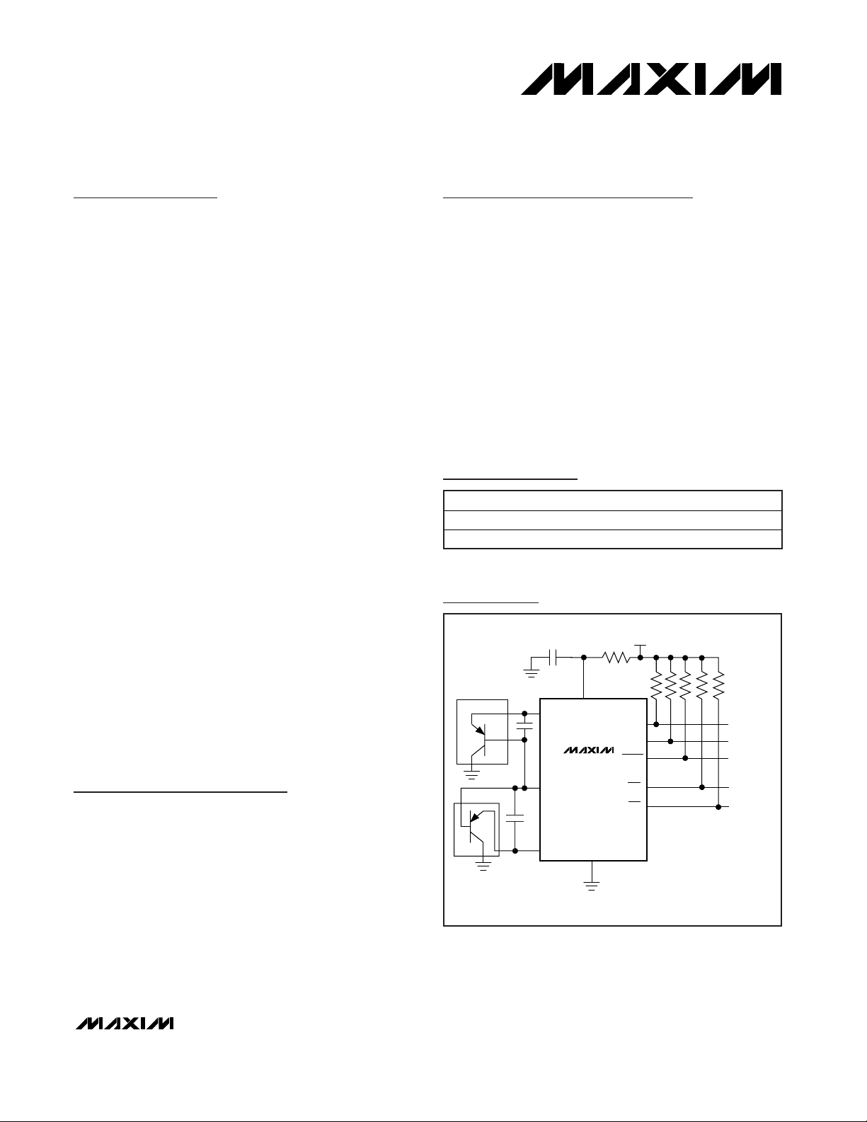
Typical Operating Circuit
19-3183; Rev 1; 5/04
For pricing, delivery, and ordering information, please contact Maxim/Dallas Direct! at
1-888-629-4642, or visit Maxim’s website at www.maxim-ic.com.
PART TEMP RANGE PIN-PACKAGE
MAX6695AUB
10 µMAX
MAX6696AEE
16 QSOP
SMBus is a trademark of Intel Corp.
Pin Configurations appear at end of data sheet.
CLOCK
DATA
TO SYSTEM
SHUTDOWN
GND
OT2
SMBCLK
OT1
SMBDATA
V
CC
INTERRUPT
TO µP
0.1µF
DXN
DXP1
47Ω
10kΩ
EACH
ALERT
+3.3V
MAX6695
CPU
TO CLOCK
THROTTLING
DXP2
GRAPHICS
PROCESSOR
Typical Operating Circuits continued at end of data sheet.
I2C is a trademark of Philips Corp. Purchase of I2C components
from Maxim Integrated Products, Inc., or one of its sublicensed
Associated Companies, conveys a license under the Philips
I
2
C Patent Rights to use these components in an I2C system,
provided that the system conforms to the I
2
C Standard
Specification as defined by Philips.
µMAX is a registered trademark of Maxim Integrated Products, Inc.
-40°C to +125°C
-40°C to +125°C
Page 2

MAX6695/MAX6696
Dual Remote/Local Temperature Sensors with
SMBus Serial Interface
2 _______________________________________________________________________________________
ABSOLUTE MAXIMUM RATINGS
Stresses beyond those listed under “Absolute Maximum Ratings” may cause permanent damage to the device. These are stress ratings only, and functional
operation of the device at these or any other conditions beyond those indicated in the operational sections of the specifications is not implied. Exposure to
absolute maximum rating conditions for extended periods may affect device reliability.
VCC...........................................................................-0.3V to +6V
DXP1, DXP2................................................-0.3V to (V
CC
+ 0.3V)
DXN ......................................................................-0.3V to +0.8V
SMBCLK, SMBDATA, ALERT ...................................-0.3V to +6V
RESET, STBY, ADD0, ADD1, OT1, OT2 ...................-0.3V to +6V
SMBDATA Current .................................................1mA to 50mA
DXN Current ......................................................................±1mA
Continuous Power Dissipation (T
A
= +70°C)
10-Pin mMAX (derate 6.9mW/°C above +70°C).......555.6mW
16-Pin QSOP (derate 8.3mW/°C above +70°C) .......666.7mW
Operating Temperature Range .........................-40°C to +125°C
Junction Temperature .....................................................+150°C
Storage Temperature Range ............................-65°C to +150°C
Lead Temperature (soldering, 10s) ................................+300°C
ELECTRICAL CHARACTERISTICS
(VCC= +3.0V to +3.6V, TA= 0°C to +125°C, unless otherwise noted. Typical values are at VCC= +3.3V and TA= +25°C)
PARAMETER
SYMBOL
CONDITIONS
MIN
TYP
MAX
UNITS
Supply Voltage V
CC
3.0 3.6 V
Standby Supply Current SMBus static, ADC in idle state 10 µA
Operating Current Interface inactive, ADC active 0.5 1 mA
Conversion rate = 0.125Hz 35 70
Conversion rate = 1Hz
500Average Operating Current
Conversion rate = 4Hz
µA
TRJ = +25°C to +100°C
(T
A
= +45°C to +85°C)
Remote Temperature Error
(Note 1)
T
RJ
= -40°C to +125°C (TA = -40°C)
°C
TA = +45°C to +85°C
TA = +25°C to +100°C
TA = 0°C to +125°C
Local Temperature Error
T
A
= -40°C to +125°C
°C
Power-On Reset Threshold VCC, falling edge (Note 2) 1.3
1.6 V
POR Threshold Hysteresis
mV
Undervoltage Lockout Threshold
UVLO Falling edge of VCC disables ADC 2.2 2.8
V
Undervoltage Lockout Hysteresis
90 mV
Channel 1 rate ≤4Hz, channel 2 / local rate
≤2Hz (conversion rate register ≤05h)
Conversion Time
Channel 1 rate ≥8Hz, channel 2 / local rate
≥4Hz (conversion rate register ≥06h)
ms
High level 80
120
Remote-Diode Source Current I
RJ
Low level 8 10 12
µA
ALERT, OT1, OT2
Output Low Sink Current VOL = 0.4V 6 mA
Output High Leakage Current VOH = 3.6V 1 µA
INPUT PIN, ADD0, ADD1 (MAX6696)
Logic Input Low Voltage V
IL
0.3 V
Logic Input High Voltage V
IH
2.9 V
250
T
= 0° C to + 125° C ( TA = + 25° C to + 100° C ) -3.0 +3.0
R J
TRJ = -40°C to +125°C (TA = 0°C to +125°C) -5.0 +5.0
-1.5 +1.5
-2.0 +2.0
-3.0 +3.0
-4.5 +4.5
112.5 125 137.5
56.25 62.5 68.75
500 1000
+3.0
+3.0
1.45
500
100
2.95
Page 3

MAX6695/MAX6696
Dual Remote/Local Temperature Sensors with
SMBus Serial Interface
_______________________________________________________________________________________ 3
ELECTRICAL CHARACTERISTICS (continued)
(VCC= +3.0V to +3.6V, TA= 0°C to +125°C, unless otherwise noted. Typical values are at VCC= +3.3V and TA= +25°C)
PARAMETER
SYMBOL
CONDITIONS
MIN
TYP
MAX
UNITS
INPUT PIN, RESET, STBY (MAX6696)
Logic Input Low Voltage V
IL
0.8 V
Logic Input High Voltage V
IH
2.1 V
Input Leakage Current I
LEAK
-1 +1 µA
SMBus INTERFACE (SMBCLK, SMBDATA, STBY)
Logic Input Low Voltage V
IL
0.8 V
Logic Input High Voltage V
IH
2.1 V
Input Leakage Current I
LEAK
VIN = GND or V
CC
±1 µA
Output Low Sink Current I
OL
VOL = 0.6V 6 mA
Input Capacitance C
IN
5pF
SMBus-COMPATIBLE TIMING (Figures 4 and 5) (Note 2)
Serial Clock Frequency f
SCL
10 100 kHz
Bus Free Time Between STOP
and START Condition
t
BUF
4.7 µs
Repeat START Condition Setup
Time
90% of SMBCLK to 90% of SMBDATA 4.7 µs
START Condition Hold Time
10% of SMBDATA to 90% of SMBCLK 4 µs
STOP Condition Setup Time
90% of SMBCLK to 90% of SMBDATA 4 µs
Clock Low Period t
LOW
10% to 10% 4 µs
Clock High Period t
HIGH
90% to 90% 4.7 µs
Data Setup Time
µs
Data Hold Time
µs
SMB Rise Time t
R
1µs
SMB Fall Time t
F
300 ns
SMBus Timeout SMBDATA low period for interface reset 20 30 40 ms
Note 1: Based on diode ideality factor of 1.008.
Note 2: Specifications are guaranteed by design, not production tested.
t
SU:STA
t
HD:STA
t
SU:STO
t
SU:DAT
t
HD:DAT
250
300
Page 4
MAX6695/MAX6696
Dual Remote/Local Temperature Sensors with
SMBus Serial Interface
4 _______________________________________________________________________________________
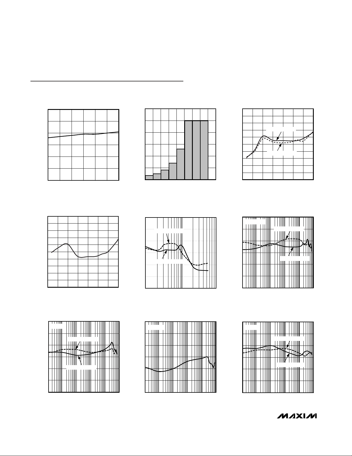
Typical Operating Characteristics
(VCC= 3.3V, TA= +25°C, unless otherwise noted.)
STANDBY SUPPLY CURRENT
vs. SUPPLY VOLTAGE
MAX6695 toc01
SUPPLY VOLTAGE (V)
STANDBY SUPPLY CURRENT (µA)
3.53.43.33.23.1
1
2
3
4
5
6
0
3.0 3.6
AVERAGE OPERATING SUPPLY CURRENT
vs. CONVERSION RATE CONTROL REGISTER VALUE
MAX6695 toc02
CONVERSION RATE CONTROL REGISTER VALUE (hex)
OPERATING SUPPLY CURRENT (µA)
321
100
200
300
400
500
600
0
07654
TEMPERATURE ERROR
vs. REMOTE-DIODE TEMPERATURE
MAX6695 toc03
REMOTE TEMPERATURE (°C)
TEMPERATURE ERROR (°C)
1007525 500-25
-4
-3
-2
-1
0
1
2
3
4
5
-5
-50 125
REMOTE CHANNEL2
REMOTE CHANNEL1
LOCAL TEMPERATURE ERROR
vs. DIE TEMPERATURE
MAX6695 toc04
DIE TEMPERATURE (°C)
TEMPERATURE ERROR (°C)
1007525 500-25
-4
-3
-2
-1
0
1
2
3
4
5
-5
-50 125
TEMPERATURE ERROR
vs. DXP-DXN CAPACITANCE
MAX6695 toc05
DXP-DXN CAPACITANCE (nF)
TEMPERATURE ERROR (°C)
3
-3
-2
-1
0
1
2
1 10 100
REMOTE CHANNEL1
REMOTE CHANNEL2
3
0.001 0.01 0.1 1 10 100
2
1
0
-1
-2
-3
TEMPERATURE ERROR
vs. DIFFERENTIAL NOISE FREQUENCY
MAX6695 toc06
FREQUENCY (MHz)
TEMPERATURE ERROR (°C)
REMOTE CHANNEL1
VIN = 10mV
P-P
REMOTE CHANNEL2
3
0.001 0.01 0.1 1 10 100
2
1
0
-2
-1
-3
REMOTE TEMPERATURE ERROR
vs. POWER-SUPPLY NOISE FREQUENCY
MAX6695 toc07a
FREQUENCY (MHz)
TEMPERATURE ERROR (°C)
100mV
P-P
REMOTE CHANNEL2
REMOTE CHANNEL1
3
0.001 0.01 0.1 1 10 100
2
1
-1
0
-2
-3
LOCAL TEMPERATURE ERROR
vs. POWER-SUPPLY NOISE FREQUENCY
MAX6695 toc07b
FREQUENCY (MHz)
TEMPERATURE ERROR (°C)
100mV
P-P
3
0.001 0.01 0.1 1 10 100
2
1
0
-1
-2
-3
TEMPERATURE ERROR
vs. COMMON-MODE NOISE FREQUENCY
MAX6695 toc08
FREQUENCY (Hz)
TEMPERATURE ERROR (°C)
REMOTE CHANNEL1
10mV
P-P
REMOTE CHANNEL2
Page 5

MAX6695/MAX6696
Dual Remote/Local Temperature Sensors with
SMBus Serial Interface
_______________________________________________________________________________________ 5
Pin Description
PIN
MAX6695 MAX6696
NAME FUNCTION
12V
CC
Supply Voltage Input, +3V to +3.6V. Bypass to GND with a 0.1µF capacitor. A
47Ω series resistor is recommended but not required for additional noise
filtering. See Typical Operating Circuit.
2 3 DXP1
Combined Remote-Diode Current Source and A/D Positive Input for RemoteDiode Channel 1. DO NOT LEAVE DXP1 FLOATING; connect DXP1 to DXN if no
remote diode is used. Place a 2200pF capacitor between DXP1 and DXN for
noise filtering.
34DXN
Combined Remote-Diode Current Sink and A/D Negative Input. DXN is internally
biased to one diode drop above ground.
4 5 DXP2
Combined Remote-Diode Current Source and A/D Positive Input for RemoteDiode Channel 2. DO NOT LEAVE DXP2 FLOATING; connect DXP2 to DXN if no
remote diode is used. Place a 2200pF capacitor between DXP2 and DXN for
noise filtering.
510OT1
Overtemperature Active-Low Output, Open Drain. OT1 is asserted low only when
the temperature is above the programmed OT1 threshold.
6 8 GND Ground
7 9 SMBCLK SMBus Serial-Clock Input
811ALERT
SMBus Alert (Interrupt) Active-Low Output, Open-Drain. Asserts when
temperature exceeds user-set limits (high or low temperature) or when a remote
sensor opens. Stays asserted until acknowledged by either reading the status
register or by successfully responding to an alert response address. See the
ALERT Interrupts section.
9 12 SMBDATA SMBus Serial-Data Input/Output, Open Drain
10 13 OT2
Overtemperature Active-Low Output, Open Drain. OT2 is asserted low only when
temperature is above the programmed OT2 threshold.
— 1, 16 N.C. No Connect
— 6 ADD1
SMBus Slave Address Select Input (Table 10). ADD0 and ADD1 are sampled
upon power-up.
— 7 RESET
Reset Input. Drive RESET high to set all registers to their default values (POR
state). Pull RESET low for normal operation.
— 14 ADD0
SMBus Slave Address Select Input (Table 10). ADD0 and ADD1 are sampled
upon power-up.
—15STBY
Hardware Standby Input. Pull STBY low to put the device into standby mode.
All registers’ data are maintained.
Page 6

MAX6695/MAX6696
Detailed Description
The MAX6695/MAX6696 are temperature sensors
designed to work in conjunction with a microprocessor
or other intelligence in temperature monitoring, protection, or control applications. Communication with the
MAX6695/MAX6696 occurs through the SMBus serial
interface and dedicated alert pins. The overtemperature alarms OT1 and OT2 are asserted if the softwareprogrammed temperature thresholds are exceeded.
OT1 and OT2 can be connected to a fan, system shutdown, or other thermal-management circuitry.
The MAX6695/MAX6696 convert temperatures to digital
data continuously at a programmed rate or by selecting
a single conversion. At the highest conversion rate,
temperature conversion results are stored in the “main”
temperature data registers (at addresses 00h and 01h)
as 7-bit + sign data with the LSB equal to 1°C. At slower conversion rates, 3 additional bits are available at
addresses 11h and 10h, providing 0.125°C resolution.
See Tables 2, 3, and 4 for data formats.
ADC and Multiplexer
The MAX6695/MAX6696 averaging ADC (Figure 1) integrates over a 62.5ms or 125ms period (each channel,
typ), depending on the conversion rate (see Electrical
Characteristics table). The use of an averaging ADC
attains excellent noise rejection.
The MAX6695/MAX6696 multiplexer (Figure 1) automatically steers bias currents through the remote and local
diodes. The ADC and associated circuitry measure
each diode’s forward voltages and compute the temperature based on these voltages. If a remote channel
is not used, connect DXP_ to DXN. Do not leave DXP_
and DXN unconnected. When a conversion is initiated,
all channels are converted whether they are used or
not. The DXN input is biased at one VBEabove ground
by an internal diode to set up the ADC inputs for a differential measurement. Resistance in series with the
remote diode causes about +1/2°C error per ohm.
A/D Conversion Sequence
A conversion sequence consists of a local temperature
measurement and two remote temperature measurements. Each time a conversion begins, whether initiated automatically in the free-running autoconvert mode
(RUN/STOP = 0) or by writing a one-shot command, all
three channels are converted, and the results of the
three measurements are available after the end of conversion. Because it is common to require temperature
measurements to be made at a faster rate on one of the
remote channels than on the other two channels, the
conversion sequence is Remote 1, Local, Remote 1,
Remote 2. Therefore, the Remote 1 conversion rate is
double that of the conversion rate for either of the other
two channels.
A BUSY status bit in status register 1 (see Table 7 and
the Status Byte Functions section) shows that the
device is actually performing a new conversion. The
results of the previous conversion sequence are always
available when the ADC is busy.
Remote-Diode Selection
The MAX6695/MAX6696 can directly measure the die
temperature of CPUs and other ICs that have on-board
temperature-sensing diodes (see the Typical Operating
Circuit) or they can measure the temperature of a discrete diode-connected transistor.
Effect of Ideality Factor
The accuracy of the remote temperature measurements
depends on the ideality factor (n) of the remote “diode”
(actually a transistor). The MAX6695/MAX6696 are optimized for n = 1.008. A thermal diode on the substrate of
an IC is normally a PNP with its collector grounded. DXP_
must be connected to the anode (emitter) and DXN must
be connected to the cathode (base) of this PNP.
If a sense transistor with an ideality factor other than
1.008 is used, the output data will be different from the
data obtained with the optimum ideality factor.
Fortunately, the difference is predictable. Assume a
remote-diode sensor designed for a nominal ideality
factor n
NOMINAL
is used to measure the temperature of
a diode with a different ideality factor n1. The measured
temperature TMcan be corrected using:
where temperature is measured in Kelvin and
n
NOMIMAL
for the MAX6695/MAX6696 is 1.008.
As an example, assume you want to use the MAX6695
or MAX6696 with a CPU that has an ideality factor of
1.002. If the diode has no series resistance, the measured data is related to the real temperature as follows:
For a real temperature of +85°C (358.15K), the measured
temperature is +82.87°C (356.02K), an error of -2.13°C.
Effect of Series Resistance
Series resistance (RS) with a sensing diode contributes
additional error. For nominal diode currents of 10µA
TT
n
n
TT
ACTUAL M
NOMINAL
MM
=×
⎛
⎝
⎜
⎞
⎠
⎟
=×
⎛
⎝
⎜
⎞
⎠
⎟
=×
()
1
1 008
1 002
1 00599
.
.
.
TT
n
n
M ACTUAL
NOMINAL
=×
⎛
⎝
⎜
⎞
⎠
⎟
1
Dual Remote/Local Temperature Sensors with
SMBus Serial Interface
6 _______________________________________________________________________________________
Page 7

and 100µA, the change in the measured voltage due to
series resistance is:
Since 1°C corresponds to 198.6µV, series resistance
contributes a temperature offset of:
Assume that the sensing diode being measured has a
series resistance of 3Ω. The series resistance contributes a temperature offset of:
The effects of the ideality factor and series resistance
are additive. If the diode has an ideality factor of 1.002
and series resistance of 3Ω, the total offset can be calculated by adding error due to series resistance with
error due to ideality factor:
1.36°C - 2.13°C = -0.77°C
for a diode temperature of +85°C.
3 0 453 1 36ΩΩ×
°
=+ °. .
C
C
90
198 6
0 453
µµV
V
C
C
Ω
Ω
.
.°=
°
∆VAARAR
MSS
=−×=×()100 10 90µµ µ
MAX6695/MAX6696
Dual Remote/Local Temperature Sensors with
SMBus Serial Interface
_______________________________________________________________________________________ 7
OT2
OT1
ALERT
DXP2
DXN
DXP1
RESET/
UVLO
CIRCUITRY
V
CC
(RESET)
MUX
REMOTE1
REMOTE2
LOCAL
Q
S
R
OT2 THRESHOLDS
ALERT RESPONSE ADDRESS
ALERT THRESHOLD
LOCAL TEMPERATURES
REMOTE TEMPERATURES
COMMAND BYTE
REGISTER BANK
Q
S
R
Q
S
R
ADC
CONTROL
LOGIC
8
8
SMBus
READ
WRITE
(STBY)
SMBDATA
SMBCLK
(ADD0)
(ADD1)
ADDRESS
DECODER
3
DIODE FAULT
() ARE FOR MAX6696 ONLY.
7
OT1 THRESHOLDS
Figure 1. MAX6695/MAX6696 Functional Diagram
Page 8

MAX6695/MAX6696
In this example, the effect of the series resistance and
the ideality factor partially cancel each other.
Discrete Remote Diodes
When the remote-sensing diode is a discrete transistor,
its collector and base must be connected together.
Table 1 lists examples of discrete transistors that are
appropriate for use with the MAX6695/MAX6696.
The transistor must be a small-signal type with a relatively high forward voltage; otherwise, the A/D input
voltage range can be violated. The forward voltage at
the highest expected temperature must be greater than
0.25V at 10µA, and at the lowest expected temperature, the forward voltage must be less than 0.95V at
100µA. Large power transistors must not be used. Also,
ensure that the base resistance is less than 100Ω. Tight
specifications for forward current gain (50 < ß <150, for
example) indicate that the manufacturer has good
process controls and that the devices have consistent
VBEcharacteristics.
Manufacturers of discrete transistors do not normally
specify or guarantee ideality factor. This is normally not
a problem since good-quality discrete transistors tend
to have ideality factors that fall within a relatively narrow
range. We have observed variations in remote temperature readings of less than ±2°C with a variety of discrete transistors. Still, it is good design practice to
verify good consistency of temperature readings with
several discrete transistors from any manufacturer
under consideration.
Thermal Mass and Self-Heating
When sensing local temperature, these temperature
sensors are intended to measure the temperature of the
PC board to which they are soldered. The leads provide a good thermal path between the PC board traces
and the die. As with all IC temperature sensors, thermal
conductivity between the die and the ambient air is
poor by comparison, making air temperature measurements impractical. Because the thermal mass of the PC
board is far greater than that of the MAX6695/
MAX6696, the device follows temperature changes on
the PC board with little or no perceivable delay.
When measuring the temperature of a CPU or other IC
with an on-chip sense junction, thermal mass has virtually no effect; the measured temperature of the junction
tracks the actual temperature within a conversion cycle.
When measuring temperature with discrete remote
transistors, the best thermal response times are
obtained with transistors in small packages (i.e., SOT23
or SC70). Take care to account for thermal gradients
between the heat source and the sensor, and ensure
that stray air currents across the sensor package do
not interfere with measurement accuracy.
Self-heating does not significantly affect measurement
accuracy. Remote-sensor self-heating due to the diode
current source is negligible. For local temperature measurements, the worst-case error occurs when autoconverting at the fastest rate and simultaneously sinking
maximum current at the ALERT output. For example,
with VCC= 3.6V, a 4Hz conversion rate and ALERT
sinking 1mA, the typical power dissipation is:
θ
J-A
for the 16-pin QSOP package is about +120°C/W,
so assuming no copper PC board heat sinking, the
resulting temperature rise is:
Even under these worst-case circumstances, it is difficult to introduce significant self-heating errors.
ADC Noise Filtering
The integrating ADC has good noise rejection for lowfrequency signals such as power-supply hum. In environments with significant high-frequency EMI, connect
an external 2200pF capacitor between DXP_ and DXN.
Larger capacitor values can be used for added filtering, but do not exceed 3300pF because it can introduce errors due to the rise time of the switched current
source. High-frequency noise reduction is needed for
high-accuracy remote measurements. Noise can be
reduced with careful PC board layout as discussed in
the PC Board Layout section.
Low-Power Standby Mode
Standby mode reduces the supply current to less than
10µA by disabling the ADC. Enter hardware standby
(MAX6696 only) by forcing STBY low, or enter software
standby by setting the RUN/STOP bit to 1 in the config-
∆TmW CW C=×°=°2 2 120 0 264./.
VAVmAmW
CC
×+×=500 0 4 1 2 2µ ..
Dual Remote/Local Temperature Sensors with
SMBus Serial Interface
8 _______________________________________________________________________________________
MANUFACTURER MODEL NO.
Central Semiconductor (USA)
CMPT3904
Rohm Semiconductor (USA) SST3904
Samsung (Korea) KST3904-TF
Siemens (Germany) SMBT3904
Zetex (England) FMMT3904CT-ND
Table 1. Remote-Sensor Transistor
Manufacturers
Note: Discrete transistors must be diode connected (base
shorted to collector).
Page 9

uration byte register. Hardware and software standbys
are very similar; all data is retained in memory, and the
SMBus interface is alive and listening for SMBus commands but the SMBus timeout is disabled. The only difference is that in software standby mode, the one-shot
command initiates a conversion. With hardware standby, the one-shot command is ignored. Activity on the
SMBus causes the device to draw extra supply current.
Driving STBY low overrides any software conversion
command. If a hardware or software standby command
is received while a conversion is in progress, the conversion cycle is interrupted, and the temperature registers are not updated. The previous data is not changed
and remains available.
SMBus Digital Interface
From a software perspective, the MAX6695/MAX6696
appear as a series of 8-bit registers that contain temperature data, alarm threshold values, and control bits.
A standard SMBus-compatible 2-wire serial interface is
used to read temperature data and write control bits
and alarm threshold data. The same SMBus slave
address provides access to all functions.
The MAX6695/MAX6696 employ four standard SMBus
protocols: Write Byte, Read Byte, Send Byte, and
Receive Byte (Figure 2). The shorter Receive Byte protocol allows quicker transfers, provided that the correct
data register was previously selected by a Read Byte
instruction. Use caution with the shorter protocols in multimaster systems, since a second master could overwrite
the command byte without informing the first master.
When the conversion rate control register is set ≥ 06h,
temperature data can be read from the read internal
temperature (00h) and read external temperature (01h)
registers. The temperature data format in these registers is 7 bits + sign in two’s-complement form for each
channel, with the LSB representing 1°C (Table 2). The
MSB is transmitted first. Use bit 3 of the configuration
register to select the registers corresponding to remote
1 or remote 2.
When the conversion rate control register is set ≤ 05h,
temperature data can be read from the read internal
temperature (00h) and read external temperature (01h)
registers, the same as for faster conversion rates. An
additional 3 bits can be read from the read external
extended temperature register (10h) and read internal
MAX6695/MAX6696
Dual Remote/Local Temperature Sensors with
SMBus Serial Interface
_______________________________________________________________________________________ 9
Figure 2. SMBus Protocols
ACK
7 bits
ADDRESS ACKWR
8 bits
DATA ACK
1
P
8 bits
S COMMAND
Write Byte Format
Read Byte Format
Send Byte Format Receive Byte Format
Slave Address: equivalent to chip-select line of
a 3-wire interface
Command Byte: selects which
register you are writing to
Data Byte: data goes into the register
set by the command byte (to set
thresholds, configuration masks, and
sampling rate)
ACK
7 bits
ADDRESS ACKWR S ACK
8 bits
DATA
7 bits
ADDRESS RD
8 bits
/// PCOMMAND
Slave Address: equivalent to chip-select line
Command Byte: selects
which register you are
reading from
Slave Address: repeated
due to change in dataflow direction
Data Byte: reads from
the register set by the
command byte
ACK
7 bits
ADDRESS WR
8 bits
COMMAND ACK P ACK
7 bits
ADDRESS RD
8 bits
DATA /// PS
Command Byte: sends command with no data, usually
used for one-shot command
Data Byte: reads data from
the register commanded
by the last Read Byte or
Write Byte transmission;
also used for SMBus Alert
Response return address
S = Start condition Shaded = Slave transmission
P = Stop condition /// = Not acknowledged
Page 10

MAX6695/MAX6696
extended temperature register (11h) (Table 3), which
extends the temperature data to 10 bits + sign and the
resolution to +0.125°C per LSB (Table 4).
When a conversion is complete, the main register and
the extended register are updated almost simultaneously. Ensure that no conversions are completed
between reading the main and extended registers so
that when data that is read, both registers contain the
result of the same conversion.
To ensure valid extended data, read extended resolution temperature data using one of the following
approaches:
• Put the MAX6695/MAX6696 into standby mode by
setting bit 6 of the configuration register to 1. Read
the contents of the data registers. Return to run
mode by setting bit 6 to zero.
• Put the MAX6695/MAX6696 into standby mode by
setting bit 6 of the configuration register to 1. Initiate
a one-shot conversion using Send Byte command
0Fh. When this conversion is complete, read the
contents of the temperature data registers.
Diode Fault Alarm
There is a continuity fault detector at DXP_ that detects
an open circuit between DXP_ and DXN, or a DXP_
short to V
CC
, GND, or DXN. If an open or short circuit
exists, the external temperature register (01h) is loaded
with 1000 0000. Bit 2 (diode fault) of the status registers
is correspondingly set to 1. The ALERT output asserts
for open diode faults but not for shorted diode faults.
Immediately after power-on reset (POR), the status register indicates that no fault is present until the end of
the first conversion. After the conversion is complete,
any diode fault is indicated in the appropriate status
register. Reading the status register clears the diode
fault bit in that register, and clears the ALERT output if
set. If the diode fault is present after the next conversion, the status bit will again be set and the ALERT out-
put will assert if the fault is an open diode fault.
Alarm Threshold Registers
Six registers, WLHO, WLLM, WRHA (1 and 2), and
WRLN (1 and 2), store ALERT threshold values. WLHO
and WLLM, are for internal ALERT high-temperature
and low-temperature limits, respectively. Likewise,
WRHA and WRLN are for external channel 1 and channel 2 high-temperature and low-temperature limits,
respectively (Table 5). If either measured temperature
equals or exceeds the corresponding ALERT threshold
value, the ALERT output is asserted. The POR state of
both internal and external ALERT high-temperature limit
registers is 0100 0110 or +70°C.
Dual Remote/Local Temperature Sensors with
SMBus Serial Interface
10 ______________________________________________________________________________________
TEMP (°C) DIGITAL OUTPUT
+130.00 0 111 1111
+127.00 0 111 1111
+126.00 0 111 1110
+25.25 0 001 1001
+0.50 0 000 0001
0 0 000 0000
-1 1 111 1111
-55 1 100 1001
Diode fault
(short or open)
1 000 0000
Table 2. Data Format (Two’s Complement)
FRACTIONAL
TEMPERATURE (°C)
CONTENTS OF
EXTENDED REGISTER
0 000X XXXX
+0.125 001X XXXX
+0.250 010X XXXX
+0.375 011X XXXX
+0.500 100X XXXX
+0.625 101X XXXX
+0.750 110X XXXX
+0.875 111X XXXX
Table 3. Extended Resolution Register
Note: Extended resolution applies only for conversion rate
control register values of 05h or less.
TEMP (°C)
INTEGER TEMP
FRACTIONAL TEMP
+130.00 0 111 1111 000X XXXX
+127.00 0 111 1111 000X XXXX
+126.5 0 111 1110 100X XXXX
+25.25 0 001 1001 010X XXXX
+0.50 0 000 0000 100X XXXX
0 0 000 0000 000X XXXX
-1 1 111 1111 000X XXXX
-1.25 1111 1111 010X XXXX
-55 1100 1001 000X XXXX
Table 4. Data Format in Extended Mode
Page 11

MAX6695/MAX6696
Dual Remote/Local Temperature Sensors with
SMBus Serial Interface
______________________________________________________________________________________ 11
REGISTER
FUNCTION
RLTS 00 h
0000 0000
(0°C)
Read internal temperature
RRTE 01 h
0000 0000
(0°C)
Read external channel 1 temperature if bit 3 of configuration register is 0;
Read external channel 2 temperature if bit 3 of configuration register is 1
RSL1 02 h 1000 0000 Read status register 1
RCL 03 h 0000 0000 Read configuration byte (fault queue should be disabled at startup)
RCRA 04 h 0000 0110 Read conversion rate byte
RLHN 05 h
0100 0110
(+70°C)
Read internal ALERT high limit
RLLI 06 h
1100 1001
(-55°C)
Read internal ALERT low limit
RRHI 07 h
0100 0110
(+70°C)
Read external channel 1 ALERT high limit if bit 3 of configuration register is 0;
Read external channel 2 ALERT high limit if bit 3 of configuration register is 1
RRLS 08 h
1100 1001
(-55°C)
Read external channel 1 ALERT low limit if bit 3 of configuration register is 0;
Read external channel 2 ALERT low limit if bit 3 of configuration register is 1
WCA 09 h 0010 0000 Write configuration byte
WCRW 0A h 0000 0110 Write conversion rate byte
WLHO 0B h
0100 0110
(+70°C)
Write internal ALERT high limit
WLLM 0C h
1100 1001
(-55°C)
Write internal ALERT low limit
WRHA 0D h
0100 0110
(+70°C)
Write external channel 1 ALERT high limit if bit 3 of configuration register is 0;
Write external channel 2 ALERT high limit if bit 3 of configuration register is 1
WRLN 0E h
1100 1001
(-55°C)
Write external channel 1 ALERT low limit if bit 3 of configuration register is 0;
Write external channel 2 ALERT low limit if bit 3 of configuration register is 1
OSHT 0F h 0000 0000 One shot
REET 10 h 0000 0000
Read extended temp of external channel 1 if bit 3 of configuration register is 0;
Read extended temp of external channel 2 if bit 3 of configuration register is 1
RIET 11 h 0000 0000 Read internal extended temperature
RSL2 12 h 0000 0000 Read status register 2
RWO2E 16 h
0111 1000
(+120°C)
Read/write external OT2 limit for channel 1 if bit 3 of configuration register is 0;
Read/write external OT2 limit for channel 2 if bit 3 of configuration register is 1
RWO2I 17 h
0101 1010
(+90°C)
Read/write internal OT2 limit
RWO1E 19 h
0101 1010
(+90°C)
Read/write external OT1 limit for channel 1 if bit 3 of configuration register is 0;
Read/write external OT1 limit for channel 2 if bit 3 of configuration register is 1
RWO1I 20 h
0100 0110
(+70°C)
Read/write internal OT1 limit
Table 5. Command-Byte Register Bit Assignments
ADDRESS POR STATE
Page 12

MAX6695/MAX6696
The POR state of both internal and external ALERT low-
temperature limit registers is 1100 1001 or -55°C. Use
bit 3 of the configuration register to select remote 1 or
remote 2 when reading or writing remote thresholds.
Additional registers, RWO1E, RWO1I, RWO2E, and
RWO2I, store remote and local alarm threshold data
information corresponding to the OT1 and OT2 outputs
(See the
OT1
and
OT2
Overtemperature Alarms section.)
ALERT
Interrupt Mode
An ALERT interrupt occurs when the internal or external
temperature reading exceeds a high- or low-temperature limit (both limits are user programmable), or when
the remote diode is disconnected (for continuity fault
detection). The ALERT interrupt output signal is latched
and can be cleared only by reading either of the status
registers or by successfully responding to an Alert
Response address. In both cases, the alert is cleared
but is reasserted at the end of the next conversion if the
fault condition still exists. The interrupt does not halt
automatic conversions. The interrupt output pin is open
drain so that multiple devices can share a common
interrupt line. The interrupt rate never exceeds the conversion rate.
Alert Response Address
The SMBus Alert Response interrupt pointer provides
quick fault identification for simple slave devices. Upon
receiving an interrupt signal, the host master can
broadcast a Receive Byte transmission to the Alert
Response slave address (see Slave Addresses section). Then, any slave device that generated an interrupt attempts to identify itself by putting its own
address on the bus.
The Alert Response can activate several different slave
devices simultaneously, similar to the I2C General Call.
If more than one slave attempts to respond, bus arbitration rules apply, and the device with the lower address
code wins. The losing device does not generate an
acknowledgement and continues to hold the ALERT
line low until cleared. (The conditions for clearing an
alert vary depending on the type of slave device.)
Successful completion of the Alert Response protocol
clears the interrupt latch, provided the condition that
caused the alert no longer exists. If the condition still
exists, the device reasserts the ALERT interrupt at the
end of the next conversion.
OT1
and
OT2
Overtemperature Alarms
Two registers, RWO1E and RWO1I, store remote and
local alarm threshold data corresponding to the OT1
output. Two other registers, RWO2E and RWO2I, store
remote and local alarm threshold data corresponding
to the OT2 output. The values stored in these registers
are high-temperature thresholds. The OT1 or OT2 out-
put is asserted if any one of the measured temperatures equals or exceeds the corresponding alarm
threshold value.
OT1 and OT2 always operate in comparator mode and
are asserted when the temperature rises above a value
programmed in the appropriate threshold register. They
are deasserted when the temperature drops below this
threshold, minus the programmed value in the hysteresis HYST register (21h). An overtemperature output can
be used to activate a cooling fan, send a warning, initiate clock throttling, or trigger a system shutdown to
prevent component damage. The HYST byte sets the
amount of hysteresis to deassert both OT1 and OT2
outputs. The data format for the HYST byte is 7 bit +
sign with +1°C resolution. Bit 7 of the HYST register
should always be zero.
OT1 responds immediately to temperature faults. OT2
activates either immediately or after four consecutive remote channel temperature faults, depending on
the state of the fault queue bit (bit 5 of the configuration register).
Command Byte Functions
The 8-bit command byte register (Table 5) is the master
index that points to the various other registers within the
MAX6695/MAX6696. This register’s POR state is 0000
0000, so a Receive Byte transmission (a protocol that
lacks the command byte) occurring immediately after
POR returns the current local temperature data.
One-Shot
The one-shot command immediately forces a new conversion cycle to begin. If the one-shot command is
received when the MAX6695/MAX6696 are in software
standby mode (RUN/STOP bit = 1), a new conversion is
Dual Remote/Local Temperature Sensors with
SMBus Serial Interface
12 ______________________________________________________________________________________
REGISTER
ADDRESS
POR STATE
FUNCTION
HYST 21 h
0000 1010
(10°C)
Temperature hysteresis for OT1 and OT2
RDID FE h 4D h Read manufacturer ID
Table 5. Command-Byte Register Bit Assignments (continued)
Page 13

begun, after which the device returns to standby mode.
If a conversion is in progress when a one-shot command is received, the command is ignored. If a oneshot command is received in autoconvert mode
(RUN/STOP bit = 0) between conversions, a new conversion begins, the conversion rate timer is reset, and
the next automatic conversion takes place after a full
delay elapses.
Fault Queue Function
To avoid false triggering of the MAX6695/MAX6696 in
noisy environments, a fault queue is provided, which
can be enabled by setting bit 5 (configuration register)
to 1. Four channel 1 fault or two channel 2 fault events
must occur consecutively before the fault output (OT2)
becomes active. Any reading that breaks the sequence
resets the fault queue counter. If there are three overlimit readings followed by a within-limit reading, the
remote channel 1 fault queue counter is reset.
Configuration Byte Functions
The configuration byte register (Table 6) is a read-write
register with several functions. Bit 7 is used to mask
(disable) ALERT interrupts. Bit 6 puts the device into
software standby mode (STOP) or autonomous (RUN)
mode. Bit 5, when 1, enables the Fault Queue. Bit 4 is
reserved. Bit 3 is used to select either remote channel 1
or remote channel 2 for reading temperature data or for
setting or reading temperature limits. Bit 2 disables the
SMBus timeout, as well as the Alert Response. Bit 1
masks ALERT interrupt due to channel 2 when high. Bit
0 masks ALERT interrupt due to channel 1 when high.
Status Byte Functions
The status registers (Tables 7 and 8) indicate which (if
any) temperature thresholds have been exceeded and
if there is an open-circuit fault detected with the external sense junctions. Status register 1 also indicates
whether the ADC is converting. After POR, the normal
state of the registers’ bits is zero (except bit 7 of status
register 1), assuming no alert or overtemperature conditions are present. Bits 0 through 6 of status register 1
and bits 1 through 7 of status register 2 are cleared by
any successful read of the status registers, unless the
fault persists. The ALERT output follows the status flag
bit. Both are cleared when successfully read, but if the
condition still exists, they reassert at the end of the next
conversion.
The bits indicating OT1 and OT2 are cleared only on
reading status even if the fault conditions still exist.
Reading the status byte does not clear the OT1 and
OT2 outputs. One way to eliminate the fault condition is
for the measured temperature to drop below the temperature threshold minus the hysteresis value. Another
way to eliminate the fault condition is by writing new
values for the RWO2E, RWO2I, RWO1E, RWO1I, or
HYST registers so that a fault condition is no longer
present.
When autoconverting, if the T
HIGH
and T
LOW
limits are
close together, it is possible for both high-temp and
low-temp status bits to be set, depending on the
amount of time between Status Read operations. In
these circumstances, it is best not to rely on the status
bits to indicate reversals in long-term temperature
changes. Instead, use a current temperature reading to
establish the trend direction.
MAX6695/MAX6696
Dual Remote/Local Temperature Sensors with
SMBus Serial Interface
______________________________________________________________________________________ 13
BIT NAME
POR
STATE
FUNCTION
7(MSB) MASK1 0 Mask ALERT interrupts when 1.
6 RUN/STOP 0
Standby mode control bit. If 1, immediately stops converting and enters
standby mode. If zero, it converts in either one-shot or timer mode.
5 Fault Queue 0
Fault queue enables when 1. When set to 1, four consecutive faults must occur
before OT2 output is asserted.
4 RFU 0 Reserved.
3 Remote 2 Select 0
0: Read/write remote 1 temperature and set-point values.
1: Read/write remote 2 temperature and set-point values.
2
0 When set to 1, it disables the SMBus timeout, as well as the alert response.
1
0 When set to 1, it masks ALERT interrupt due to channel 2.
0
0 When set to 1, it masks ALERT interrupt due to channel 1.
Table 6. Configuration Byte Functions
SMB Timeout Disable
MASK Alert Channel 2
MASK Alert Channel 1
Page 14

MAX6695/MAX6696
Reset (MAX6696 Only)
The MAX6696’s registers are reset to their power-on
values if RESET is driven high. When reset occurs, all
registers go to their default values, and the SMBus
address pins are sampled.
Conversion Rate Byte
The conversion-rate control register (Table 9) programs
the time interval between conversions in free-running
autonomous mode (RUN/STOP = 0). This variable rate
control can be used to reduce the supply current in
portable-equipment applications. The conversion rate
Dual Remote/Local Temperature Sensors with
SMBus Serial Interface
14 ______________________________________________________________________________________
BIT
FUNCTION
7(MSB)
BUSY 1 A/D is busy converting when 1.
6
0
When 1, internal high-temperature ALERT has tripped, cleared by POR or by reading this status
register. If the fault condition still exists, this bit is set again after the next conversion.
5 LLOW 0
When 1, internal low-temperature ALERT has tripped, cleared by POR or by reading this status
register. If the fault condition still exists, this bit is set again after the next conversion.
4
0
A 1 indicates external junction 1 high-temperature ALERT has tripped, cleared by POR or by
reading this status register. If the fault condition still exists, this bit is set again after the next
conversion.
3
0
A 1 i nd i cates exte r nal j uncti on 1 l ow - tem p er atur e ALE RT has tr i p p ed , cl ear ed b y P OR or b y r ead i ng thi s
status r eg i ster . If the faul t cond i ti on sti l l exi sts, thi s b i t i s set ag ai n after the next conver si on.
2
0
A 1 indicates external diode 1 is open, cleared by POR or by reading this status register. If the
fault condition still exists, this bit is set again after the next conversion.
1
0
A 1 indicates external junction 1 temperature exceeds the OT1 threshold, cleared by reading this
register.
0 IOT1 0
A 1 indicates internal junction temperature exceeds the internal OT1 threshold, cleared by
reading this register.
Table 7. Status Register 1 Bit Assignments
BIT
FUNCTION
7(MSB)
IOT2 0
A 1 indicates internal junction temperature exceeds the internal OT2 threshold, cleared by
reading this register.
6
0
A 1 indicates external junction temperature 2 exceeds the external OT2 threshold, cleared by
reading this register.
5
0
A 1 indicates external junction temperature 1 exceeds the OT2 threshold, cleared by reading this
register.
4
0
A 1 indicates external junction 2 high-temperature ALERT has tripped; cleared by POR or readout
of the status register. If the fault condition still exists, this bit is set again after the next conversion.
3
0
A 1 indicates external junction 2 low-temperature ALERT has tripped; cleared by POR or readout
of the status register. If the fault condition still exists, this bit is set again after the next conversion.
2
0
A 1 indicates external diode 2 open; cleared by POR or readout of the status register. If the fault
condition still exists, this bit is set again after the next conversion.
1
0
A 1 indicates external junction 2 temperature exceeds the OT1 threshold, cleared by reading this
register.
0 RFU 0 Reserved.
Table 8. Status Register 2 Bit Assignments
NAME POR
LHIGH
R1HIGH
R1LOW
1OPEN
R1OT1
NAME POR
R2OT2
R1OT2
R2HIGH
R2LOW
2OPEN
R2OT1
Page 15

byte’s POR state is 06h (4Hz). The MAX6695/MAX6696
use only the 3 LSBs of the control register. The 5 MSBs
are don’t care and should be set to zero. The conversion rate tolerance is ±25% at any rate setting.
Valid A/D conversion results for all channels are available one total conversion time after initiating a conversion, whether conversion is initiated through the
RUN/STOP bit, hardware STBY pin, one-shot command, or initial power-up.
Slave Addresses
The MAX6695 has a fixed address of 0011 000. The
MAX6696 device address can be set to any one of nine
different values at power-up by pin strapping ADD0
and ADD1 so that more than one MAX6695/MAX6696
can reside on the same bus without address conflicts
(Table 10).
The address pin states are checked at POR and RESET
only, and the address data stays latched to reduce quiescent supply current due to the bias current needed for
high-impedance state detection. The MAX6695/
MAX6696 also respond to the SMBus Alert Response
slave address (see the Alert Response Address section).
POR and UVLO
To prevent unreliable power-supply conditions from
corrupting the data in memory and causing erratic
behavior, a POR voltage detector monitors VCCand
clears the memory if VCCfalls below 1.45V (typ; see
Electrical Characteristics). When power is first applied
and VCCrises above 2.0V (typ), the logic blocks begin
operating, although reads and writes at VCClevels
below 3.0V are not recommended.
Power-Up Defaults
• Interrupt latch is cleared.
• Address select pin is sampled.
• ADC begins autoconverting at a 4Hz rate for
channel 2/local and 8Hz for channel 1.
• Command register is set to 00h to facilitate quick
internal Receive Byte queries.
•T
HIGH
and T
LOW
registers are set to default max
and min limits, respectively.
• Hysteresis is set to 10°C.
MAX6695/MAX6696
Dual Remote/Local Temperature Sensors with
SMBus Serial Interface
______________________________________________________________________________________ 15
BIT 3
BIT 1
BIT0
HEX
CONVERSION
RATE (Hz) REMOTE
CHANNEL 2 AND
LOCAL
CONVERSION RATE
(Hz) REMOTE
CHANNEL 1
CONVERSION
PERIOD (s)
REMOTE CHANNEL
2 AND LOCAL
CONVERSION
PERIOD (s)
REMOTE CHANNEL
1
0 0 0 00h 0.0625 0.125 16 8
0 0 1 01h 0.125 0.25 8 4
0 1 0 02h 0.25 0.5 4 2
0 1 1 03h 0.5 1 2 1
1 0 0 04h 1 2 1 0.5
1 0 1 05h 2 4 0.5 0.25
1 1 0 06h 4 8 0.25 0.125
1 1 1 07h 4 8 0.25 0.125
Table 9. Conversion-Rate Control Register (POR = 0110)
ADD0 ADD1 ADDRESS
GND GND 0011 000
GND High-Z 0011 001
GND V
CC
0011 010
High-Z GND 0101 001
High-Z High-Z 0101 010
High-Z V
CC
0101 011
V
CC
GND 1001 100
V
CC
High-Z 1001 101
V
CC
V
CC
1001 110
Table 10. POR Slave Address Decoding
(ADD0 and ADD1)
Note: Extended resolution applies only for conversion rate control register values of 05h or less.
Page 16

MAX6695/MAX6696
PC Board Layout
Follow these guidelines to reduce the measurement
error when measuring remote temperature:
1) Place the MAX6695/MAX6696 as close as is practical to the remote diode. In noisy environments, such
as a computer motherboard, this distance can be
4in to 8in (typ). This length can be increased if the
worst noise sources are avoided. Noise sources
include CRTs, clock generators, memory buses, and
PCI buses.
2) Do not route the DXP-DXN lines next to the deflection coils of a CRT. Also, do not route the traces
across fast digital signals, which can easily introduce +30°C error, even with good filtering.
3) Route the DXP and DXN traces in parallel and in
close proximity to each other. Each parallel pair of
traces (DXP1 and DXN or DXP2 and DXN) should go
to a remote diode. Connect the two DXN traces at
the MAX6695/MAX6696. Route these traces away
from any higher voltage traces, such as +12VDC.
Dual Remote/Local Temperature Sensors with
SMBus Serial Interface
16 ______________________________________________________________________________________
SMBCLK
AB CDEFG HIJ
K
SMBDATA
t
SU:STA
t
HD:STA
t
LOWtHIGH
t
SU:DAT
t
HD:DAT
t
SU:STO
t
BUF
A = START CONDITION
B = MSB OF ADDRESS CLOCKED INTO SLAVE
C = LSB OF ADDRESS CLOCKED INTO SLAVE
D = R/W BIT CLOCKED INTO SLAVE
E = SLAVE PULLS SMBDATA LINE LOW
L
M
F = ACKNOWLEDGE BIT CLOCKED INTO MASTER
G = MSB OF DATA CLOCKED INTO SLAVE
H = LSB OF DATA CLOCKED INTO SLAVE
I = MASTER PULLS DATA LINE LOW
J = ACKNOWLEDGE CLOCKED INTO SLAVE
K = ACKNOWLEDGE CLOCK PULSE
L = STOP CONDITION
M = NEW START CONDITION
Figure 3. SMBus Write Timing Diagram
SMBCLK
AB CDEFG HIJ
K
SMBDATA
t
SU:STA
t
HD:STA
t
LOWtHIGH
t
SU:DAT
t
HD:DAT
t
SU:STO
t
BUF
L
M
A = START CONDITION
B = MSB OF ADDRESS CLOCKED INTO SLAVE
C = LSB OF ADDRESS CLOCKED INTO SLAVE
D = R/W BIT CLOCKED INTO SLAVE
E = SLAVE PULLS SMBDATA LINE LOW
F = ACKNOWLEDGE BIT CLOCKED INTO MASTER
G = MSB OF DATA CLOCKED INTO MASTER
H = LSB OF DATA CLOCKED INTO MASTER
I = MASTER PULLS DATA LINE LOW
J = ACKNOWLEDGE CLOCKED INTO SLAVE
K = ACKNOWLEDGE CLOCK PULSE
L = STOP CONDITION
M = NEW START CONDITION
Figure 4. SMBus Read Timing Diagram
Page 17

Leakage currents from PC board contamination
must be dealt with carefully since a 20MΩ leakage
path from DXP to ground causes about +1°C error.
If high-voltage traces are unavoidable, connect
guard traces to GND on either side of the DXP-DXN
traces (Figure 5).
4) Route through as few vias and crossunders as possible to minimize copper/solder thermocouple
effects.
5) Use wide traces when practical.
6) When the power supply is noisy, add a resistor (up
to 47Ω) in series with VCC(see Typical Operating
Circuit).
Twisted-Pair and Shielded Cables
Use a twisted-pair cable to connect the remote sensor
for remote-sensor distances longer than 8in or in very
noisy environments. Twisted-pair cable lengths can be
between 6ft and 12ft before noise introduces excessive
errors. For longer distances, the best solution is a
shielded twisted pair like that used for audio microphones. For example, Belden #8451 works well for distances up to 100ft in a noisy environment. At the
device, connect the twisted pair to DXP and DXN and
the shield to GND. Leave the shield unconnected at the
remote sensor.
For very long cable runs, the cable’s parasitic capacitance often provides noise filtering, so the 2200pF
capacitor can often be removed or reduced in value.
Cable resistance also affects remote-sensor accuracy.
For every 1Ω of series resistance the error is approximately +1/2°C.
Chip Information
TRANSISTOR COUNT: 22,964
PROCESS: BiCMOS
MAX6695/MAX6696
Dual Remote/Local Temperature Sensors with
SMBus Serial Interface
______________________________________________________________________________________ 17
MINIMUM
10 mils
10 mils
10 mils
10 mils
GND
DXN
DXP
GND
Figure 5. Recommended DXP-DXN PC Traces
Typical Operating Circuits (continued)
CLOCK
DATA
TO SYSTEM
SHUTDOWN
STBY
RESETGNDADD1
OT2
SMBCLK
OT1
SMBDATA
V
CC
INTERRUPT
TO µP
0.1µF
DXN
DXP1
47Ω
10kΩ
EACH
ALERT
+3.3V
ADD0
MAX6696
CPU
2N3906
DXP2
TO CLOCK
THROTTLING
Page 18

MAX6695/MAX6696
Dual Remote/Local Temperature Sensors with
SMBus Serial Interface
18 ______________________________________________________________________________________
1
2
3
4
5
10
9
8
7
6
OT2
SMBDATA
ALERT
SMBCLKDXP2
DXN
DXP1
V
CC
MAX6695
µMAX
TOP VIEW
GNDOT1
16
15
14
13
12
11
10
9
1
2
3
4
5
6
7
8
N.C.
N.C.
STBY
ADD0
OT2
SMBDATA
OT1
SMBCLK
MAX6696
QSOP
V
CC
DXP1
ADD1
DXN
DXP2
RESET
GND
ALERT
Pin Configurations
Page 19

MAX6695/MAX6696
Dual Remote/Local Temperature Sensors with
SMBus Serial Interface
______________________________________________________________________________________ 19
Package Information
(The package drawing(s) in this data sheet may not reflect the most current specifications. For the latest package outline information,
go to www.maxim-ic.com/packages
.)
10LUMAX.EPS
PACKAGE OUTLINE, 10L uMAX/uSOP
1
1
21-0061
I
REV.DOCUMENT CONTROL NO.APPROVAL
PROPRIETARY INFORMATION
TITLE:
TOP VIEW
FRONT VIEW
1
0.498 REF
0.0196 REF
S
6°
SIDE VIEW
α
BOTTOM VIEW
0° 0° 6°
0.037 REF
0.0078
MAX
0.006
0.043
0.118
0.120
0.199
0.0275
0.118
0.0106
0.120
0.0197 BSC
INCHES
1
10
L1
0.0035
0.007
e
c
b
0.187
0.0157
0.114
H
L
E2
DIM
0.116
0.114
0.116
0.002
D2
E1
A1
D1
MIN
-A
0.940 REF
0.500 BSC
0.090
0.177
4.75
2.89
0.40
0.200
0.270
5.05
0.70
3.00
MILLIMETERS
0.05
2.89
2.95
2.95
-
MIN
3.00
3.05
0.15
3.05
MAX
1.10
10
0.6±0.1
0.6±0.1
0 0.50±0.1
H
4X S
e
D2
D1
b
A2
A
E2
E1
L
L1
c
α
GAGE PLANE
A2 0.030 0.037 0.75 0.95
A1
Page 20

MAX6695/MAX6696
Dual Remote/Local Temperature Sensors with
SMBus Serial Interface
Maxim cannot assume responsibility for use of any circuitry other than circuitry entirely embodied in a Maxim product. No circuit patent licenses are
implied. Maxim reserves the right to change the circuitry and specifications without notice at any time.
20 ____________________Maxim Integrated Products, 120 San Gabriel Drive, Sunnyvale, CA 94086 408-737-7600
© 2004 Maxim Integrated Products Printed USA is a registered trademark of Maxim Integrated Products.
Package Information (continued)
(The package drawing(s) in this data sheet may not reflect the most current specifications. For the latest package outline information,
go to www.maxim-ic.com/packages
.)
QSOP.EPS
E
1
1
21-0055
PACKAGE OUTLINE, QSOP .150", .025" LEAD PITCH
 Loading...