

Page 1
General Description
The MAX668/MAX669 constant-frequency, pulse-widthmodulating (PWM), current-mode DC-DC controllers are
designed for a wide range of DC-DC conversion applications including step-up, SEPIC, flyback, and isolatedoutput configurations. Power levels of 20W or more can
be controlled with conversion efficiencies of over 90%.
The 1.8V to 28V input voltage range supports a wide
range of battery and AC-powered inputs. An advanced
BiCMOS design features low operating current (220µA),
adjustable operating frequency (100kHz to 500kHz),
soft-start, and a SYNC input allowing the MAX668/
MAX669 oscillator to be locked to an external clock.
DC-DC conversion efficiency is optimized with a low
100mV current-sense voltage as well as with Maxim’s
proprietary Idle Mode™ control scheme. The controller
operates in PWM mode at medium and heavy loads for
lowest noise and optimum efficiency, then pulses only as
needed (with reduced inductor current) to reduce operating current and maximize efficiency under light loads.
A logic-level shutdown input is also included, reducing
supply current to 3.5µA.
The MAX669, optimized for low input voltages with a
guaranteed start-up voltage of 1.8V, requires bootstrapped operation (IC powered from boosted output). It
supports output voltages up to 28V. The MAX668 operates with inputs as low as 3V and can be connected in
either a bootstrapped or non-bootstrapped (IC powered
from input supply or other source) configuration. When
not bootstrapped, it has no restriction on output voltage.
Both ICs are available in an extremely compact 10-pin
µMAX package.
Features
♦ 1.8V Minimum Start-Up Voltage (MAX669)
♦ Wide Input Voltage Range (1.8V to 28V)
♦ Tiny 10-Pin µMAX Package
♦ Current-Mode PWM and Idle Mode™ Operation
♦ Efficiency over 90%
♦ Adjustable 100kHz to 500kHz Oscillator or
SYNC Input
♦ 220µA Quiescent Current
♦ Logic-Level Shutdown
♦ Soft-Start
Applications
Cellular Telephones
Telecom Hardware
LANs and Network Systems
POS Systems
MAX668/MAX669
1.8V to 28V Input, PWM Step-Up
Controllers in µMAX
________________________________________________________________
Maxim Integrated Products
1
19-4778; Rev 0a; 8/98
PART
MAX668EUB
MAX669EUB
-40°C to +85°C
-40°C to +85°C
TEMP. RANGE PIN-PACKAGE
10 µMAX
10 µMAX
EVALUATION KIT MANUAL
FOLLOWS DATA SHEET
Idle Mode is a trademark of Maxim Integrated Products.
Ordering Information
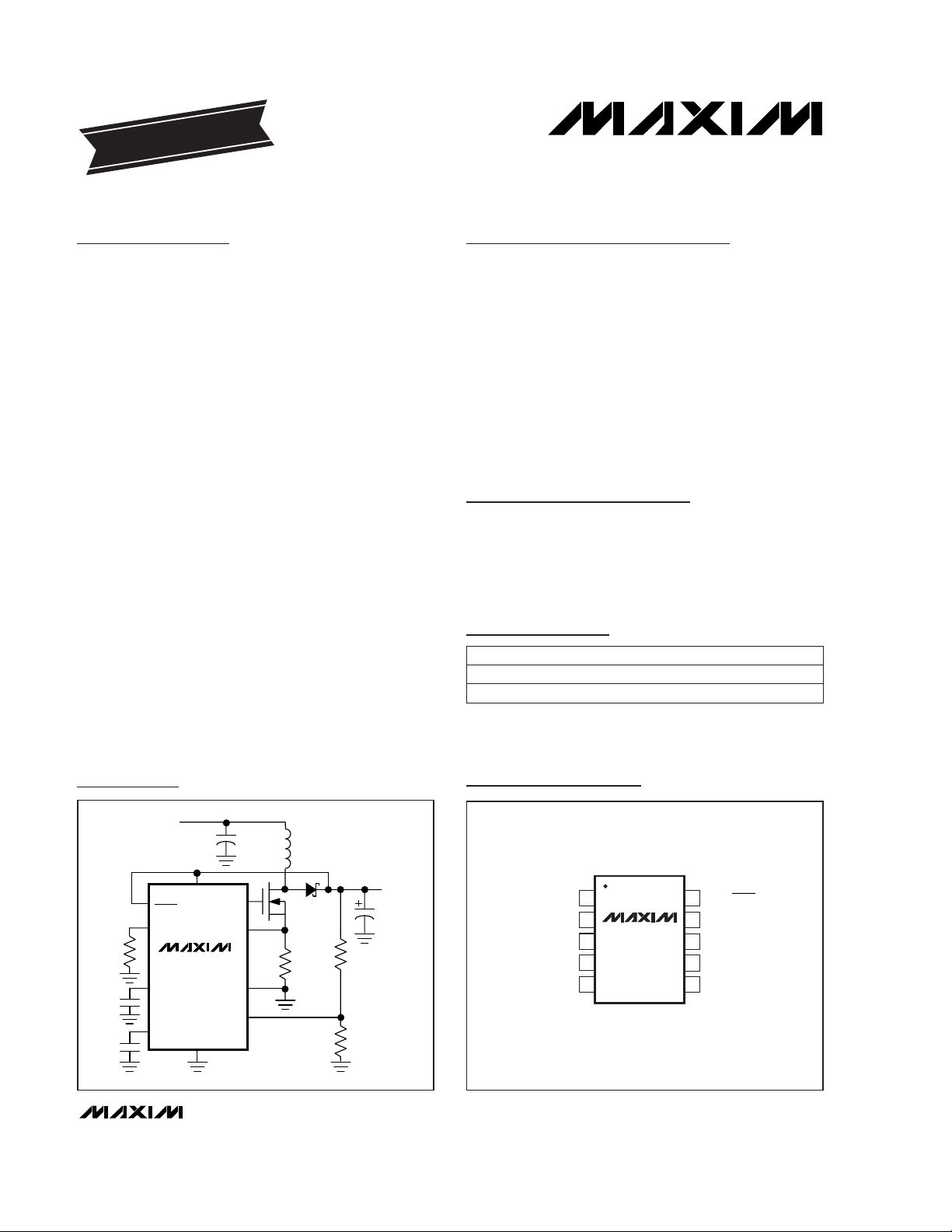
Typical Operating Circuit
MAX669
FREQ
CS+
SYNC/
SHDN
PGND
FB
GND
V
CC
EXT
LDO
REF
V
OUT
= 28V
V
IN
= 1.8V to 28V
1
2
3
4
5
10
9
8
7
6
SYNC/SHDN
V
CC
EXT
PGNDREF
GND
FREQ
LDO
MAX668
MAX669
µMAX
TOP VIEW
CS+FB
Pin Configuration
For free samples & the latest literature: http://www.maxim-ic.com, or phone 1-800-998-8800.
For small orders, phone 1-800-835-8769.
Page 2
MAX668/MAX669
1.8V to 28V Input, PWM Step-Up
Controllers in µMAX
2 _______________________________________________________________________________________
ABSOLUTE MAXIMUM RATINGS
ELECTRICAL CHARACTERISTICS
(VCC= LDO = +5V, R
OSC
= 200kΩ, TA= 0°C to +85°C, unless otherwise noted. Typical values are at TA= +25°C.)
V
CC
to GND ..........................................................-0.3V to +30V
PGND to GND....................................................................±0.3V
SYNC/
SHDN to GND.............................................-0.3V to +30V
EXT, REF to GND.....................................-0.3V to (V
LDO
+ 0.3V)
LDO, FREQ, FB, CS+ to GND ................................ -0.3V to +6V
LDO Output Current...........................................-1mA to +20mA
REF Output Current..............................................-1mA to +1mA
LDO Short Circuit to GND .........................................Momentary
REF Short Circuit to GND..........................................Continuous
Continuous Power Dissipation (T
A
= +70°C)
10-Pin µMAX (derate 5.6mW/°C above +70°C) ..........444mW
Operating Temperature Range ...........................-40°C to +85°C
Junction Temperature......................................................+150°C
Storage Temperature Range .............................-65°C to +150°C
Lead Temperature (soldering,10sec) ..............................+300°C
85 100 115
425 500 575
225 250 275R
OSC
= 200kΩ ±1%
Oscillator Frequency
Oscillator
1.0 1.1 1.2Rising edge, 1% hysteresisREF Undervoltage Lockout Threshold
-2 -10REF load = 0 to 50µA REF Load Regulation
1.225 1.250 1.275No load, C
REF
= 0.22µFREF Output Voltage
2.40 2.50 2.60
Sensed at LDO, falling edge,
hysteresis = 1%, MAX668 only
Undervoltage Lockout Threshold
2.65 5.50
3V ≤ VCC≤ 28V
(includes LDO dropout)
4.50 5.00 5.50
LDO Output Voltage
Reference and LDO Regulators
328MAX668
PWM Controller
Input Voltage Range, V
CC
3.5 6
SYNC/SHDN = GND, VCC= 28V
Shutdown Supply Current (VCC)
220 350VFB= 1.30V, VCC= 3V to 28VVCCSupply Current (Note 1)
0.2 1CS+ forced to GNDCS+ Input Current
51525Idle Mode Current-Sense Threshold
2.7 5.5Input Voltage Range with VCCTied to LDO
1.225 1.250 1.275FB Threshold
1 20 VFB= 1.30VFB Input Current
85 100 115Current Limit Threshold
MIN TYP MAXCONDITIONSPARAMETER
kHz
V
mV
V
V
V
µA
µA
µA
mV
mV
nA
V
V
V
UNITS
MAX669 1.8 28
LDO load =
∞ to 400Ω
5V ≤ VCC≤ 28V
(includes LDO dropout)
R
OSC
= 500kΩ ±1%
R
OSC
= 100kΩ ±1%
0.013
Typically 0.013% per mV on CS+;
VCS+ range is 0 to 100mV for 0 to full
load current.
FB Threshold Load Regulation %/mV
0.012
Typically 0.012% per % duty factor on
EXT; EXT duty factor for a step-up is:
100% (1 – VIN/V
OUT
)
FB Threshold Line Regulation %/%
REFERENCE AND LDO REGULATORS
OSCILLATOR
PWM CONTROLLER
Page 3
V
MAX668/MAX669
1.8V to 28V Input, PWM Step-Up
Controllers in µMAX
_______________________________________________________________________________________ 3
70
100 500SYNC Input Frequency Range
SYNC/SHDN Falling Edge to Shutdown Delay
2 5 EXT high or lowEXT On-Resistance
1EXT forced to 2V
Ω
EXT Sink/Source Current
1.51.8V < V
CC
< 3.0V (MAX669)
A
SYNC/SHDN Input High Voltage
0.301.8V < V
CC
< 3.0V (MAX669)
µA
SYNC/SHDN Input Low Voltage
0.5 3.0
SYNC/SHDN = 5V
SYNC/SHDN Input Current
1.5 6.5
SYNC/SHDN = 28V
V
MIN TYP MAXCONDITIONSPARAMETER
µs
kHz
UNITS
ELECTRICAL CHARACTERISTICS (continued)
(VCC= LDO = +5V, R
OSC
= 200kΩ, TA= 0°C to +85°C, unless otherwise noted. Typical values are at TA= +25°C.)
ELECTRICAL CHARACTERISTICS
(VCC= LDO = +5V, R
OSC
= 200kΩ, TA= -40°C to +85°C, unless otherwise noted.) (Note 2)
2.40 2.60
Sensed at LDO, falling edge,
hysteresis = 1%, MAX669 only
LDO Undervoltage Lockout Threshold
2.65 5.50
3V ≤ VCC≤ 28V
(includes LDO dropout)
4.50 5.50
5V ≤ VCC≤ 28V
(includes LDO dropout)
LDO Output Voltage
Reference and LDO Regulators
V
328MAX668
V
PWM Controller
Input Voltage Range, V
CC
6
SYNC/SHDN = GND, VCC= 28V
Shutdown Supply Current (VCC)
350VFB= 1.30V, VCC= 3V to 28V
µA
VCCSupply Current (Note 1)
1CS+ forced to GND
µA
CS+ Input Current
327
µA
Idle Mode Current-Sense Threshold
2.7 5.5
mV
Input Voltage Range with VCCTied to LDO
1.22 1.28
mV
FB Threshold
20 VFB= 1.30V nAFB Input Current
85 115
V
Current-Limit Threshold
MIN MAXCONDITIONS
V
PARAMETER
V
UNITS
86 90 94R
OSC
= 500kΩ ±1%
MAX669
LDO load =
∞ to 400Ω
1.8 28
3.0V < V
CC
< 28V
3.0V < V
CC
< 28V 2.0
0.45
V
200
Not testedSYNC Input Rise/Fall Time ns
50 200Minimum SYNC Input Low Pulse Width ns
20 45Minimum SYNC Input-Pulse Duty Cycle %
290Minimum EXT Pulse Width ns
87 90 93R
OSC
= 200kΩ ±1%
86 90 94R
OSC
= 100kΩ ±1%Maximum Duty Cycle %
PWM CONTROLLER
REFERENCE AND LDO REGULATORS
Page 4
MAX668/MAX669
1.8V to 28V Input, PWM Step-Up
Controllers in µMAX
4 _______________________________________________________________________________________
ns
%Minimum SYNC Input-Pulse Duty Cycle 45
Minimum SYNC Input Low Pulse Width 200
SYNC Input Rise/Fall Time Not tested 200 ns
ELECTRICAL CHARACTERISTICS (continued)
(VCC= LDO = +5V, R
OSC
= 200kΩ, TA= -40°C to +85°C, unless otherwise noted.)
R
OSC
= 200kΩ ±1% 87 93
SYNC Input Frequency Range 100 500 kHz
1.8V < V
CC
< 3.0V (MAX669) 0.30
V
1.8V < V
CC
< 3.0V (MAX669) 1.5
V
SYNC/SHDN = 28V
6.5
µA
EXT On-Resistance EXT high or low 5 Ω
SYNC/SHDN Input Current
SYNC/SHDN = 5V
3.0
Note 1: This is the VCCcurrent consumed when active but not switching. Does not include gate-drive current.
Note 2: Limits at T
A
= -40°C are guaranteed by design.
222 278
UNITSPARAMETER CONDITIONS MIN MAX
R
OSC
= 200kΩ ±1%
%Maximum Duty Cycle
R
OSC
= 500kΩ ±1% 86 94
425 575R
OSC
=100kΩ ±1% kHzOscillator Frequency
85 115R
OSC
= 500kΩ ±1%
R
OSC
= 100kΩ ±1% 86 94
SYNC/SHDN Input High Voltage
3.0V < V
CC
< 28V 2.0
SYNC/SHDN Input Low Voltage
3.0V < V
CC
< 28V 0.45
VREF Output Voltage No load, C
REF
= 0.22µF 1.22 1.28
mVREF Load Regulation REF load = 0 to 50µA -10
VREF Undervoltage Lockout Threshold Rising edge, 1% hysteresis 1.0 1.2
OSCILLATOR
Page 5
MAX668/MAX669
1.8V to 28V Input, PWM Step-Up
Controllers in µMAX
_______________________________________________________________________________________
5
50
60
65
70
75
80
85
90
95
1 10 100 1000 10,000
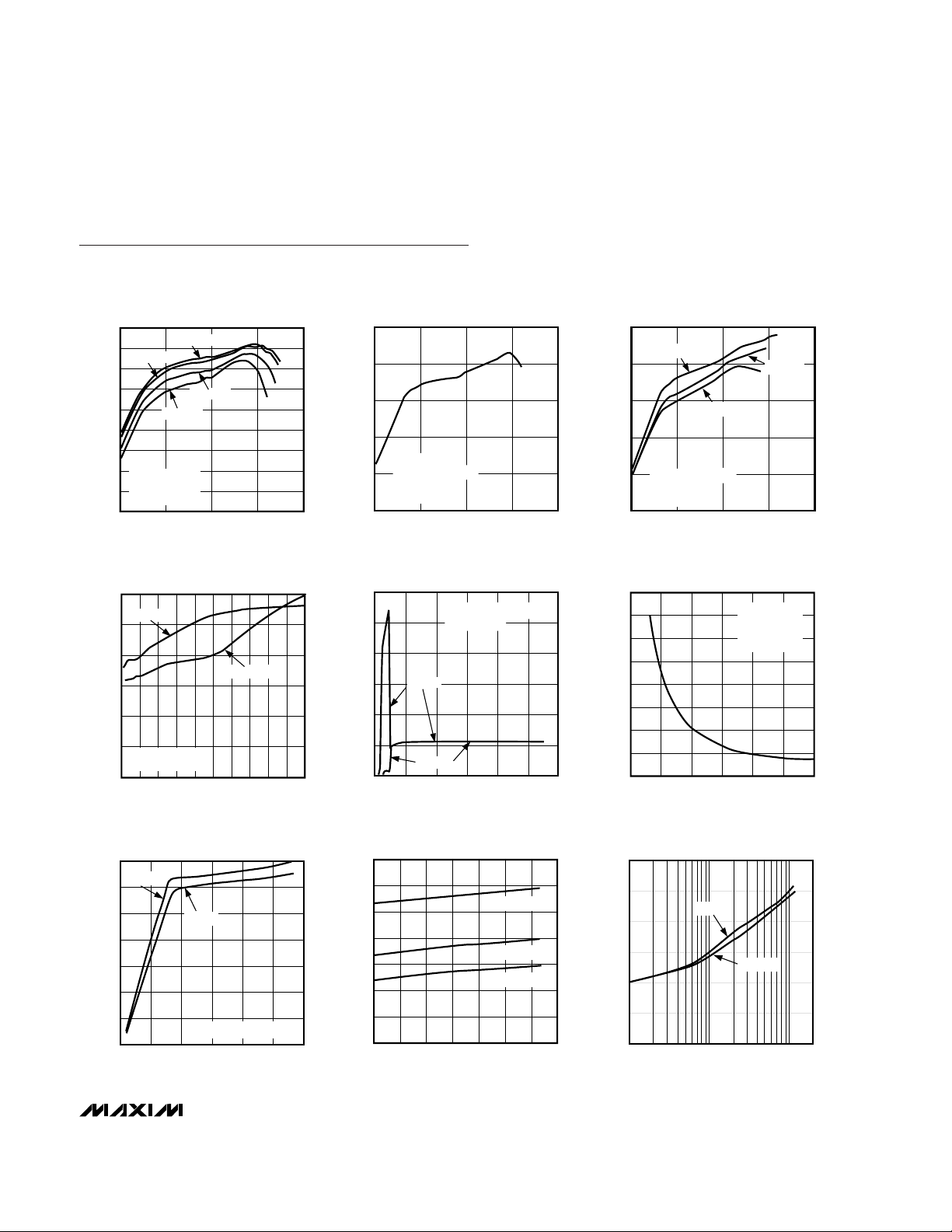
EFFICIENCY vs. LOAD CURRENT
(V
OUT
= 5V)
MAX668 toc01
LOAD CURRENT (mA)
EFFICIENCY (%)
55
VIN = 3.3V
VIN = 3.6V
VIN = 2V
VIN = 2.7V
BOOTSTRAPPED
FIGURE 3
R4 = 200kΩ
70
1 10,000100010 100
MAX668 EFFICIENCY vs.
LOAD CURRENT (V
OUT
= 12V)
85
75
95
80
90
MAX668 toc02
LOAD CURRENT (mA)
EFFICIENCY (%)
VIN = 5V
NON-BOOTSTRAPPED
FIGURE 4
R4 = 200kΩ
MAX668 EFFICIENCY vs.
LOAD CURRENT (V
OUT
= 24V)
MAX668 toc03
LOAD CURRENT (mA)
EFFICIENCY (%)
70
1 10,000100010 100
85
75
95
80
90
VIN = 8V
VIN = 5V
VIN = 12V
NON-BOOTSTRAPPED
FIGURE 4
R4 = 200kΩ
0
1.5
1.0
0.5
2.0
2.5
3.0
0 400300100 200 500 600 700 800 900 1000
MAX669 MINIMUM START-UP VOLTAGE
vs. LOAD CURRENT
MAX668 toc04
LOAD CURRENT (mA)
MINIMUM START-UP VOLTAGE (V)
V
OUT
= 5V
V
OUT
= 12V
BOOTSTRAPPED
FIGURE 2
0
0.5
1.5
2.0
2.5
3.0
3.5
0105 15202530
SHUTDOWN CURRENT vs.
SUPPLY VOLTAGE
MAX668 toc07
SUPPLY VOLTAGE (V)
SHUTDOWN CURRENT (µA)
1.0
CURRENT INTO VCC PIN
MAX668
MAX669
0
400
200
800
600
1000
1200
010155 202530
SUPPLY CURRENT vs.
SUPPLY VOLTAGE
MAX668 toc05
SUPPLY VOLTAGE (V)
SUPPLY CURRENT (µA)
MAX669
MAX668
CURRENT INTO VCC PIN
R
OSC
= 500kΩ
0
500
1000
2000
2500
3000
3500
4000
042681012
NO-LOAD SUPPLY CURRENT vs.
SUPPLY VOLTAGE
MAX668 toc06
SUPPLY VOLTAGE (V)
NO-LOAD SUPPLY CURRENT (µA)
1500
V
OUT
= 12V
BOOTSTRAPPED
FIGURE 2
R4 = 200kΩ
150
190
210
170
250
230
270
290
-40 -20 0 20 40 60 80 100
SUPPLY CURRENT vs.
TEMPERATURE
MAX668 toc08
TEMPERATURE (°C)
SUPPLY CURRENT (µA)
R
OSC
= 100kΩ
R
OSC
= 200kΩ
R
OSC
= 500kΩ
0.1 1 10 20
LDO DROPOUT VOLTAGE vs.
LDO CURRENT
MAX668 toc09
LDO CURRENT (mA)
LDO DROPOUT VOLTAGE (mV)
300
0
50
100
150
200
250
VIN = 3V
VIN = 4.5V
Typical Operating Characteristics
(Circuits of Figures 2, 3, 4, and 5; TA= +25°C; unless otherwise noted.)
Page 6
MAX668/MAX669
1.8V to 28V Input, PWM Step-Up
Controllers in µMAX
6 _______________________________________________________________________________________
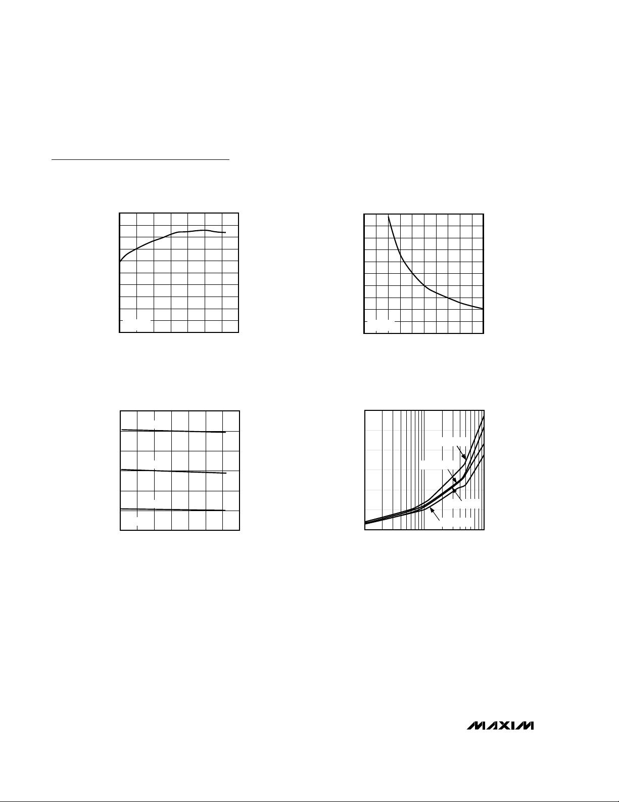
Typical Operating Characteristics (continued)
(Circuits of Figures 2, 3, 4, and 5; TA= +25°C; unless otherwise noted.)
1.240
1.242
1.243
1.241
1.245
1.246
1.244
1.248
1.249
1.247
1.250
-40 -20 0 20 40 60 80 100
REFERENCE VOLTAGE vs.
TEMPERATURE
MAX668 toc10
TEMPERATURE (°C)
REFERENCE VOLTAGE (V)
VCC = 5V
0
100
150
50
250
300
200
400
450
350
500
0 100 200 300 400 500
SWITCHING FREQUENCY vs. R
OSC
MAX668 toc11
R
OSC
(kΩ)
SWITCHING FREQUENCY (kHz)
VCC = 5V
0
100
300
400
500
600
-40 0-20 20 40 60 80 100
SWITCHING FREQUENCY vs.
TEMPERATURE
MAX668 toc12
TEMPERATURE (°C)
SWITCHING FREQUENCY (kHz)
200
100kΩ
165kΩ
499kΩ
VIN = 5V
100 1000 10,000
EXT RISE/FALL TIME vs.
CAPACITANCE
MAX668 toc13
CAPACITANCE (pF)
EXT RISE/FALL TIME (ns)
60
0
10
20
30
40
50
tR, VCC = 3.3V
tF, VCC = 3.3V
tR, VCC = 5V
tF, VCC = 5V
Page 7

MAX668/MAX669
1.8V to 28V Input, PWM Step-Up
Controllers in µMAX
_______________________________________________________________________________________
7
EXITING SHUTDOWN
MAX668 toc14
OUTPUT
VOLTAGE
5V/div
INDUCTOR
CURRENT
2A/div
SHUTDOWN
VOLTAGE
5V/div
MAX668, V
IN
= 5V, V
OUT
= 12V, LOAD = 1.0A, R
OSC
= 100kΩ,
LOW VOLTAGE, NON-BOOTSTRAPPED
500µs/div
0V
0V
0A
ENTERING SHUTDOWN
MAX668 toc15
OUTPUT
VOLTAGE
5V/div
SHUTDOWN
VOLTAGE
5V/div
MAX668, V
IN
= 5V, V
OUT
= 12V, LOAD = 1.0A,
LOW VOLTAGE, NON-BOOTSTRAPPED
200µs/div
0V
0V
HEAVY-LOAD SWITCHING WAVEFORM
MAX668 toc16
V
OUT
200mV/div
AC-COUPLED
I
L
1A/div
Q1, DRAIN
5V/div
MAX668, V
IN
= 5V, V
OUT
= 12V, I
LOAD
= 1.0A,
LOW VOLTAGE, NON-BOOTSTRAPPED
1µs/div
0V
0A
LOAD-TRANSIENT RESPONSE
MAX668 toc18
OUTPUT
VOLTAGE
AC-COUPLED
100mV/div
LOAD
CURRENT
1A/div
MAX668, V
IN
= 5V, V
OUT
= 12V, I
LOAD
= 0.1A TO 1.0A,
LOW VOLTAGE, NON-BOOTSTRAPPED
1ms/div
LIGHT-LOAD SWITCHING WAVEFORM
MAX668 toc17
V
OUT
100mV/div
AC-COUPLED
I
L
1A/div
Q1, DRAIN
5V/div
MAX668, V
IN
= 5V, V
OUT
= 12V, I
LOAD
= 0.1A,
LOW VOLTAGE, NON-BOOTSTRAPPED
1µs/div
0V
0A
Typical Operating Characteristics (continued)
(Circuits of Figures 2, 3, 4, and 5; TA= +25°C; unless otherwise noted.)
LINE-TRANSIENT RESPONSE
MAX668 toc19
INPUT
VOLTAGE
5V/div
0V
OUTPUT
VOLTAGE
100mV/div
AC-COUPLED
MAX668, V
IN
= 5V TO 8V, V
OUT
= 12V, LOAD = 1.0A,
HIGH VOLTAGE, NON-BOOTSTRAPPED
20ms/div
Page 8

Detailed Description
The MAX668/MAX669 current-mode PWM controllers
operate in a wide range of DC-DC conversion applications, including boost, SEPIC, flyback, and isolated output configurations. Optimum conversion efficiency is
maintained over a wide range of loads by employing
both PWM operation and Maxim’s proprietary Idle
Mode control to minimize operating current at light
loads. Other features include shutdown, adjustable
internal operating frequency or synchronization to an
external clock, soft start, adjustable current limit, and a
wide (1.8V to 28V) input range.
MAX668 vs. MAX669 Differences
Differences between the MAX668 and MAX669 relate
to their use in bootstrapped or non-bootstrapped circuits (Table 1). The MAX668 operates with inputs as
low as 3V and can be connected in
either
a bootstrapped or non-bootstrapped (IC powered from input
supply or other source) configuration. When not bootstrapped, the MAX668 has no restriction on output voltage. When bootstrapped, the output cannot exceed
28V.
The MAX669 is optimized for low input voltages (down
to 1.8V) and
requires
bootstrapped operation (IC pow-
ered from V
OUT
) with output voltages no greater than
28V. Bootstrapping is required because the MAX669
does not have undervoltage lockout, but instead drives
EXT with an open-loop, 50% duty-cycle start-up oscillator when LDO is below 2.5V. It switches to closed-loop
operation only when LDO exceeds 2.5V. If a non-bootstrapped connection is used with the MAX669 and if
VCC(the input voltage) remains below 2.7V, the output
voltage will soar above the regulation point. Table 2
recommends the appropriate device for each biasing
option.
MAX668/MAX669
1.8V to 28V Input, PWM Step-Up
Controllers in µMAX
8 _______________________________________________________________________________________
NAME FUNCTION
1 LDO
5V On-Chip Regulator Output. This regulator powers all internal circuitry including the EXT gate driver.
Bypass LDO to GND with a 1µF or greater ceramic capacitor.
2 FREQ
Oscillator Frequency Set Input. A resistor from FREQ to GND sets the oscillator from 100kHz (R
OSC
=
500kΩ) to 500kHz (R
OSC
= 100kΩ). f
OSC
= 5 x 10
10
/ R
OSC
. R
OSC
is still required if an external clock is used
at SYNC/SHDN. (See
SYNC/SHDN and FREQ Inputs
section.)
PIN
3 GND Analog Ground
7 PGND Power Ground for EXT Gate Driver and Negative Current-Sense Input
6 CS+ Positive Current-Sense Input. Connect a current-sense resistor, RCS, between CS+ and PGND.
5 FB Feedback Input. The FB threshold is 1.25V.
4 REF 1.25V Reference Output. REF can source 50µA. Bypass to GND with a 0.22µF ceramic capacitor.
10
SYNC/
SHDN
Shutdown control and Synchronization Input. There are three operating modes:
• SYNC/SHDN low: DC-DC off.
• SYNC/SHDN high: DC-DC on with oscillator frequency set at FREQ by R
OSC
.
• SYNC/SHDN clocked: DC-DC on with operating frequency set by SYNC clock input. DC-DC conversion
cycles initiate on rising edge of input clock.
9 V
CC
Input Supply to On-Chip LDO Regulator. VCCaccepts inputs up to 28V. Bypass to GND with a 0.1µF ceramic
capacitor.
8 EXT External MOSFET Gate-Driver Output. EXT swings from LDO to PGND.
Pin Description
Table 1. MAX668/MAX669 Comparison
MAX668 MAX669
VCCInput
Range
3V to 28V 1.8V to 28V
Operation
Bootstrapped or nonbootstrapped. VCCcan be connected to input, output, or
other voltage source such as
a logic supply.
Must be bootstrapped (V
CC
must be connected to boosted output voltage, V
OUT
).
Undervoltage
Lockout
IC stops switching for LDO
below 2.5V.
No
Soft-Start Yes
When LDO is
above 2.5V
FEATURE
Page 9

PWM Controller
The heart of the MAX668/MAX669 current-mode PWM
controller is a BiCMOS multi-input comparator that
simultaneously processes the output-error signal, the
current-sense signal, and a slope-compensation ramp
(Figure 1). The main PWM comparator is direct summing, lacking a traditional error amplifier and its associated phase shift. The direct summing configuration
approaches ideal cycle-by-cycle control over the output voltage since there is no conventional error amp in
the feedback path.
In PWM mode, the controller uses fixed-frequency, current-mode operation where the duty ratio is set by the
input/output voltage ratio (duty ratio = (V
OUT
- VIN) / V
IN
in the boost configuration). The current-mode feedback
loop regulates peak inductor current as a function of
the output error signal.
At light loads the controller enters Idle Mode. During
Idle Mode, switching pulses are provided only as needed to service the load, and operating current is minimized to provide best light-load efficiency. The
minimum-current comparator threshold is 15mV, or 15%
of the full-load value (I
MAX
) of 100mV. When the controller is synchronized to an external clock, Idle Mode
occurs only at very light loads.
Bootstrapped/Non-Bootstrapped Operation
Low-Dropout Regulator (LDO)
Several IC biasing options, including bootstrapped and
non-bootstrapped operation, are made possible by an
on-chip, low-dropout 5V regulator. The regulator input is
at VCC, while its output is at LDO. All MAX668/MAX669
functions, including EXT, are internally powered from
LDO. The VCC-to-LDO dropout voltage is typically
200mV (300mV max at 12mA), so that when VCCis less
than 5.2V, LDO is typically V
CC
- 200mV. When LDO is
in dropout, the MAX668/MAX669 still operate with V
CC
as low as 3V (as long as LDO exceeds 2.7V), but with
reduced amplitude FET drive at EXT. The maximum
VCCinput voltage is 28V.
LDO can supply up to 12mA to power the IC, supply
gate charge through EXT to the external FET, and supply small external loads. When driving particularly large
FETs at high switching rates, little or no LDO current
may be available for external loads. For example, when
switched at 500kHz, a large FET with 20nC gate charge
requires 20nC x 500kHz, or 10mA.
VCCand LDO allow a variety of biasing connections to
optimize efficiency, circuit quiescent current, and fullload start-up behavior for different input and output
voltage ranges. Connections are shown in Figures 2, 3,
4, and 5. The characteristics of each are outlined in
Table 1.
MAX668/MAX669
1.8V to 28V Input, PWM Step-Up
Controllers in µMAX
_______________________________________________________________________________________ 9
ANTISAT
MUX
LOW-VOLTAGE
START-UP
OSCILLATOR
(MAX669 ONLY)
+A
-A
X6
+C
-C
X1
+S
-S
X1
SLOPE COMPENSATION
SQ
BIAS
OSC OSC
FREQ
SYNC/SHDN
0
1
LDO
PGND
1.25V
REF
EXT
UVLO
V
CC
R1
552k
R2
276k
R3
276k
100mV
15mV
I
MAX
I
MIN
MAIN PWM
COMPARATOR
1.25V
FB
CURRENT SENSE
CS+
MAX668
MAX669
LDO
MAX669 ONLY
R
Figure 1. MAX668/MAX669 Functional Diagram
Page 10

MAX668/MAX669
1.8V to 28V Input, PWM Step-Up
Controllers in µMAX
10 ______________________________________________________________________________________
MAX669
LDO
CS+
REF
FREQ
V
CC
SYNC/
SHDN
PGND
FB
GND
N1
EXT
VIN = 1.8V to 12V
C3
0.22µF
C2
0.1µF
C4
1µF
R4
100k
1%
R1
0.02Ω
R2
218k
1%
R3
24.9k
1%
C7
220pF
D1
MBRS340T3
C5
68µF
20V
C6
68µF
20V
C8
0.1µF
3
5
7
6
8
2
4
9
1
10
V
OUT
= 12V @ 0.5A
C1
68µF
20V
L1
4.7µH
IRF7401
Figure 2. MAX669 High-Voltage Bootstrapped Configuration
MAX669
LDO
CS+
REF
FREQ
V
CC
SYNC/
SHDN
PGND
FB
GND
N1
EXT
VIN = 1.8V to 5V
C3
0.22µF
C2
1µF
R4
100k
1%
R1
0.02Ω
R2
75k
1%
R3
24.9k
1%
C7
220pF
D1
MBRS340T3
C4
68µF
10V
C5
68µF
10V
C6
0.1µF
3
5
7
6
8
2
4
9
1
10
V
OUT
= 5V @ 1A
C1
68µF
10V
L1
4.7µH
FDS6680
IRF7401
Figure 3. MAX669 Low-Voltage Bootstrapped Configuration
Bootstrapped Operation
With bootstrapped operation, the IC is powered from
the circuit output (V
OUT
). This improves efficiency
when the input voltage is low, since EXT drives the FET
with a higher gate voltage than would be available from
the low-voltage input. Higher gate voltage reduces the
FET on-resistance, increasing efficiency. Other (undesirable) characteristics of bootstrapped operation are
increased IC operating power (since it has a higher
operating voltage) and reduced ability to start up with
high load current at low input voltages. If the input volt-
age range extends below 2.7V, then bootstrapped
operation with the MAX669 is the only option.
With VCCconnected to V
OUT
, as in Figure 2, EXT volt-
age swing is 5V when VCCis 5.2V or more, and V
CC
-
0.2V when VCCis less than 5.2V. If the output voltage
does not exceed 5.5V, the on-chip regulator can be
disabled by connecting VCCto LDO (Figure 3). This
eliminates the LDO forward drop and supplies maximum gate drive to the external FET.
Page 11

Non-Bootstrapped Operation
With non-bootstrapped operation, the IC is powered
from the input voltage (VIN) or another source, such as
a logic supply. Non-bootstrapped operation (Figure 4)
is recommended (but not required) for input voltages
above 5V, since the EXT amplitude (limited to 5V by
LDO) at this voltage range is no higher than it would be
with bootstrapped operation. Note that non-bootstrapped operation is
required
if the output voltage
exceeds 28V, since this level is too high to safely con-
nect to VCC. Also note that only the MAX668 can be
used with non-bootstrapped operation.
If the input voltage does not exceed 5.5V, the on-chip
regulator can be disabled by connecting VCCto LDO
(Figure 5). This eliminates the regulator forward drop
and supplies the maximum gate drive to the external
FET for lowest on-resistance. Disabling the regulator
also reduces the non-bootstrapped minimum input voltage from 3V to 2.7V.
MAX668/MAX669
1.8V to 28V Input, PWM Step-Up
Controllers in µMAX
______________________________________________________________________________________ 11
MAX668
LDO
CS+
REF
FREQ
V
CC
SYNC
/
SHDN
PGND
FB
GND
N1
EXT
VIN = 2.7V to 5.5V
C3
0.22µF
C2
1µF
R4
100k
1%
R1
0.02Ω
R2
218k
1%
R3
24.9k
1%
C7
220pF
D1
MBRS340T3
C4
68µF
20V
C5
68µF
20V
C6
0.1µF
3
5
7
6
8
2
4
9
1
10
V
OUT
= 12V @ 1A
C1
68µF
10V
L1
4.7µH
FDS6680
Figure 5. MAX668 Low-Voltage Non-Bootstrapped Configuration
MAX668
LDO
CS+
REF
FREQ
V
CC
PGND
FB
GND
N1
EXT
VIN = 3V to 12V
C3
0.22µF
C4
1µF
C2
0.1µF
R4
100k
1%
R1
0.02Ω
R2
218k
1%
R3
24.9k
1%
C7
220pF
D1
MBRS340T3
C5
68µF
20V
C6
68µF
20V
C8
0.1µF
3
5
7
6
8
2
4
9
1
10
V
OUT
= 12V @ 1A
C1
68µF
20V
L1
4.7µH
FDS6680
SYNC/
SHDN
Figure 4. MAX668 High-Voltage Non-Bootstrapped Configuration
Page 12

MAX668/MAX669
1.8V to 28V Input, PWM Step-Up
Controllers in µMAX
12 ______________________________________________________________________________________
Table 2. Bootstrapped and Non-Bootstrapped Configurations
CONFIGURATION FIGURE
USE
WITH:
INPUT
VOLTAGE
RANGE* (V)
OUTPUT
VOLTAGE
RANGE (V)
COMMENTS
High-Voltage,
Bootstrapped
Figure
2
MAX669 1.8 to 28 3V to 28
Connect VCCto V
OUT
. Provides maximum external
FET gate drive for low-voltage (Input <3V) to highvoltage (output >5.5V) boost circuits. V
OUT
cannot
exceed 28V.
Low-Voltage,
Bootstrapped
Figure
3
MAX669 1.8 to 5.5 2.7 to 5.5
Connect V
OUT
to VCCand LDO. Provides maxi-
mum possible external FET gate drive for low-voltage designs, but limits V
OUT
to 5.5V or less.
High-Voltage,
Non-Bootstrapped
Figure
4
MAX668 3 to 28 VINto ∞
Connect VINto VCC. Provides widest input and out-
put range, but external FET gate drive is reduced for
V
IN
below 5V.
Low-Voltage,
Non-Bootstrapped
Figure
5
MAX668 2.7 to 5.5 VINto ∞
Connect VINto VCCand LDO. FET gate-drive
amplitude = V
IN
for logic-supply (input 3V to 5.5V) to
high-voltage (output >5.5V) boost circuits. IC operating power is less than in Figure 4, since IC current
does not pass through the LDO regulator.
Extra IC supply,
Non-Bootstrapped
None MAX668
Not
Restricted
VINto ∞
Connect VCC and LDO to a separate supply
(V
BIAS
) that powers only the IC. FET gate-drive
amplitude = V
BIAS
. Input power source (V
IN)
and
output voltage range (V
OUT
) are not restricted,
except that V
OUT
must exceed VIN.
In addition to the configurations shown in Table 2, the
following guidelines may help when selecting a configuration:
1) If VINis ever below 2.7V, V
CC
must
be boot-
strapped to V
OUT
and the MAX669 must be used. If
V
OUT
never exceeds 5.5V, LDO may be shorted to
VCCand V
OUT
to eliminate the dropout voltage of
the LDO regulator.
2) If VINis greater than 3.0V, VCCcan be powered
from VIN, rather than from V
OUT
(non-bootstrapped).
This can save quiescent power consumption, especially when V
OUT
is large. If VINnever exceeds
5.5V, LDO may be shorted to VCCand VINto eliminate the dropout voltage of the LDO regulator.
3) If VINis in the 3V to 4.5V range (i.e., 1-cell Li-Ion or
3-cell NiMH battery range), bootstrapping VCCfrom
V
OUT
, although not required, may increase overall
efficiency by increasing gate drive (and reducing
FET resistance) at the expense of quiescent power
consumption.
4) If VINalways exceeds 4.5V, VCCshould be tied to
VIN, since bootstrapping from V
OUT
does not
increase gate drive from EXT but does increase
quiescent power dissipation.
*
For standard step-up DC-DC circuits (as in Figures 2, 3, 4, and 5), regulation cannot be maintained if VINexceeds V
OUT
. SEPIC
and transformer-based circuits do not have this limitation.
Page 13

SYNC/
SHDN
and FREQ Inputs
The SYNC/SHDN pin provides both external-clock synchronization (if desired) and shutdown control. When
SYNC/SHDN is low, all IC functions are shut down. A
logic high at SYNC/SHDN selects operation at a frequency set by R
OSC
, connected from FREQ to GND.
The relationship between f
OSC
and R
OSC
is:
R
OSC
= 5 x 10
10
/ f
OSC
So a 500kHz operating frequency, for example, is set
with R
OSC
= 100kΩ.
Rising clock edges on SYNC/SHDN are interpreted as
synchronization inputs. If the sync signal is lost while
SYNC/SHDN is high, the internal oscillator takes over at
the end of the last cycle and the frequency is returned
to the rate set by R
OSC
. If sync is lost with SYNC/SHDN
low, the IC waits for 70µs before shutting down. This
maintains output regulation even with intermittent sync
signals. When an external sync signal is used, Idle
Mode switchover at the 15mV current-sense threshold
is disabled so that Idle Mode only occurs at very light
loads. Also, R
OSC
should be set for a frequency 15%
below the SYNC clock rate:
R
OSC(SYNC)
= 5 x 10
10
/ (0.85 x f
SYNC
)
Soft-Start
The MAX668/MAX669 feature a “digital” soft start which
is preset and requires no external capacitor. Upon
start-up, the peak inductor increments from 1/5 of the
value set by RCS, to the full current-limit value, in five
steps over 1024 cycles of f
OSC
or f
SYNC
. For example,
with an f
OSC
of 200kHz, the complete soft-start
sequence takes 5ms. See the
Typical Operating
Characteristics
for a photo of soft-start operation. Softstart is implemented: 1) when power is first applied to
the IC, 2) when exiting shutdown with power already
applied, and 3) when exiting undervoltage lockout. The
MAX669’s soft-start sequence does not start until LDO
reaches 2.5V.
Design Procedure
The MAX668/MAX669 can operate in a number of DCDC converter configurations including step-up, SEPIC
(single-ended primary inductance converter), and flyback. The following design discussions are limited to
step-up, although SEPIC and flyback examples are
shown in the
Application Circuits
section.
Setting the Operating Frequency
The MAX668/MAX669 can be set to operate from
100kHz to 500kHz. Choice of operating frequency will
depend on number of factors:
1) Noise considerations may dictate setting (or synchronizing) f
OSC
above or below a certain frequency
or band of frequencies, particularly in RF applications.
2) Higher frequencies allow the use of smaller value
(hence smaller size) inductors and capacitors.
3) Higher frequencies consume more operating power
both to operate the IC and to charge and discharge
the gate of the external FET. This tends to reduce
efficiency at light loads; however, the MAX668/
MAX669’s Idle Mode feature substantially increases
light-load efficiency.
4) Higher frequencies may exhibit poorer overall efficiency due to more transition losses in the FET;
however, this shortcoming can often be nullified by
trading some of the inductor and capacitor size
benefits for lower-resistance components.
The oscillator frequency is set by a resistor, R
OSC
, con-
nected from FREQ to GND. R
OSC
must be connected
whether or not the part is externally synchronized R
OSC
is in each case:
R
OSC
= 5 x 10¹⁰/ f
OSC
when
not
using an external clock.
R
OSC(SYNC)
= 5 x 10
10
/ (0.85 x f
SYNC
)
when using an external clock, f
SYNC
.
Setting the Output Voltage
The output voltage is set by two external resistors (R2
and R3, Figures 2, 3, 4, and 5). First select a value for
R3 in the 10kΩ to 1MΩ range. R2 is then given by:
R2 = R3 [(V
OUT
/ V
REF
) – 1]
where V
REF
is 1.25V.
Determining Inductance Value
For most MAX668/MAX669 boost designs, the inductor
value (L
IDEAL
) can be derived from the following equation, which picks the optimum value for stability based
on the MAX668/MAX669’s internally set slope compensation:
L
IDEAL
= V
OUT
/ (4 x I
OUT
x f
OSC
)
The MAX668/MAX669 allow significant latitude in inductor selection if L
IDEAL
is not a convenient value. This
may happen if L
IDEAL
is a not a standard inductance
(such as 10µH, 22µH, etc.), or if L
IDEAL
is too large to
be obtained with suitable resistance and saturation-current rating in the desired size. Inductance values smaller than L
IDEAL
may be used with no adverse stability
effects; however, the peak-to-peak inductor current
(I
LPP
) will rise as L is reduced. This has the effect of
raising the required I
LPK
for a given output power and
also requiring larger output capacitance to maintain a
MAX668/MAX669
1.8V to 28V Input, PWM Step-Up
Controllers in µMAX
______________________________________________________________________________________ 13
Page 14

MAX668/MAX669
given output ripple. An inductance value larger than
L
IDEAL
may also be used, but output-filter capacitance
must be increased by the same proportion that L has to
L
IDEAL
. See the
Capacitor Selection
section for more
information on determining output filter values.
Due the MAX668/MAX669’s high switching frequencies,
inductors with a ferrite core or equivalent are recommended. Powdered iron cores are
not
recommended
due to their high losses at frequencies over 50kHz.
Determining Peak Inductor Current
The peak inductor current required for a particular output is:
I
LPEAK
= I
LDC
+ (I
LPP
/ 2)
where I
LDC
is the average DC input current and I
LPP
is
the inductor peak-to-peak ripple current. The I
LDC
and
I
LPP
terms are determined as follows:
where VDis the forward voltage drop across the
Schottky rectifier diode (D1), and VSWis the drop
across the external FET, when on.
where L is the inductor value. The saturation rating of
the selected inductor should meet or exceed the calculated value for I
LPEAK
, although most coil types can be
operated up to 20% over their saturation rating without
difficulty. In addition to the saturation criteria, the inductor should have as low a series resistance as possible.
For continuous inductor current, the power loss in the
inductor resistance, PLR, is approximated by:
P
LR
≅ (I
OUT
x V
OUT
/ VIN)2x R
L
where RLis the inductor series resistance.
Once the peak inductor current is selected, the current-
sense resistor (RCS) is determined by:
RCS= 85mV / I
LPEAK
For high peak inductor currents (>1A), Kelvin sensing
connections should be used to connect CS+ and
PGND to RCS. PGND and GND should be tied together
at the ground side of RCS.
Power MOSFET Selection
The MAX668/MAX669 drive a wide variety of N-channel
power MOSFETs (NFETs). Since LDO limits the EXT
output gate drive to no more than 5V, a logic-level
NFET is required. Best performance, especially at low
input voltages (below 5V), is achieved with low-thresh-
old NFETs that specify on-resistance with a gatesource voltage (VGS) of 2.7V or less. When selecting an
NFET, key parameters can include:
1) Total gate charge (Qg)
2) Reverse transfer capacitance or charge (C
RSS
)
3) On-resistance (R
DS(ON)
)
4) Maximum drain-to-source voltage (V
DS(MAX)
)
5) Minimum threshold voltage (V
TH(MIN)
)
At high switching rates, dynamic characteristics (parameters 1 and 2 above) that predict switching losses
may have more impact on efficiency than R
DS(ON),
which predicts DC losses. Qgincludes all capacitances
associated with charging the gate. In addition, this
parameter helps predict the current needed to drive the
gate at the selected operating frequency. The continuous LDO current for the FET gate is:
I
GATE
= Qgx f
OSC
For example, the MMFT3055L has a typical Qgof 7nC
(at V
GS
= 5V); therefore, the I
GATE
current at 500kHz is
3.5mA. Use the FET manufacturer’s
typical
value for Q
g
in the above equation, since a maximum value (if supplied) is usually too conservative to be of use in estimating I
GATE
.
Diode Selection
The MAX668/MAX669’s high switching frequency
demands a high-speed rectifier. Schottky diodes are
recommended for most applications because of their
fast recovery time and low forward voltage. Ensure that
the diode’s average current rating is adequate using
the diode manufacturer’s data, or approximate it with
the following formula:
Also, the diode reverse breakdown voltage must
exceed V
OUT
. For high output voltages (50V or above),
Schottky diodes may not be practical because of this
voltage requirement. In these cases, use a high-speed
silicon rectifier with adequate reverse voltage.
Capacitor Selection
Output Filter Capacitor
The minimum output filter capacitance that ensures stability is:
where V
IN(MIN)
is the minimum expected input voltage.
Typically C
OUT(MIN)
, though sufficient for stability, will
C
(7.5V x L / L )
(2 R x V x f )
OUT(MIN)
IDEAL
CS IN(MIN) OSC
=
π
II
I- I
3
DIODE OUT
LPEAK OUT
=+
1.8V to 28V Input, PWM Step-Up
Controllers in µMAX
14 ______________________________________________________________________________________
I =
I (V + V
(V – V
LDC
OUT OUT D
IN SW
)
)
I =
(V – V ) (V + V – V )
L x f (V + V )
LPP
IN SW OUT D IN
OSC OUT D
Page 15

not be adequate for low output voltage ripple. Since
output ripple in boost DC-DC designs is dominated by
capacitor equivalent series resistance (ESR), a capacitance value 2 or 3 times larger than C
OUT(MIN)
is typically needed. Low-ESR types must be used. Output
ripple due to ESR is:
V
RIPPLE(ESR)
= I
LPEAK
x ESR
COUT
Input Capacitor
The input capacitor (CIN) in boost designs reduces the
current peaks drawn from the input supply and reduces
noise injection. The value of CINis largely determined
by the source impedance of the input supply. High
source impedance requires high input capacitance,
particularly as the input voltage falls. Since step-up DCDC converters act as “constant-power” loads to their
input supply, input current rises as input voltage falls.
Consequently, in low-input-voltage designs, increasing
CINand/or lowering its ESR can add as many as five
percentage points to conversion efficiency. A good
starting point is to use the same capacitance value for
CINas for C
OUT
.
Bypass Capacitors
In addition to CINand C
OUT
, three ceramic bypass
capacitors are also required with the MAX668/MAX669.
Bypass REF to GND with 0.22µF or more. Bypass LDO
to GND with 1µF or more. And bypass VCCto GND with
0.1µF or more. All bypass capacitors should be located
as close to their respective pins as possible.
Compensation Capacitor
Output ripple voltage due to C
OUT
ESR affects loop
stability by introducing a left half-plane zero. A small
capacitor connected from FB to GND forms a pole with
the feedback resistance that cancels the ESR zero. The
optimum compensation value is:
where R2 and R3 are the feedback resistors (Figures 2,
3, 4, and 5). If the calculated value for CFBresults in a
non-standard capacitance value, values from 0.5C
FB
to
1.5C
FB
will also provide sufficient compensation.
Applications Information
Starting Under Load
In non-bootstrapped configurations (Figures 4 and 5),
the MAX668 can start up with any combination of output load and input voltage at which it can operate when
already started. In other words, there are no special
limitations to start-up in non-bootstrapped circuits.
In bootstrapped configurations with the MAX668 or
MAX669, there may be circumstances where full load
current can only be applied after the circuit has started
and the output is near its set value. As the input voltage
drops, this limitation becomes more severe. This characteristic of all bootstrapped designs occurs when the
MOSFET gate is not fully driven until the output voltage
rises. This is problematic because a heavily loaded output cannot rise until the MOSFET has low on-resistance. In such situations, low-threshold FETs (V
TH
<
V
IN(MIN)
) are the most effective solution. The
Typical
Operating Characteristics
section shows plots of startup voltage versus load current for a typical bootstrapped design.
Layout Considerations
Due to high current levels and fast switching waveforms
that radiate noise, proper PC board layout is essential.
Protect sensitive analog grounds by using a star ground
configuration. Minimize ground noise by connecting
GND, PGND, the input bypass-capacitor ground lead,
and the output-filter ground lead to a single point (star
ground configuration). Also, minimize trace lengths to
reduce stray capacitance, trace resistance, and radiated noise. The trace between the external gain-setting
resistors and the FB pin must be extremely short, as
must the trace between GND and PGND.
Application Circuits
Low-Voltage Boost Circuit
Figure 3 shows the MAX669 operating in a low-voltage
boost application. The MAX669 is configured in the
bootstrapped mode to improve low input voltage performance. The IRF7401 N-channel MOSFET was selected for Q1 in this application because of its very low
0.7V gate threshold voltage (VGS). This circuit provides
a 5V output at greater than 2A of output current and
operates with input voltages as low as 1.8V. Efficiency
is typically in the 85% to 90% range.
+12V Boost Application
Figure 5 shows the MAX668 operating in a 5V to 12V
boost application. This circuit provides output currents
of greater than 1A at a typical efficiency of 92%. The
MAX668 is operated in non-bootstrapped mode to minimize the input supply current. This achieves maximum
light-load efficiency. If input voltages below 5V are
used, the IC should be operated in bootstrapped mode
to achieve best low-voltage performance.
4-Cell to +5V SEPIC Power Supply
Figure 6 shows the MAX668 in a SEPIC (single-ended
primary inductance converter) configuration. This configuration is useful when the input voltage can be either
MAX668/MAX669
1.8V to 28V Input, PWM Step-Up
Controllers in µMAX
______________________________________________________________________________________ 15
C C x
ESR
(R2 x R3) / (R2 + R3)
FB OUT
COUT
=
Page 16

MAX668/MAX669
larger or smaller than the output voltage, such as when
converting four NiMH, NiCd, or Alkaline cells to a 5V
output. The SEPIC configuration is often a good choice
for combined step-up/step-down applications.
The N-channel MOSFET (Q1) must be selected to withstand a drain-to-source voltage (VDS) greater than the
sum of the input and output voltages. The coupling
capacitor (C2) must be a low-ESR type to achieve maximum efficiency. C2 must also be able to handle high
ripple currents; ordinary tantalum capacitors should not
be used for high-current designs.
The circuit in Figure 6 provides greater than 1A output
current at 5V when operating with an input voltage from
3V to 25V. Efficiency will typically be between 70% and
85%, depending upon the input voltage and output current.
Isolated +5V to +5V Power Supply
The circuit of Figure 7 provides a 5V isolated output at
400mA from a 5V input power supply. Transformer T1
provides electrical isolation for the forward path of the
converter, while the TLV431 shunt regulator and
MOC211 opto-isolator provide an isolated feedback
error voltage for the converter. The output voltage is set
by resistors R2 and R3 such that the mid-point of the
divider is 1.24V (threshold of TLV431). Output voltage
can be adjusted from 1.24V to 6V by selecting the
proper ratio for R2 and R3. For output voltages greater
than 6V, substitute the TL431 for the TLV431, and use
2.5V as the voltage at the midpoint of the voltagedivider.
1.8V to 28V Input, PWM Step-Up
Controllers in µMAX
16 ______________________________________________________________________________________
R3
100k
R4
0.02Ω
R1
75k
R2
25k
C4
520pF
V
IN
3V to 25V
30V
FDS6680
Q1
L1
CTX5-4
MAX668
SHDNV
CC
910
LDO
FREQ
D1: MBR5340T3, 3A, 40V SCHOTTKY DIODE
R4: WSL-2512-R020F, 0.02Ω
C3: AVX TPSZ686M020R0150, 68µF, 150mΩ ESR
REF
EXT
CS+
8
6
PGNDGND
73
FB
1
2
4
5
1µF
22µF x 3
@ 35V
C3
68µF x 3
V
OUT
5V @ 1A
4.9µH
C2
10µF @ 35V
D1
40V
0.22µF
Figure 6. MAX668 in SEPIC Configuration
Page 17

Chip Information
TRANSISTOR COUNT: 1861
MAX668/MAX669
1.8V to 28V Input, PWM Step-Up
Controllers in µMAX
______________________________________________________________________________________ 17
MAX668
LDO
CS+
FB
SHDN
PGND
FREQREF
V
CC
GND
T1
2:1
EXT
VIN = +5V
T1: COILTRONICS CTX03-14232
+5V @ 400mA
+5V RETURN
0.1Ω
R2
301k
1%
510Ω
TLV431
610Ω0.068µF
R3
100k
1%
MBR0540L
MBR0540L
47µH
220µF
10V
0.22µF
1µF
100k
10k
MOC211
IRF7603
220µF
10V
0.1µF
Figure 7. Isolated +5V to +5V at 400mA Power Supply
Page 18

MAX668/MAX669
Package Information
1.8V to 28V Input, PWM Step-Up
Controllers in µMAX
18 ______________________________________________________________________________________
10LUMAXB.EPS
 Loading...